Quantum Dot as a Spin–Current Diode: a spin-dependent transport study
Abstract
We report a study of spin dependent transport in a system composed of a quantum dot coupled to a normal metal lead and a ferromagnetic lead (NM-QD-FM). We use the master equation approach to calculate the spin-resolved currents in the presence of an external bias and an intra-dot Coulomb interaction. We find that for a range of positive external biases (current flow from the normal metal to the ferromagnet) the current polarization is suppressed to zero, while for the corresponding negative biases (current flow from the ferromagnet to the normal metal) attains a relative maximum value. The system thus operates as a rectifier for spin–current polarization. This effect follows from an interplay between Coulomb interaction and nonequilibrium spin accumulation in the dot. In the parameter range considered, we also show that the above results can be obtained via nonequilibrium Green functions within a Hartree-Fock type approximation.
pacs:
PACS numberyear number number identifier Date: ]
I Introduction
Polarized transport in spin-dependent nanostructures is a subject of intense study in the emerging field of spintronics,overview due to its relevance to the development of novel spin-based devices.dl98 ; hae01 ; mw05 In addition, transport through QDs provides information about fundamental physical phenomena in spin-dependent and strongly correlated systems, such as the Kondo effect,rs06 ; jm05 ; yu05 ; jm03 ; pz02 the Coulomb- and spin-blockade effects,fe06 ; iw05 ; ac04 ; jb98 ; st98 spin valve effect and tunnelling magnetoresistance (TMR),kw06 ; iw06_2 ; jv05 ; iw05_2 ; fms04 ; fms02 ; rl03 ; iw03 ; wr03 ; wr01 ; jk03 ; mb04 etc. Novel spin filters and pumps have also been proposed using QDs coupled to normal metal leads.patrik ; hanres ; ec05 A system of particular interest in this context comprises a quantum dot or a metallic grain coupled to ferromagnetic leads. The ferromagnetism of the leads introduces spin-dependent tunneling rates between the leads and the central region. This results in a nonzero net spin in the central region for asymmetric magnetization geometries. This effect is called spin accumulation or spin imbalance.ab99 ; hi99 ; jm02 It has been shown that spin accumulation affects several transport properties, such as magnetoresistance,iw05_2 ; iw06 (negative) differential resistancefe06 ; iw06 and the zero-bias anomaly.jm03 ; iw05 ; iw05_2 In addition it provides a way to generate and control the current spin polarization via gates or bias voltages,jw05 ; wk02 which is one of the main goals within spintronics.
Systems composed of a nonmagnetic lead and a ferromagnetic lead with a quantum dot or a quantum wire as spacer have been analyzed recently. It was pointed out that if the spacer is a dot and the ferromagnetic lead is half-metallic, a novel mesoscopic current-diode effect arises.mw05 ; iw06 ; rs04 Spin-current rectification was also predicted in an asymmetric system composed of a ferromagnetic (Fe or Ni) and nonmagnetic (Au or Pd) contacts coupled to each other via a molecular wire.hd06 Additionally, it was pointed out that a NM-QD-FM system can operate as a spin-filter and as a spin-diode.aas05 In Ref. [aas05, ] the authors use the bias voltage to change the resonance position of the dot level with respect to the spin-split density of states of the ferromagnetic lead. This gives rise to spin-dependent currents.
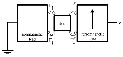
Here we study spin-resolved currents in a single-level quantum dot attached to a nonmagnetic lead (“left lead”) and to a ferromagnetic lead (“right lead”), Fig. 1. As we shall show, the magnetic asymmetry between the left and right terminals results in a rectification of the current polarization for a particular bias range for which the single electron channel is on-resonance, and the double-occupancy channel is off-resonance. More precisely, when the nonmagnetic lead operates as an emitter and the ferromagnetic lead as a collector, defined as the positive bias (), the current is unpolarized. In contrast, when the ferromagnetic lead is the emitter and the nonmagnetic lead is the collector (negative bias) a spin-polarized current arises. Importantly, this rectification occurs only in this particular bias range, as we shall demonstrate both analytically and numerically. This is attributed to an interplay between nonequilibrium spin accumulation and Coulomb interaction within the dot. For high enough bias voltages, the current polarization is essentially symmetric with respect to the bias, and no rectification is found.
In the main body of the text we employ the master-equation approach of Glazman and Matveevglaz-mat to describe the spin-dependent transport through the NM-QD-FM junction in the sequential tunneling regime (,glaz-mat where is a characteristic tunneling rate). An alternative description in terms of nonequilibrium Green functions is also presented in the appendix, that corroborates our results obtained via master equation.
II Model and Master Equation Approach
The NM-QD-FM system we study is schematically illustrated in Fig. 1. An external bias voltage drives the system away from equilibrium thus imposing a chemical potential imbalance between the left (L) and the right (R) leads: , where is the chemical potential of the lead and is the absolute value of the electron charge (). The system Hamiltonian is
| (1) | |||||
where is the free-electron energy with wave vector and spin in lead (), is the spin-degenerate dot level, is the on-site Coulomb repulsion and the operators () and () destroy (create) an electron with spin in the lead and in the dot, respectively. The matrix element gives the lead-dot coupling. We do not consider any spin-flip processes.
To calculate the current we use rate equations,wr01 ; glaz-mat which yield
| (2) | |||||
where we have assumed . The parameter corresponds to the rate of adding one electron to the dot coming from lead , and is the rate of moving one electron from the dot to lead . In addition, and give the rates of moving one electron with spin to and from the dot, respectively, when it is already occupied by one electron with opposite spin. Following Ref. [wr01, ] we define and () as the dot single and double average occupancies, respectively. The tunneling rates are
| (3) | |||||
| (4) | |||||
| (5) | |||||
| (6) |
where and . The rates and are related to the spin-resolved density of states of lead via and . Here we assume and . This reflects the fact that the density of states of the left lead is spin-degenerate while the right one is spin-split. Assuming a constant density of states and a constant tunneling parameter , we have . With this assumption the terms with in Eq. (2) cancel out,wr01 and one simply finds
| (7) |
To calculate the current via Eq. (7) we need to find fromwr01
| (8) | |||||
where
| (9) | |||||
| (10) | |||||
| (11) | |||||
| (12) |
When , Eq. (8) becomes
| (13) |
where the terms with cancel out.
Stationary regime. In this regime () Eq. (13) reduces to
| (14) |
which can be solved for each spin component, thus resulting in
| (15) |
where . Using Eq. (15) into Eq. (7) we obtain
| (16) |
From Eq. (16) we can readily evaluate the current polarization . Next (Sec. III) we provide some simple analytical results valid when double-occupancy is energetically forbidden. Numerical results are presented in Sec. IV.
III Regime of Singly occupied dot
As we shall see, the most interesting behavior takes place when the channel is completely within the conduction window and is far above the Fermi energy of the emitter. With this channel configuration we approximate , and , for and , for . Using this into the occupation and current equations, Eqs. (15) and (16), we find analytical expressions for the first plateau that appears in the current and its polarization for both positive and negative bias voltage. Equation (15) then becomes
| (17) |
where , for and , for . The current of the left lead then becomes
| (18) |
where and the sign corresponds to , while and the sign to . The right side current is simply given by for a spin-conserving stationary regime. Equation (18) gives the (bias-independent) current in the regime addressed here. For the particular case of spin-independent tunneling rates, i.e., and , we obtain
| (19) |
in accordance with results already known in the literature.glaz-mat ; at03yvn96
Using Eq. (18) into the definition , we obtain the current polarization plateau
| (20) |
where for and for . We model the tunneling rates by and , where is the spin polarization degree of the ferromagnetic right leadwr01 and the lead-dot coupling. Within this model Eq. (20) gives
| (23) |
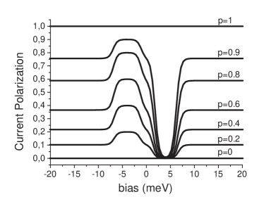
Thus, when only the level is within the conduction window, the current becomes unpolarized for positive bias, while spin-polarized for negative bias. Therefore the NM-QD-FM junction functions as a current-polarization diode.
IV RESULTS
IV.1 Parameters
We assume that the dot level depends on the bias voltage according to , where accounts for asymmetric voltage drops along the left and right tunnel barriers.wr01 ; wr03 can be controlled via gate voltages. For the numerics we take meV, , , eV, meV and eV.ak04 ; noteR2 In Secs. B, C and D we assume a symmetric potential drop across the system with . In Sec. E we briefly discuss the asymmetric case with .
IV.2 Current polarization
Figure 2 shows the current polarization as a function of the external bias . We observe that for positive bias the current polarization decreases for increasing bias, reaching zero around 4 meV. Conversely, for the negative biases we obtain a maximum polarization around meV, confirming the analytical result found in Sec. III, Eq. (23). The voltage range for this behavior scales with the parameter . For high enough bias voltages ( 7 meV) the polarization reaches the same nonzero plateaus for both positive and negative voltages. Both the suppression () and the enhancement () of the current polarization are due to the interplay of Coulomb interaction and spin accumulation in the quantum dot. Quite interestingly this interplay affects differently with the bias sign, namely, for direct bias it suppresses while for reverse bias it enhances .fms04these The suppression of for positive bias results in the zero polarization seen for all values except . In the half-metallic case (), there is only spin up current flowing in the system (, ), so the polarization becomes simply . On the other hand, for negative bias, the maximum polarization plateau changes as varies. In particular, attains a plateau equal to the polarization degree of the ferromagnetic lead, according to Eq. (23). To gain a more detailed understanding of the spin-diode effect we investigate next the spin accumulation and the spin-resolved curves as a function of the bias.
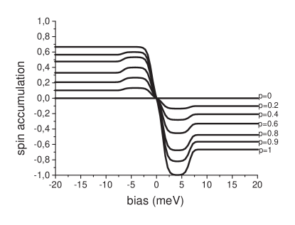
IV.3 Spin accumulation
Figure 3 shows the spin accumulation as a function of the bias voltage, for distinct polarization parameters . For all the values considered here we note that for positive bias and for negative bias. This spin-imbalance can be understood in terms of the tunneling rates between dot and leads. Due to the ferromagnetism of the right lead, the rates and become asymmetric. For example, for the rates are eV, eV and eV. For positive bias, becomes the ingoing tunneling rate for electrons with spin and the outgoing tunneling rate. Due to the inequality , the spin up electrons can tunnel out the dot faster than they come into it. On the other hand, since , the spin down electrons leave the dot slower than they come into it. So on average the spin down electrons spend more time in the dot than the spin up ones for , thus . A similar reasoning applies to the other values, except for for which there is no accumulation. For negative bias, and are the outgoing tunneling rates while and become the ingoing tunneling rates. As a consequence of this interchange, the spin accumulation inverts its sign . For small values the spin accumulation is essentially an odd function of the bias, Fig. 3.
When increases, though, the imbalance becomes stronger for positive bias. In particular for , reaches in the positive bias range corresponding to single occupancy (), and a constant plateau for all negative bias. This happens because no spin-down states are available in the right lead for , so a spin-down electron that enters the dot, coming from the left side (), cannot leave the dot to the right side. Hence a spin-up electron cannot hop into the dot when , so the accumulation becomes completely spin-down polarized for positive bias. For high enough bias voltages an additional electron with opposite spin can jump into the dot (for both positive and negative bias), thus resulting in a suppression (in modulus) of .
IV.4 Spin-resolved currents

In Figure 4 we show the spin resolved currents and as a function of the bias voltage for differing polarization parameters . We observe that for positive bias the spin up and spin down currents coincide in the plateaus indicated by arrows for any value. This results in the zero current-polarization seen in Fig. 2. In the second plateau, though, attains higher values compared to , which enhances . The strong suppression of in the first plateau () is attributed to the spin imbalance observed for the corresponding bias range (see Fig. 3). More specifically, since the dot is predominantly spin-down occupied for positive bias, the spin-up electrons tend to be more blocked than the spin-down ones, thus reducing further and interestingly locking it on top of . In contrast, for negative bias we have the population inversion . This gives a stronger suppression of as compared to , which enhances the difference between and , and consequently . When the channel reaches resonance ( meV) both the and plateaus attain values somewhat closer to each other, thus reducing the current polarization (see Fig. 2).
In particular for the is zero for any bias voltage since there are no spin-down states available in the right lead. The increases slightly (for positive bias) while the dot is becoming populated. When the population is high enough the Coulomb interaction plays a role and the spin up current goes down to zero.refbump This gives rise to a negative differential conductance at the beginning of the first plateau for [see Fig. 4 with ].jf05 For negative bias (and ) attains one plateau instead of two steps as for the other values. This is expected because the spin-down electrons do not participate in the transport in this case, so no Coulomb interaction effect arises. Note that for the system can operate as a mesoscopic current diode.iw06 ; mw05 ; rs04
IV.5 Effects of the bias-drop asymmetry
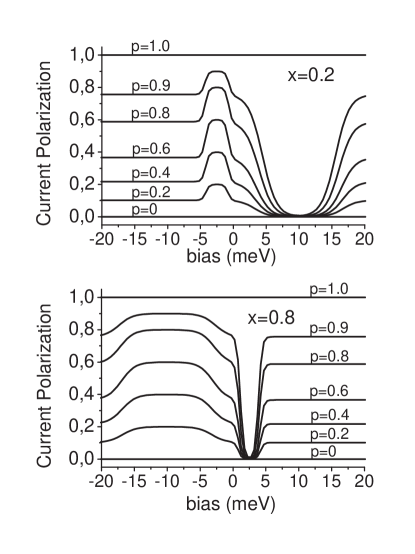
Here we consider the effects of an asymmetric bias drop, i.e., . As Fig. 5 shows, the asymmetry in the bias drop gives rise to quantitative, but not qualitative changes. For the current polarization goes to zero much slower with the bias than it does for . This is so because the resonance condition (), which is necessary to have [see Sec.(III)], happens for higher bias when decreases. For negative bias the resonance is reached faster (i.e., at lower biases as compared with the case) for decreasing . This, in turn, translates into a steeper enhancement of which then attains a plateau at [see Eq. (23)]. In addition, for the zero current-polarization plateau () enlarges while the maximum plateau () shrinks compared to the respective widths. For the resonance () takes place faster with the bias when compared to the and cases. This results in the steeper suppression of and the shrinkage of the zero current-polarization bias range. For negative biases the resonance condition for is more slowly attained with the bias as compared to the and cases. Consequently, the polarization reaches the plateau at for higher bias voltages (in modulus).
V Conclusion
We propose a NM-QD-FM system which operates as a diode for the current polarization. More specifically, when double-occupancy is forbidden in the system, i.e., the channel is far above the chemical potential of the emitter lead, the system carries an unpolarized current for positive bias and a spin-polarized current for negative bias. This effect is a result of the interplay between spin accumulation in the dot and the Coulomb interaction. Interestingly, for positive biases the spin-resolved currents and lock onto the same plateau for a particular bias range, thus resulting in .
VI Acknowledgments
The authors acknowledge G. Platero, K. Flensberg, T. Novotný, and J. P. Morten for helpful comments. FMS and JCE acknowledge the kind hospitality at the Centre for Advanced Study (Oslo) during the revision stage of this work. JCE acknowledges support from CNPq and FAPESP.
Appendix A Nonequilibrium Green functions
In the main text we have formulated the problem via master equation formalism. Here we show that Eqs. (17) and (18), from which our main result Eq. (23) directly follows, can be obtained via the Keldysh formalism. We start with the well known equation for the stationary currentMW92 ; apj94
where , and are the retarded, advanced and lesser Green functions, respectively. To calculate these we apply the equation of motion technique and use the Hartree-Fock approximation to factorize high-order correlation functions in the resulting chain of equations.hh96 The retarded Green function becomes
| (24) |
where is the non-interacting tunneling self-energy given in the wide band approximation by , and is the dot Green function without coupling to leads,
| (25) |
where is the dot occupation number, with . This occupation can be calculated self-consistently via
| (26) |
where the correlation function is given by the Keldysh equation
| (27) |
The advanced Green function is given by , while . In order to consider the same channel configuration adopted in Sec. III, we assume a large () so the retarded Green function becomes
| (28) |
and the lesser Green function reads
| (29) |
Substituting Eq. (29) into Eq. (26) we have
| (30) |
Now assuming that the dot level is completely on resonance within the conduction window between and for positive or negative biasapproximation we can integrate Eq. (30) in order to obtain
| (31) |
where for or for . Solving Eq. (31) for each spin component we find exactly Eq. (17).
To obtain Eq. (18) from the Green functions, we substitute Eqs. (28) and (29) into the current formula (A), which gives
| (32) |
Solving Eq. (32) with the same assumptions adopted previouslyapproximation we find
| (33) |
where and signs correspond to and , respectively. Eq. (33) can also be written as Eq. (18).
References
- (1) For an overview see e.g. Semiconductor Spintronics and Quantum Computation, eds. D. D. Awschalom, D. Loss, and N. Samarth, Springer, Berlin, 2002; I. Zutic, J. Fabian, and S. Das Sarma, Rev. Mod. Phys. 76, 323 (2004).
- (2) D. Loss and D. P. DiVincenzo, Phys. Rev. A 57, 120 (1998).
- (3) H.-A. Engel, P. Recher, and D. Loss, Sol. State Comm. 119, 229 (2001).
- (4) M. Wilczyński, R. Świrkowicz, W. Rudziński, J. Barnaś, and V. Dugaev, J. Magn. Magn. Mater. 290-291, 209 (2005).
- (5) R. Świrkowicz, M. Wilczyński, M. Wawrzyniak, and J. Barnaś, Phys. Rev. B 73, 193312 (2006).
- (6) J. Martinek, M. Sindel, L. Borda, J. Barnaś, R. Bulla, J. König, G. Schön, S. Maekawa, and J. von Delft, Phys. Rev. B 72, 121302(R) (2005).
- (7) Y. Utsumi, J. Martinek, G. Schön, H. Imamura, and S. Maekawa, Phys. Rev. B 71, 245116 (2005).
- (8) J. Martinek, Y. Utsumi, H. Imamura, J. Barnaś, S. Maekawa, J. König, and G. Schön, Phys. Rev. Lett. 91, 127203 (2003).
- (9) P. Zhang, Q.-K. Xue, Y. Wang, and X. C. Xie, Phys. Rev. Lett. 89, 286803 (2002).
- (10) F. Elste and C. Timm, Phys. Rev. B 73, 235305 (2006).
- (11) I. Weymann, J. Barnaś, J. König, J. Martinek, and G. Schön, Phys. Rev. B 72, 113301 (2005).
- (12) A. Cottet, W. Belzig, and C. Bruder, Phys. Rev. Lett. 92, 206801 (2004); A. Cottet and W. Belzig, Europhys. Lett. 66 (3), 405 (2004).
- (13) J. Barnaś and A. Fert, Phys. Rev. Lett. 80, 1058 (1998).
- (14) S. Takahashi and S. Maekawa, Phys. Rev. Lett. 80, 1758 (1998).
- (15) K. Walczak and G. Platero, CEJP 4(1), 30 (2006).
- (16) I. Weymann and J. Barnaś, Phys. Rev. B 73, 33409 (2006).
- (17) J. Varalda, A. J. A. de Oliveira, D. H. Mosca, J.-M. George, M. Eddrief, M. Marangolo, and V. H. Etgens, Phys. Rev. B 72, 81302(R) (2005).
- (18) I. Weymann, J. König, J. Martinek, J. Barnaś, and G. Schön, Phys. Rev. B 72, 115334 (2005).
- (19) F. M. Souza, J. C. Egues, and A. P. Jauho, Braz. J. Phys. 34, 565 (2004).
- (20) F. M. Souza, J. C. Egues, and A. P. Jauho, Proceedings of the 26th International Conference on the Physics of Semiconductors (ICPS 26), Edinburgh 2002, edited by J. H. Davies and A. R. Long. See cond-mat/0209263.
- (21) R. López and D. Sánchez, Phys. Rev. Lett. 90, 116602 (2003).
- (22) I. Weymann and J. Barnaś, Phys. Stat. Sol. (b) 236, 651 (2003).
- (23) W. Rudziński, J. Barnaś, and M. Jankowska, J. Mag. Mag. Mater. 261, 319 (2003).
- (24) W. Rudziński and J. Barnaś, Phys. Rev. B 64, 85318 (2001).
- (25) J. König and J. Martinek, Phys. Rev. Lett. 90, 166602 (2003).
- (26) M. Braun, J. König, and J. Martinek, Phys. Rev. B 70, 195345 (2004).
- (27) P. Recher, E. V. Sukhorukov, and D. Loss Phys. Rev. Lett. 85, 1962 (2000);
- (28) H.-A. Engel and D. Loss Phys. Rev. B 65, 195321 (2002);
- (29) E. Cota, R. Aguado, and G. Platero, Phys. Rev. Lett. 94, 107202 (2005).
- (30) A. Brataas, Y. V. Nazarov, J. Inoue, and G. E. W. Bauer, Phys. Rev. B 59, 93 (1999).
- (31) H. Imamura, S. Takahashi, and S. Maekawa, Phys. Rev. B 59, 6017 (1999).
- (32) J. Martinek, J. Barnaś, S. Maekawa, H. Schoeller, and G. Schön, Phys. Rev. B 66, 14402 (2002).
- (33) J. Wang, K. S. Chan, and D. Y. Xing, Phys. Rev. B 72, 115311 (2005).
- (34) W. Kuo and C. D. Chen, Phys. Rev. B 65, 104427 (2002).
- (35) I. Weymann and J. Barnaś, Phys. Rev. B 73, 205309 (2006).
- (36) R. Świrkowicz, J. Barnaś, M. Wilczyński, W. Rudziński, and V. K. Dugaev, J. Magn. Magn. Mater. 272-276, 1959 (2004).
- (37) H. Dalgleish and G. Kirczenow, Phys. Rev. B 73, 235436 (2006).
- (38) A. A. Shokri, M. Mardaani, and K. Esfarjani, Physica E 27, 325 (2005)
- (39) L. I. Glazman and K. A. Matveev, JEPT Lett.48, 445 (1988).
- (40) Y. V. Nazarov and J. J. R. Struben, Phys. Rev. B 53, 15466 (1996); A. Thielmann, M. H. Hettler, J. König, and G. Schön, Phys. Rev. B 68, 115105 (2003).
- (41) Typical values of and can be found in, for example, A. Kogan et al., Phys. Rev. Lett. 93, 166602 (2004); F. Simmel et al. Phys. Rev. Lett. 83, 804 (1999); D. Goldhaber-Gordon et al., Nature 391, 156 (1998).
- (42) In the context of nonequilibrium Green function (see Appendix) we note that by increasing the coupling parameter , the width of the dot level increases as well, thus resulting in more smooth curves in Figs. 2-5.
- (43) For a system with two ferromagnetic leads coupled to a quantum dot (FM-QD-FM), it is possible to have an enhancement of for negative biases and a suppression of for positive biases when the lead magnetizations are aligned antiparallel. However, the polarization does not vanish for any particular bias range and consequently no rectification effect is observed - F. M. Souza, PhD thesis, University of São Paulo, Brazil (2004).
- (44) A similar bump in the total current () was also seen in B. R. Bulka, Phys. Rev. B 62, 1186 (2000), and also in [mw05, ], [wr03, ] and [wr01, ].
- (45) A negative differential resistance was also seen in J. Fransson, Phys. Rev. B 72, 75314 (2005).
- (46) Y. Meir and N. S. Wingreen, Phys. Rev. Lett. 68, 2512 (1992).
- (47) A. P. Jauho, N. S. Wingreen, and Y. Meir, Phys. Rev. B 50, 5528 (1994).
- (48) H. Haug and A. P. Jauho, Quantum Kinetics in Transport and Optics of Semiconductors, Springer Solid-State Sciences 123 (1996).
- (49) More precisely we assume that for and for . In addition we approximate and for and and for .