Pulse and hold strategy for switching current measurements
Abstract
We investigate by theory and experiment, the Josephson junction switching current detector in an environment with frequency dependent damping. Analysis of the circuit’s phase space show that a favorable topology for switching can be obtained with overdamped dynamics at high frequencies. A pulse-and-hold method is described, where a fast switch pulse brings the circuit close to an unstable point in the phase space when biased at the hold level. Experiments are performed on Cooper pair transistors and Quantronium circuits, which are overdamped at high frequencies with an on-chip RC shunt. For 20 µs switch pulses the switching process is well described by thermal equilibrium escape, based on a generalization of Kramers formula to the case of frequency dependent damping. A capacitor bias method is used to create very rapid, 25 ns switch pulses, where it is observed that the switching process is not governed by thermal equilibrium noise.
I Introduction
A classical non-linear dynamical system, when driven to a point of instability, will undergo a bifurcation, where the system evolves toward distinctly different final states. At bifurcation the system becomes very sensitive and the smallest fluctuation can determine the evolution of a massive system with huge potential energy. This property of infinite sensitivity at the point of instability can be used to amplify very weak signals, and has recently been the focus of investigation in the design of quantum detectors to readout the state of quantum bits (qubits) built from Josephson junction (JJ) circuits. Here we examine in experiment and theory a pulse and hold strategy for rapid switching of a JJ circuit which is quickly brought near a point of instability, pointing out several important properties for an ideal detector. We focus on switching in a circuit with overdamped phase dynamics at high frequencies, and underdamped at low frequencies. This HF-overdamped case is relevant to experiments on small capacitance JJs biased with typical measurement leads.
Classical JJs have strongly non-linear electrodynamics and they have served as a model system in non-linear physics for the last 40 years. More recently it has been shown that JJ circuits with small capacitance can also exhibit quantum dynamics when properly measured at low enough temperatures. Experimental demonstration of the macroscopic quantum dynamics in these circuits has relied on efficient quantum measurement strategies, characterized by high single shot sensitivity with rapid reset time and low back action. Some of these measurement or detection methods are based on the switching of a JJ circuit from the zero voltage state to a finite voltage state. Vion et al. (2002); Chiorescu et al. (2003); Martinis et al. (2002); Plourde et al. (2005) Other detection methods are based on a dispersive technique, where a high frequency signal probes the phase dynamics of a qubit.Il’ichev et al. (2003); Born et al. (2004); Siddiqi et al. (2004); Grajcar et al. (2004); Wallraff et al. (2004); Roschier et al. (2005); Duty et al. (2005); Lupaşcu et al. (2006) These dispersive methods have achieved the desired sensitivity at considerably higher speeds than the static switching methods, allowing individual quantum measurements to be made with much higher duty cycle. In particular, the dispersive methods have shown that it is possible to continuously monitor the qubit.Wallraff et al. (2005) However, for both static switching and dispersive methods, the sensitivity of the technique is improved by exploiting the non-linear properties of the readout circuit in a pulse and hold measurement strategy. This improved sensitivity of the pulse and hold method is not surprising, because when properly designed, the pulse and hold technique will exploit the infinite sensitivity of a non-linear system at the point of instability.
The general idea of exploiting the infinite sensitivity at an instable point is a recurrent theme in applications of non-linear dynamics. The basic idea has been used since the early days of microwave engineering in the well-known parametric amplifierLouisell (1960) which has infinite gain at the point of dynamical instability. The unstable point can be conveniently represented as a saddle point for the phase space trajectories of the non-linear dynamical system. In the pulse and hold measurement method an initial fast pulse is used to quickly bring the system to the saddle point for a particular hold bias level. The hold level is chosen so that the phase space topology favors a rapid separation in to the two basins of attraction in the phase space. The initial pulse should be not so fast that it will cause excessive back action on the qubit, but not so slow that it’s duration exceeds the relaxation time of the qubit. The length of the hold pulse is that which is required to achieve a signal to noise ratio necessary for unambiguous determination of the resulting basin of attraction. In practice this length is set by the filters and amplifiers in the second stage of the quantum measurement system.
In this paper we discuss pulse and hold detection in the context of switching from the zero voltage state to the finite voltage state of a JJ. We give an overview of such switching in JJs, focusing on the HF-overdamped case. Switching detectors with overdamped high frequency phase dynamics are different from all other qubit measurement strategies implemented thus far, where underdamped phase dynamics has been used. However, the HF-overdamped case is quite relevant to a large number of experiments which measure switching in low capacitance JJs with small critical currents.Joyez et al. (1999); Ågren et al. (2002); Cottet et al. (2002); Männik and Lukens (2004) We show that by making the damping at high frequencies large enough, a favorable phase space topology for switching can be achieved.Sjöstrand et al. (2006) In this overdamped situation the external phase can be treated classically and contributions of macroscopic quantum tunneling (MQT) to the switching probability can be neglected, in contrast to the underdamped case.Ithier et al. (2005) Experimental results are shown where on-chip RC damping circuits are used to create an HF-overdamped environment. We observe that for longer pulses of duration 20 µs, the switching process is initiated by thermal fluctuations in the overdamped system and thermal equilibrium is achieved at the base temperature of the cryostat (25 mK). For short pulses of duration ns, the switching is unaffected by thermal fluctuations up to a temperature of 500 mK, and the width of the switching distribution at low temperatures is rather determined by random variations in the repeated switch pulse. Although the detector apparently had the speed and sensitivity required for making a quantum measurement, we were unfortunately unable to demonstrate quantum dynamics of the qubit due to problems with fluctuating background charges.
II Phase Space Portraits
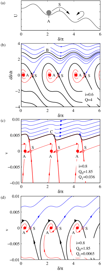
The non-linear dynamics of a DC-driven JJ can be pictorially represented in a phase space portrait. We begin by examining the phase space portraits of the resistive and capacitively shunted junction (RCSJ), which is the simplest model from which we can gain intuitive understanding of the non-linear dynamics. The RCSJ model consists of an ideal Josephson element of critical current biased at the current level , which is shunted by the parallel plate capacitance of the tunnel junction, and a resistor , which models the damping at all frequencies (see fig. 1(a)). The circuit parameters define the two quantities called the plasma frequency, and the quality factor . The dynamics is classified as overdamped or underdamped for or , respectively. Here is the reduced flux quantum.

The circuit dynamics can be visualized by the motion of a particle of mass in a tilted washboard potential subjected to the damping force , where the particle position corresponds to the phase difference across the junction and the tilt is the applied current normalized by the critical current, (see fig 2(a)). Below the critical tilt the fictitious particle will stay in a local minimum of the washboard potential (marked A in fig 2(a)) corresponding to the superconducting state where . Increasing the tilt of the potential to , where local minima no longer exist, the particle will start to accelerate to a finite velocity determined by the damping. If the tilt is then decreased below , the particle for an underdamped JJ () will keep on moving due to inertia. Further decreasing the tilt below the level , where loss per cycle from damping exceeds gain due to inertia, the particle will be retrapped in a local minimum. In terms of the current-voltage characteristic, this corresponds to hysteresis, or a coexistence of two stable states, and for a bias fixed in the region . For the overdamped RCSJ model the particle will always be trapped in a local minimum for and freely evolving down the potential for and there is no coexistence of two stable states.
A phase space portraitKautz (1988); Hänggi et al. (1990); Sjöstrand et al. (2006) of the RCSJ model is shown in fig. 2(b). This portrait shows trajectories that the particle would follow in the space of coordinate () versus velocity () for a few chosen initial conditions. The topology of the phase space portrait is characterized by several distinct features. Fix point attractors marked “A” in fig. 2 correspond to the particle resting in a local minimum of the washboard potential, and the saddle points marked “S” corresponds to the particle resting in an unstable state at the top of the potential barrier (compare with fig. 2(a)). Two trajectories surrounding A and ending at S are the unstable trajectories which define the boundary of a basin of attraction: All initial conditions within this boundary will follow a trajectory leading to A. We call this the 0-basin of attraction. The thick line B is a stable limiting cycle, corresponding to a free-running state of the phase , where the circuit is undergoing Josephson oscillations with frequency . All trajectories leading to the limiting cycle B start in the 1-basin of attraction, which is the region outside the 0-basins. The existence of two basins of attraction in the phase space topology, and in particular the clear separation of all 0-basins by the 1-basin, make the underdamped RCSJ circuit () appropriate for a switching current detector, as we discuss below. For the overdamped RCSJ circuit () attractors A and B do not coexist for any fixed bias condition, and it therefore can not be used for a switching current detector. However, the RCSJ model is not always the most realistic model for the dynamics of JJ circuits, as the damping in real experiments is usually frequency dependent, and in the case of small capacitance JJs, this frequency dependence can very much change the character of the damping.
At high frequencies of the order of the plasma frequency of the junction (20-100 GHz for Al/AlOx/Al tunnel junctions) losses are typically due to radiation phenomena, where the leads to the junction act as a wave guide for the microwave radiation. If we model the leads as a transmission line, the high frequency impedance would correspond to a damping resistance of the order of free space impedance . With the small capacitance of a typical JJ as used in present experiments, this damping inevitably leads to overdamped dynamics . It should be noted that for small capacitance JJs, underdamped phase dynamics is hard to achieve in practice as high impedance all the way up to the plasma frequency is desired, and this requires an engineering effort where the high impedance leads need to be constructed very close to the junction. Corlevi et al. (2006) However, at lower frequencies (typically below MHz) the junction will see an impedance corresponding to the bias resistor at the top of the cryostat, which can be chosen large enough to give . The simplest circuit which captures the frequency dependence described above, is a JJ shunted by a series combination of a resistor and a capacitor in parallel with the resistor as shown in fig. 1(b). At high frequencies where is essentially a short, the circuit is described by the high-frequency quality factor , where is the parallel combination of and . At low frequencies where effectively blocks, the quality factor reads . This model has been studied previously by several authors.Ono et al. (1987); Kautz and Martinis (1990); Vion et al. (1996); Joyez et al. (1999); Sjöstrand et al. (2006) Casting such a circuit in a more mathematical language, it can be described by the coupled differential equations Kautz and Martinis (1990); Sjöstrand et al. (2006)
| (1) | |||||
where is the reduced voltage across and reflects the value of the transition frequency, being , between high- and low-impedance regimes.
Phase space portraits for such a circuit are shown in figs. 2(c) and (d). Here the y-axis shows the voltage which is directly related to . The topology of this phase portrait is also characterized by the coexistence of fix-points A and the limiting cycle B (not shown). However, for the parameters of fig. 2(c) (, and . ), the 0-basins and the 1-basin are now separated by an unstable limiting cycle C which does not intersect a saddle point. An initial condition which is infinitesimally below or above C will eventually end up either in an attractor A, or on B respectively. In fig. 2(c) we also see that the boundaries of the 0-basins are directly touching one another as a consequence of the existence of C. Thus, it is possible to have a trajectory from one 0-basin to another 0-basin, without crossing the 1- basin.
This same HF-overdamped model can however produce a new topology by simply lowering the high-frequency quality factor . As we increase the high frequency damping, the unstable limiting cycle C slowly approaches the saddle points S. For a critical value of , C and S will touch and the phase-portrait suddenly changes its topology. Fig. 2(d) shows the phase space portrait for , and where we can see that C disappears and adjacent 0-state basins are again separated by the 1-basin – a topology of the same form as the underdamped RCSJ model.
III The Switching Current Detector
The transition from the 0-basin to the 1-basin, called switching, can be used as a very sensitive detector. The idea here is to choose a ”hold” bias level and circuit parameters where the phase space portrait has a favorable topology such as that shown in figs. 2(b) and (d). A rapid ”switch pulse” is applied to the circuit bringing the system from A to a point as close as possible to the unstable point S. Balanced at this unstable point, the circuit will be very sensitive to any external noise, or to the state of a qubit coupled to the circuit. The qubit state at the end of the switch pulse can be thought of as determining the initial condition, placing the fictitious phase particle on either side of the basin boundary, from which the particle will evolve to the respective attractor. The speed and accuracy of the measurement will depend on how rapidly the particle evolves away from the unstable point S, far enough in to the 0-basin or 1-basin such that external noise can not drive the system to the other basin. From this discussion it is clear that a phase space portrait with the topology shown in fig. 2(c) is not favorable for a switching current detector. Here the switching corresponds to crossing the unstable cycle C. Initial conditions which are infinitesimally close to C will remain close to C over many cycles of the phase, and thus a small amount of noise can kick the system back and forth between the 0-basins and the 1-basin, leading to a longer measurement time and increased number of errors.
The measurement time is that time which is required for the actual switching process to occur and must be shorter than the relaxation time of the qubit. In the ideal case the measurement time would be the same as the duration of the switch pulse. A much longer time may be required to actually determine which basin the system has chosen. This longer detection time is the duration of the hold level needed to reach a signal to noise ratio larger than 1, which is in practice determine by the bandwidth of the low-noise amplifier and filters in the second stage of the circuit. In our experiments described in the following sections, we used a low noise amplifier mounted at the top of the cryostat which has a very limited bandwidth and high input impedance. While this amplifier has very low back action on the qubit circuit (very low current noise), it’s low bandwidth increases the detection time such that individual measurements can be acquired only at kHz repetition rate. Since many measurements () are required to get good statistics when measuring probabilities, the acquisition time window is some 0.5 seconds and the low frequency noise (drift or noise) in the biasing circuit will thus play a role in the detector accuracy.
IV Fluctuations
The measurement time of a switching detector will depend on fluctuations or noise in the circuit. The phase space portraits display the dissipative trajectories of a dynamical system, but they do not contain any information about the fluctuations which necessarily accompany dissipation. For a switching current detector, we desire that these fluctuations be as small as possible, and therefore the dissipative elements should be kept at as low a temperature as possible. Analyzing the switching current detector circuit with a thermal equilibrium model, we can calculate the rate of escape from the attractor A. This equilibrium escape rate however only sets an upper limit on the measurement time. When we apply the switch pulse, the goal is to bring the circuit out of equilibrium, and we desire that the sensitivity at the unstable point be large enough so that the measurement is made before equilibrium is achieved (i.e. before thermal fluctuations drive the switching process).
Equilibrium fluctuations can cause a JJ circuit to jump out of it’s basin of attraction in a process know as thermal escape. The random force which gives rise to the escape trajectory will most likely take the system through the saddle point S, because such a trajectory would require a minimum of energy from the noise source. Kautz (1988) For the topology of phase space portraits shown in figs. 2(b) and (d), thermal escape will result in a switching from a 0-basin to the 1-basin, with negligible probability of a ”retrapping” event bringing the system back from the 1-basin to a 0-basin. However, for the topology of fig. 2(c), thermal escape through the saddle point leads to another 0-basin, and thus the particle is immediately retrapped in the next minimum of the washboard potential. This process of successive escape and retrapping is know as phase diffusion, and it’s signature is a non-zero DC voltage across the JJ circuit when biased below the critical current, .
Phase diffusion can occur in the overdamped RCSJ model, or in the HF-overdamped model when parameters result in a phase space topology of fig. 2(c). In the latter case, a switching process can be identified which corresponds to the escape from a phase diffusive state to the free running state, or to crossing the unstable limiting cycle C in fig. 2(c) which marks the boundary between the phase diffusive region and the 1-basin. This basin boundary C is formed by the convergence of many trajectories leading to different S, and the escape process of crossing this boundary is fundamentally different than escape from a 0-basin to the 1-basin. Numerical simulations Sjöstrand et al. (2005, 2006); Sjöstrand (2006) of switching in JJs with such a phase space topology show that escape over the unstable boundary C is characterized by late switching events, which arise because even a small amount of noise near this boundary can kick the system back and forth between the 1-basin and the many 0-basins for a long time before there is an actual escape leading to the limiting cycle B.
The rate of thermal escape from a 0-basin can be calculated using Kramers’ formula Kramers (1940); Hänggi et al. (1990); Mel’nikov (1991)
| (2) |
with being the depth of the potential well from A to S, Boltzmann’s constant and the temperature. The prefactor is called the attempt frequency, where is a factor which depends on the damping. Analytical results for were found by Kramers in the two limiting cases of underdamped () and overdamped () dynamics. For the application of Kramers’ escape theory we require that , i.e. thermal escape is rare, so that each escape event is from a thermal equilibrium situation. The fluctuations in thermal equilibrium are completely uncorrelated in time, which is to say that the strength of the fluctuations are frequency independent (white noise). Furthermore, the Kramers formula assumes absorbing boundary conditions, where the escape process which leads to a change of the basin of attraction has zero probability of return. These conditions restrict the direct application of Kramers formula in describing switching in JJ circuitsBüttiker et al. (1983) to the case of the underdamped RCSJ model such as that depicted in fig. 2(b). In principle one could apply Kramers formula to the overdamped RCSJ model, where the escape is from one well to the next well (switching between adjacent attractors A), but experiments thus far are unable to measure a single jump of the phase, as this corresponds to an extremely small change in circuit energy.
Thermal induced switching of small capacitance Josephson junctions which experience frequency dependent damping as modeled by the circuit of Fig. 1(b), was analyzed in experiment and theory by the Quantronics group Vion et al. (1996); Joyez et al. (1999) who generalized Kramers result. The theoretical analysis was subject to the constraint that the dynamics of the voltage across the shunt capacitor is underdamped (i.e. the quality factor where is the parallel resistance of and ) so that the dynamics of is subject to the fast-time average effects of the fluctuating phase . Separating timescales in this way, the switching of could then be regarded as an escape out of a meta-potential, , formed by the averaged fluctuating force in the tilted washboard potential . Assuming non-absorbing boundary conditions, this ”escape over a dissipation barrier” can be written as a generalization of Kramers’ formula
| (3) |
Here is the position-dependent diffusion constant, and , where and stand for the bottom and the top of the effective barrier, respectively. Detailed expressions can be found in refs.Götz (1997); Joyez et al. (1999)
In section VI, we use these escape rate formulas to analyze pulse and hold switching measurements. We demonstrate that long switching pulses lead to thermal equilibrium switching, whereas short pulses switch the circuit in a way that is independent of temperature at low temperatures, with the switching distribution determined by noise in the switch pulse rather than noise from the cooled damping circuit.
V Experiments
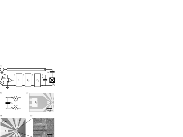
Experiments investigating junction current-voltage characteristics (IVC) as well as pulsed switching behavior were carried out in a dilution refrigerator with mK base temperature. A block diagram of the measurement setup is shown in fig. 3(a). A low noise instrumentation amplifier (Burr-Brown INA110, noise temperature K at kHz) is measuring the voltage across the sample while the sample is biased by a room temperature voltage source either via the bias capacitor , or in series with a bias resistor . The capacitor bias method was used for experiments with fast current pulses of duration ns, while the conventional resistor bias method was used for long pulse experiments with µs, as well as for IVC measurements.
Three different samples are discussed in this paper which differ primarily in the range of the measured switching current (3 nA to 120 nA), and in the type of circuit used for the damping of the phase dynamics. These different damping circuits are labeled in the order in which they were implemented, and are represented in fig. 3(a) as the blocks . These environments can be modeled as RC filters with different cut-off frequencies, as schematically be represented in fig. 3(b).
| CPT | Shunt JJ | ||||||||||||
| Sample | Type | ||||||||||||
| I | CPT | 32.9 | 58.5 | 3 | - | - | - | 60 | 1 | - | - | - | - |
| II | CPT | 29 | 51.6 | 4.2 | - | - | - | 60 | 1 | 7.2 | 0.24 | - | - |
| III | Quantronium | 2.2 | 21 | 12 | 30.3 | 158 | 120 | 1000 | 3 | 7.2 | 0.24 | 600 | 1.4 |
The key parameters for each sample are given in Table 1. Sample I consisted of a Cooper pair transistor (CPT) embedded in an environment defined solely by the twisted pair leads of the cryostat which is modeled as . Sample II was a CPT fabricated in parallel with Sample I, having nearly identical parameters, differing only in that sample II was embedded in a micro-fabricated on-chip HF-damping circuit . Sample III is a Quantronium Vion et al. (2002) embedded in the same HF-damping used with sample II, but with an additional micro-fabricated on-chip low-pass filter . The on-chip RC-environments and used for samples II and III and the bias capacitor were fabricated with a two-step optical lithography process. The capacitors were actually two capacitors in series, formed by a plasma-oxidized Al ground plane covered with a Au top plate. The top plates are connected to the rest of the circuit via resistors which are formed from the same Au film as the top plate, having a typical sheet resistance of . The capacitors of could be measured quite accurately, from which we obtain a specific capacitance of 13.6 fF/µm2 that is used to determine all on-chip capacitors. Figure 3(c) shows the essential parts of the chip and the components defining the high-frequency environment. The bright rectangular area on the left side is the top plate of the capacitor, and the thin leads leading to the right are the resistors of filter . Figure 3(d) shows in detail the biasing capacitor The bright trapezoidal area on the left is the top plate of the capacitor and the areas surrounded by dashed lines are damping resistors . Figure 3(e) is an electron microscope picture showing the tunnel junctions, which were fabricated in a third layer of electron beam lithography, with the standard two-angle evaporation through a shadow mask. Figure 3(e) shows the quantronium circuit of sample III.
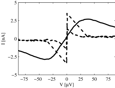
The effect of the on-chip HF damping from on the phase dynamics as can be seen in fig. 4 where the IVC of samples I (solid line) and sample II (dashed line) are shown. These two CPT samples differ essentially by the presence of in sample II. We see that the typical phase diffusion shape of the IVC Steinbach et al. (2001) of sample I is absent in sample II which shows a sharp supercurrent and hysteretic switching. The presence of the on-chip environment in sample II effectively reduces phase diffusion as can be explained by a phase-space topology as shown in figure 2(d). However, the very low value of is a direct indication of excessive noise in the circuit. Therefore the on-chip low-pass filter was implemented in sample III, improving the switching current to a value of of the critical current. In the remainder of this paper we concentrate on investigating the switching behavior of sample III.
The ability to suppress phase diffusion opens up the possibility to study fast switching with HF-overdamped phase dynamics for the first time. We used the pulse and hold method to measure switching probabilities of sample III as a function of the amplitude of the switch pulse for two cases: A long pulse of 20 µs where the switching was found to be controlled by equilibrium thermal escape, and a short pulse of 25ns, where the switching is clearly a non-equilibrium process.
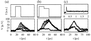
The long pulses were formed by applying a square voltage pulse through the bias resistor. The response to a simple square pulse is shown in fig. 5(a), where the applied voltage pulse is shown, and several scope traces of the measured voltage over the CPT are overlayed. Here we see that the switching causes an increase in the voltage over the sample which can occur at any time during the applied pulse. In order to do statistics we want to unambiguously count all switching events. Late switching events are difficult to distinguish from non-switching events as the voltage does not have time to rise above the noise level. We can add a trailing hold level as shown in fig. 5(b). This hold level and duration must be chosen so that there is zero probability of switching on the hold part of the pulse. The response to such a pulse shows that it is now easy to distinguish switch from non-switch events. In this case the hold level is used simply to quantize the output, and the switching which occurs during the initial switch pulse is found to be a thermal equilibrium escape process as discussed below.
The fast pulses were formed with a new technique where a voltage waveform consisting of a sharp step followed by linear voltage rise is programmed in to an arbitrary waveform generator. The slope on the sharp step is typically 6–7 times larger than the linear rise during the hold, . The voltage waveform is propagated to the chip through a coax cable having negligible dispersion for the sharp 25 ns voltage step used. An on-chip bias capacitor will differentiate the voltage waveform to give a sharp current pulse followed by a hold level, , which is shown in fig. 5(c). From the measured step amplitude needed to switch the junction and the value of pF, we calculate a pulse amplitude of 360 nA through . Due to the symmetry of the filter stages to , only half of this 25 ns pulse current flows through the junction, with the other half flowing through the filter to ground. Thus the peak current through the junction during the 25 ns pulse nA, which is larger than . Exceeding for this very short time is not unreasonable, bearing in mind that the circuit is heavily overdamped at high frequencies, and a strong kick will be needed to overcome damping and bring the phase particle close to the saddle point.
The hold level for these fast pulses is µs,very much longer than the switch pulse, and its duration is set by the time needed for the response voltage to rise above the noise level. The rate of this voltage rise depends on the hold current level because after the switch we are essentially charging up the second stage filter and leads, and , with the hold current, nA. For the low level of hold current used in these experiments, we can follow the voltage rise at the junction with the 100 kHz bandwidth low noise amplifier at the top of the cryostat. Typically we turn off the hold current and reset the detector when the sample voltage is 30 µV, so that the junction voltage is always well below the gap voltage µV, and therefore quasi-particle dissipation during the hold can be neglected.
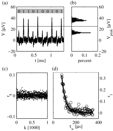
Pulsed switching measurements were performed were a sequence of to identical pulse-hold-reset cycles was applied to the sample while recording the voltage response of the sample. A threshold level was used to distinguish switching events (1) from non-switching events (0) as depicted in fig. 6(a). The maximum response voltage achieved during each cycle is found and a histogram of these values is plotted as seen in fig. 6(b). The hold level and duration are adjusted so as to achieve a bimodal distribution in the histogram, with zero events near the threshold level, meaning that there is zero ambiguity in determining a switch event from a non-switch event. We further check that the hold level itself, without the leading switch pulse, gives no switches of the sample. The sequence of switching events is stored as a binary sequence in temporal order. From this sequence we can calculate the switching probability,
| (4) |
and the auto-correlation coefficients,
| (5) |
where is the ”lag” between pulses. The auto-correlation is a particularly important check for statistical independence of each switching event. A plot of for is shown in figure 6(c) and the randomness and low level of indicates that all switching events are not influenced by any external periodic signal. When the circuit is not working properly, pick up of spurious signals up to the repetition frequency of the measurement, clearly shows up as a periodic modulation in the auto-correlation . Of particular importance is the correlation coefficient for lag one which tells how neighboring switching events influence one another. Fig. 6(d) shows as a function of the wait time between the end of the hold level and the start of the next switch pulse. For large values of , fluctuates around 0 not exceeding 0.05, which shows that any influence of a switching or non-switching event on the following measurement, is statistically insignificant. As is decreased however, a positive correlation is observed, with increasing exponentially with shorter . Positive correlation indicates that a switching event (a ”1”) is more likely to be followed by another switching event. Fig. 6(d) shows a fit to correlation to the function
| (6) |
We can extrapolate the fit to the time µs where the auto-correlation becomes , meaning that once the circuit switches it will always stay in the 1-state. In our experience, increasing the capacitance of filter causes to increase, from which we infer that the increase in the correlation for short is resulting from errors where the detector is not properly reset because it does not have time to discharge the environment capacitance before a new pulse is applied. For the experiment shown in figure 6 the time constant of the environment was estimated to be 3 µs. These observations indicate that it is necessary to bring the junction voltage very close to zero before the retrapping will occur, and the detector will reset. For good statistics many pulses are required and a short duty cycle is desirable in order to avoid effects from low frequency noise as discussed section III. By studying the correlation coefficient in this way, we can choose an optimal duty cycle.
VI Analysis
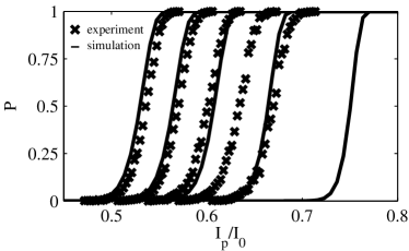
The switching probabilities were thus measured and the dependence on the amplitude of the switch pulse, was studied as as a function of temperature. Each measurement of began with a pulse sequences having pulse amplitude resulting in a switching probability , and the pulse amplitude was successively increased until . The measurement produces an ”S-curve” as shown in figure 7, where the experimental data for the long pulse duration µs is shown with crosses. The S-curves were taken at temperatures 100, 200, 300, 400 and 500 mK (right to left) respectively.
We compare the measured data to theoretical predictions based on thermal escape as discussed in section IV. The filter causes a rounding of the applied square voltage pulse, which is accounted for by calculating the escape probability for a time dependent current Götz (1997),
| (7) |
where the escape rate can be found using either eqns. 2 or 3. The simulated S-curves using eqn. 3 are plotted in figure 7 as solid lines for the temperatures corresponding to the measured data. Sample parameters used for this calculation are the measured bias (including filter) resistance , the measured high frequency damping resistor, , the high frequency damping capacitance nF, the junction capacitance fF, and the calculated critical current nA. The critical current nA is not the bare critical current nA since the quantronium was biased at a magnetic field such that a persistent current of nA was flowing in the loop. These parameters are all independently determined, and not adjusted to improve the fit. However, the capacitance of filter was uncertain, having a nominal value of 10nF, and unknown temperature dependence below K. Cooling the same capacitance to K, we observed a decrease of by around . This capacitor determines the rounding of the square voltage pulse, and thus the time dependence of the current applied to the junction. We found that it was necessary to assume nF in order for the simulations to agree with experiment. This low value of at low temperatures is not unreasonable, as circuit simulations with the nominal value of 10 nF showed that the initial pulse would not exceed the hold level, which clearly is not possible because excellent latching of the circuit was observed.
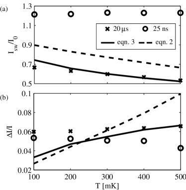
From the experimental and simulated S-curves, we define the switching current of the sample as the pulse amplitude that gives 50 % switching and the resolution is defined from the S-curve by . A comparison of experimental and theoretical vs. and vs. is shown in fig. 8. We see that the experimental data for the long pulses (points marked by an X) are in reasonably good agreement with the simulated values when the theory of switching in an environment with frequency dependent damping is used (escape from a meta-potential, equation 3) which is plotted as a solid line in fig. 8(a). We note that for the 20 µs pulses, escape occurs at bias currents , where the phase space has a topology as shown in figure 2(d). Hence we can neglect phase diffusion and escape is from a saddle point, so that the non-absorbing boundary condition assumed in the theory is valid. For comparison, we use the overdamped Kramers formula (equation 2) to simulate the S-curve and calculate and , which is shown by the dashed line in fig. 8. Here the prefactor is given in ref.Kautz and Martinis (1990) and we have used the high frequency quality factor as determined by the resistor only. We see that the Kramers formula overestimates by some 25% (fig. 8(a)) and is worse than the simulation based on eqn. 3, in reproducing the temperature dependence of (fig. 8(b)). In fact, the experimental data for the µs pulses only shows a weak increase in over the temperature range studied, whereas both theoretical curves predict a slight increase in . Thus an equilibrium thermal escape model explains the data for long, 20 µs pulses reasonably well and the data is better explained by the theory of escape with frequency dependent damping, than by the simpler theory embodied in the overdamped Kramers formula. However the correspondence with the former theory is not perfect. We may explain these deviations as being due to the fact that the quality factor (see section IV) does not really satisfy the condition for validity of the theory, .
Experimental data for the short pulses of duration ns generated by the capacitive bias method is plotted in fig. 8 as circles. Here we see that the value of is constant in the temperature range studied, indicating that escape is not from a thermal equilibrium state. For the ideal phase space topology, as shown in figure 2(d), the initial pulse would bring the phase particle arbitrarily close to the saddle point S for the hold bias level. If the separation in to the basins of attraction occurs before thermal equilibrium can be established, we would not expect temperature dependence of . In this case, the width of the switching distribution will be determined not by thermal fluctuations, but by other sources of noise, such as random variation in the height of the switch pulse. These variations are significant because the 1/f noise from the waveform generator must be taken in to account when generating the train of pulses over the time window of the measurement which was about 0.5 sec. In our experiments however, we may not have achieved a constant hold level since the voltage ramp from the waveform generator is not perfectly smooth. Knowing the bias capacitor we can calculate an average hold level of , somewhat lower than the critical value of necessary to achieve the phase space topology of figure 2(d). Nevertheless, we observe excellent latching of the circuit for these 25 ns switch pulses. We conclude that the observed temperature independence of , and the fact that exceeds by 20% is consistent with a very rapid switching of the junction.
We can rule out excessive thermal noise as a reason for the temperature independent value of for the short pulses. By measuring the gate voltage dependence of as a function of the temperature, a clear transition from to periodicity was observed in the temperature range 250 mK to 300 mK. For the size of the superconducting island used in this experiment, we can estimate a crossover temperature mK, above which the free energy difference between even and odd parity goes to zero.Tuominen et al. (1992) Hence, we know that the sample is in equilibrium with the thermometer below , and therefore heating effects that might occur in the short pulse experiments, can not explain the fact that the observed is independent of temperature.
Thus we have achieved a very rapid, 25 ns measurement time of the switching current, which should be sufficient for measurement of the quantum state of a quantronium circuit. For qubit readout, not only the measurement time is important, but also the resolution of the detector. For the 25 ns pulse, we obtained the resolution of , or nA. This implies that single shot readout is possible for a Quantronium with parameters K and where the switching current of the two qubit states at the optimal readout point differ by 9.6 nA. Numerous experiments were made with microwave pulses and continuous microwave radiation to try and find the qubit resonance. However, due in part to uncertainty in the qubit circuit parameters (level separation) and in part to jumps in background charge, no qubit resonance was detected in these experiments.
VII Conclusion
Fast and sensitive measurement of the switching current can be achieved with a pulse-and-hold measurement method, where an initial switch pulse brings the JJ circuit close to an unstable point in the phase space of the circuit biased at the hold level. This technique exploits the infinite sensitivity of a non-linear dynamical system at a point of bifurcation, a common theme in many successful JJ qubit detectors. We have shown that with properly designed frequency dependent damping, fast switching can be achieved even when the high frequency dynamics of the JJ circuit are overdamped. With an on-chip RC damping circuit, we have experimentally studied the thermal escape process in overdamped JJs. A capacitor bias method was used to create very rapid 25ns switch pulses. We demonstrated fast switching in such overdamped JJs for the first time, where the switching was not described by thermal equilibrium escape. The methods presented here are a simple and inexpensive way to perform sensitive switching current measurements in Josephson junction circuits. While we have shown that the sensitivity can be high, the effect of back-action of such a detector is still unclear and might be a reason why no quantum effects were observed. In contrast to the readout strategy presented here, all other working qubit-readout strategies, both static switching and dispersive, are based on underdamped phase dynamics.
Acknowledgements.
This work has been partially supported by the EU project SQUBIT II, and the SSF NanoDev Center. Fabrication and measurement equipment was purchased with the generous support of the K. A. Wallenberg foundation. We acknowledge helpful discussion with D. Vion and M. H. Devoret and theoretical support from H. Hansson and A. Karlhede.References
- (1)
- Vion et al. (2002) D. Vion, A. Aassime, A. Cottet, H. Pothier, C. Urbina, D. Esteve, and M. H. Devoret, Science 296, 886 (2002).
- Chiorescu et al. (2003) I. Chiorescu, Y. Nakamura, C. J. P. M. Harmans, and J. E. Mooij, Science 299, 1869 (2003).
- Martinis et al. (2002) J. M. Martinis, S. Nam, J. Aumentado, and C. Urbina, Phys. Rev. Lett. 89, 117901 (2002).
- Plourde et al. (2005) B. L. T. Plourde, T. L. Robertson, P. A. Reichardt, T. Hime, S. Linzen, C.-E. Wu, and J. Clarke, Phys. Rev. B 72, 060506 (2005).
- Il’ichev et al. (2003) E. Il’ichev, N. Oukhanski, A. Izmalkov, T. Wagner, M. Grajcar, H.-G. Meyer, A. Y. Smirnov, A. Maassen van den Brink, M. H. S. Amin, and A. M. Zagoskin, Phys. Rev. Lett. 91, 097906 (2003).
- Born et al. (2004) D. Born, V. I. Shnyrkov, W. Krech, T. Wagner, E. Il’ichev, M. Grajcar, U. Hubner, and H.-G. Meyer, Phys. Rev. B 70, 180501 (2004).
- Siddiqi et al. (2004) I. Siddiqi, R. Vijay, F. Pierre, C. M. Wilson, M. Metcalfe, C. Rigetti, L. Frunzio, and M. H. Devoret, Phys. Rev. Lett. 93, 207002 (2004).
- Grajcar et al. (2004) M. Grajcar, A. Izmalkov, E. Il’ichev, T. Wagner, N. Oukhanski, U. Hubner, T. May, I. Zhilyaev, H. E. Hoenig, Y. S. Greenberg, et al., Phys. Rev. B 69, 060501 (2004).
- Wallraff et al. (2004) A. Wallraff, D. I. Schuster, A. Blais, L. Frunzio, R.-S. Huang, J. Majer, S. Kumar, S. M. Girvin, and R. J. Schoelkopf1, Nature 431, 162 (2004).
- Roschier et al. (2005) L. Roschier, M. Sillanpää, and P. Hakonen, Phys. Rev. B 71, 24530 (2005).
- Duty et al. (2005) T. Duty, G. Johansson, K. Bladh, D. Gunnarsson, C. Wilson, and P. Delsing, Phys. Rev. Lett. 95, 206807 (2005).
- Lupaşcu et al. (2006) A. Lupaşcu, E. F. C. Driessen, L. Roschier, C. J. P. M. Harmans, and J. E. Mooij, Phys. Rev. Lett. 96, 127003 (2006).
- Wallraff et al. (2005) A. Wallraff, D. I. Schuster, A. Blais, L. Frunzio, J. Majer, M. H. Devoret, S. M. Girvin, and R. J. Schoelkopf, Phys. Rev. Lett. 95, 060501 (2005).
- Louisell (1960) W. H. Louisell, Coupled mode and parametric electronics (John Wiley & Sons, Inc., New York, London, 1960).
- Joyez et al. (1999) P. Joyez, D. Vion, M. Götz, M. H. Devoret, and D. Esteve, J. Supercon. 12, 757 (1999).
- Ågren et al. (2002) P. Ågren, J. Walter, and D. B. Haviland, Phys. Rev. B 66, 014510 (2002).
- Cottet et al. (2002) A. Cottet, D. Vion, P. Joyez, D. Esteve, and M. H. Devoret, in International Workshop on Superconducting Nano-electronic Devices, edited by J. Pekola, B. Ruggiero, and P. Silvestrini (Kluwer Academic, Plenum Publishers, New York, 2002), pp. 73–86.
- Männik and Lukens (2004) J. Männik and J. E. Lukens, Phys. Rev. Lett. 92, 57004 (2004).
- Sjöstrand et al. (2006) J. Sjöstrand, H. Hansson, A. Karlhede, J. Walter, E. Tholén, and D. B. Haviland, Phys. Rev. B 73, 132511 (2006).
- Ithier et al. (2005) G. Ithier, E. Collin, P. Joyez, D. Vion, D. Esteve, J. Ankerhold, and H. Grabert, Physical Review Letters 94, 057004 (2005).
- Kautz (1988) R. L. Kautz, Phys. Rev. A 38, 002066 (1988).
- Hänggi et al. (1990) P. Hänggi, P. Talkner, and M. Borkovec, Rev. Mod. Phys. 62, 251 (1990).
- Corlevi et al. (2006) S. Corlevi, W. Guichard, F. W. J. Hekking, and D. B. Haviland, Phys. Rev. Lett. 97, 096802 (2006).
- Ono et al. (1987) R. H. Ono, M. W. Cromar, R. L. Kautz, R. J. Soulen, J. H. Colwell, and W. E. Fogle, IEEE Trans. Magn. MAG-23, 1670 (1987).
- Kautz and Martinis (1990) R. L. Kautz and J. M. Martinis, Phys. Rev. B 42, 9903 (1990).
- Vion et al. (1996) D. Vion, M. Götz, P. Joyez, D. Esteve, and M. H. Devoret, Phys. Rev. Lett. 77, 3435 (1996).
- Sjöstrand et al. (2005) J. Sjöstrand, J. Walter, D. B. Haviland, H. Hansson, and A. Karlhede, in Quantum Computation in Solid State Systems, edited by B. Ruggiero, P. Delsing, C. Granata, Y. Pashkin, and P. Silvestrini (Springer, 2005).
- Sjöstrand (2006) J. Sjöstrand, Ph.D. thesis, Stockholm University (2006).
- Kramers (1940) H. A. Kramers, Physica 7, 284 (1940).
- Mel’nikov (1991) V. I. Mel’nikov, Phys. Rep. 209, 1 (1991).
- Büttiker et al. (1983) M. Büttiker, E. P. Harris, and R. Landauer, Phys. Rev. B 28, 1268 (1983).
- Götz (1997) M. Götz, Ph.D. thesis, Friedrich-Schiller-Universität, Jena (1997).
- Steinbach et al. (2001) A. Steinbach, P. Joyez, A. Cottet, D. Esteve, M. H. Devoret, M. E. Huber, and J. M. Martinis, Phys. Rev. Lett. 87, 137003 (2001).
- Tuominen et al. (1992) M. T. Tuominen, J. M. Hergenrother, T. S. Tighe, and M. Tinkham, Phys. Rev. Lett. 69, 1997 (1992).