Scanning tunneling spectroscopy of high-temperature superconductors
Abstract
Tunneling spectroscopy played a central role in the experimental verification of the microscopic theory of superconductivity in the classical superconductors. Initial attempts to apply the same approach to high-temperature superconductors were hampered by various problems related to the complexity of these materials. The use of scanning tunneling microscopy/spectroscopy (STM/STS) on these compounds allowed to overcome the main difficulties. This success motivated a rapidly growing scientific community to apply this technique to high-temperature superconductors. This paper reviews the experimental highlights obtained over the last decade. We first recall the crucial efforts to gain control over the technique and to obtain reproducible results. We then discuss how the STM/STS technique has contributed to the study of some of the most unusual and remarkable properties of high-temperature superconductors: the unusual large gap values and the absence of scaling with the critical temperature; the pseudogap and its relation to superconductivity; the unprecedented small size of the vortex cores and its influence on vortex matter; the unexpected electronic properties of the vortex cores; the combination of atomic resolution and spectroscopy leading to the observation of periodic local density of states modulations in the superconducting and pseudogap states, and in the vortex cores.
pacs:
68.37.Ef,74.72.-hI Introduction
Superconductivity is one of the most remarkable phenomena observed in physics in the 20th century. Discovered in 1911 by Kamerlingh Onnes, nearly 50 years passed before this phenomenon was explained by a microscopic quantum mechanical theory. The theory published in 1957 by Bardeen, Cooper, and Schrieffer (BCS) became a universal basis for describing superconductors. Among the experimental techniques which allowed testing this theory, quasiparticle tunneling introduced by Giaever (1960) played a central role. Giaever showed that a planar junction composed of a superconducting film and a normal metal separated by a nanometer thin insulator, has striking current voltage characteristics. He showed that the derivative—the tunneling conductance—has a functional dependence on voltage which reflects the BCS quasiparticle density of states. Giaever’s finding was subsequently put on a firm theoretical basis by Bardeen (1961). This was the beginning of tunneling spectroscopy, which was later used by McMillan and Rowell (1965) to establish a quantitative confirmation of the BCS theory and its extension by Eliashberg (1960).
In the 1980s, two major events took place. First, the invention of the scanning tunneling microscope (STM) by Binnig and Rohrer (1982b) opened a new world of possibilities for tunneling spectroscopy. With the technique of scanning tunneling spectroscopy (STS), it is possible to carry out spectroscopic studies with a spatial resolution down to the atomic scale, something no other technique can do. A beautiful demonstration of the possibilities to study superconductors with this new instrument was realized when Hess et al. (1989) observed the vortex lattice in NbSe2, and showed how the electronic structure of the vortex core can be explored in detail. Second, the discovery of high-temperature superconductivity in cuprates by Bednorz and Müller (1986) initiated a burst of new activity in the field of superconductivity. It was soon realized that the superconductivity in these materials might be quite different from the one observed in most low-temperature superconductors. As a result, numerous investigations, using many different techniques with an unprecedented level of sophistication and precision, have been carried out to study these unconventional compounds. In spite of this wealth of results we still do not have a consensus on the mechanism leading to superconductivity in the cuprates.
In this quest for an understanding of high-temperature superconductors (HTS), it was obvious from the early days that tunneling spectroscopy could turn out to be a key experimental technique. However, tunneling experiments using various techniques struggled for a long time with what appeared to be irreproducible results. In this context the availability of the STM became an important asset for tunneling spectroscopy. The difficulty of obtaining reproducible data on the cuprates was partly due to a bad control of the tunnel barrier and partly due to material inhomogeneities. Using the STM it was possible to gain control over these difficulties, to demonstrate reproducible spectra, and to identify the essential intrinsic features of tunneling spectra on high-temperature superconductors Renner and Fischer (1994a, 1995). Although for the study of HTS there have been very important contributions from several experimental methods, STM/STS has over the past 10 years made remarkable progress and greatly contributed to the world-wide effort toward an understanding of the underlying mechanism. With its unrivaled spatial and energy resolution, it is complementary to other techniques like optical spectroscopy and ARPES which offer -space resolution. The STM/STS technique holds promise to shine new light on the key questions in the future.
In this article we review the STM/STS investigations on high-temperature superconductors which have been reported over the last decade. In Sec. II we address experimental aspects and in Sec. III we review the tunneling theory used for the interpretation of various STS measurements. Surface characterization is essential in this field, and these aspects are the focus of Sec. IV. The following sections then discuss the main results obtained by STS, many of which are significantly new as compared to other methods. In Sec. V we report the main results on low-temperature spectroscopy, including the studies of impurities. We then address in Sec. VI the temperature dependence of the spectra and the pseudogap as seen by STS. Intrinsic spatial variations of the tunneling spectra are discussed in Secs. VII and VIII. In the former, we focus on vortex matter and vortex core spectroscopy, whereas in the latter we turn our attention to the recently observed spatial periodic modulations of the tunneling conductance. Each section contains an introductory paragraph and a summary highlighting the main results. The appendices provide additional elements of tunneling theory and a list of the superconducting gap values observed by STS in high-temperature superconductors.
II Experimental aspects of STM and STS
The invention of scanning tunneling microscopy (STM) by Binnig and Rohrer (1982a) set a new milestone in the world of experimental physics. The STM measures the tunneling current which flows between a sharp metallic tip and a conducting sample separated by a thin insulating barrier, generally vacuum. The major technological breakthrough occurred when the control of the spacing between the tip and the sample, and of the lateral position of the tip reached picometric precision using piezoelectric transducers. This ability added another dimension to the well-established tunneling spectroscopy. Beside imaging the surface topography with atomic-scale resolution, it allows to probe the local electron density of states (LDOS) with exceptional spatial resolution and well controlled tunneling barriers. This technical accomplishment gave rise to the development of a variety of scanning probe microscopes, which turned out to be very powerful tools to investigate materials. Scanning Tunneling Spectroscopy (STS) provides direct insight into fundamental properties of superconductors, such as the superconducting gap, as remarkably illustrated by the real-space imaging of the vortex lattice Hess et al. (1989).
In this section, we briefly recall the basic experimental principle of STM and STS. We shall in particular describe the general configuration and operating mode of the instrument, point out some specific technical challenges and give an overview of the various acquisition methods used to investigate superconductors. For a more detailed description of scanning tunneling microscopy, as well as other scanning probe techniques, we refer the reader to Chen (1993); Stroscio and Kaiser (1993); Güntherodt and Wiesendanger (1994).
II.1 The basic principle of STM
The phenomenon behind scanning tunneling microscopy is the quantum tunneling of electrons between two electrodes separated by a thin potential barrier (Fig. 1a). This phenomenon was known since the early days of quantum mechanics, and its application to study the superconducting gap was first demonstrated in superconductor/insulator/normal metal (SIN) planar junctions Giaever (1960) and point-contact junctions Levinstein and Kunzler (1966). No spatially resolved tunneling was possible in these rigid electrode configurations. In 1981, Binnig and Rohrer developed the scanning tunneling microscope. Their successful idea was to mount a sharp metallic tip, which acts as a local probe, on a three dimensional piezoelectric drive (Fig. 1b). The tip is scanned in the -plane above the sample using the and actuators, while its height is controlled using the actuator. Applying a bias voltage between the metallic tip and the conducting sample, and approaching the tip within a few Ångströms of the sample surface, results in a measurable tunneling current. An electronic feedback loop is used to maintain this current constant by permanently adjusting the tip height.
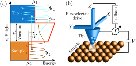
The most striking feature of this instrument is the remarkable spatial resolution it can achieve. The key for reaching a vertical resolution of a few hundredths of an Ångström is the exponential dependence of the tunneling current, , on the tip-to-sample spacing, :
| (1) |
For a typical metal ( eV) the current will decrease by about one order of magnitude for every Ångström increase in the electrode spacing. The lateral resolution mainly depends on the apex geometry and electronic orbitals of the scanning tip, which confine the tunneling electrons into a narrow channel, offering the unique opportunity to perform real-space imaging down to atomic length scales. Sec. III provides a more detailed discussion of the theoretical aspects of electron tunneling.
| Description | Experimental conditions | Specificities | Reference | ||
| 4He STMab | 1.6/4.2 K | ExGas | 8/10 T | cleavage and tip/sample exchange in UHV | Kent et al. (1992) |
| 4He STMa | 35 K–RT | UHV | – | in situ cleaving | Ikeda et al. (1993) |
| 4He STMc | 11–400 K | UHV | – | in situ tip/sample conditioning, 4He-flow cryostat | Horch et al. (1994) |
| 4He STMac | 7 K–? | UHV | 8 T | in situ tip/sample exchange, magnet lifted by bellow | Schulz and Rossel (1994) |
| 4He STMa | 1.5 K–RT | ExGas | 8 T | in situ tip/sample exchange | Tessmer et al. (1994) |
| 4He STMa | 4.2 K | ExGas | – | cold cleaving, magnetic coarse approach | Hancotte et al. (1995) |
| 4He STMc | 15 K–RT | UHV | – | in situ sample exchange | Meyer (1996) |
| 4He STMd | 8 K–RT | UHV | 7 T | split-coil, STM body pressed against conus | Wittneven et al. (1997) |
| 4He STMa | 11 K–RT | UHV | – | in situ tip/sample condition., top-loading with bellow | Foley et al. (2000) |
| 4He STMd | 16 K | UHV | 2.5 T | split-coil, in situ tip/sample exchange | Pietzsch et al. (2000) |
| 4He STM | 4–300 K | UHV | 8 T | rotatable field, STM cooled by superfluid 4He | Kondo et al. (2001) |
| 4He STMd | 6.5 K–RT | UHV | – | in situ tip/sample conditioning, 4He-flow cryostat | Zhang et al. (2001) |
| 3He STMd | 240 mK–RT | CryVac | 7 T | cold cleaving, in situ sample exchange | Pan et al. (1999) |
| 3He STMab | 275 mK–RT | UHV | 12/14 T | in situ tip/sample exchange, bottom-loading cryostat | Kugler et al. (2000) |
| 3He STMac | 260 mK–RT | L3He | – | top-loading, thermally compensated STM | Urazhdin et al. (2000) |
| 3He STMa | 500 mK–? | UHV | 7 T | in situ facilities, Joule-Thomson refrigerator | Heinrich et al. (2003) |
| 3He STMad | 315 mK–RT | UHV | 12/14 T | in situ tip/sample conditioning, spin-polarized STM | Wiebe et al. (2004) |
| ULT STM | 90 mK–RT | CryVac | – | ex situ sample preparation | Fukuyama et al. (1996) |
| ULT STM | 20 mK | UHV | 6 T | in situ tip/sample conditioning, bottom-load. cryostat | Matsui et al. (2000) |
| ULT STMb | 60 mK | CryVac | – | very compact design, rapid cool down | Moussy et al. (2001) |
| ULT STMb | 70 mK | CryVac | 12 T | home-built STM integrated into Oxford Kelvinox 100 | Upward et al. (2001) |
| System developed for the study of superconductors | |||||
| Based on coaxial inertial slider or ‘slip-stick’ design Lyding et al. (1988); Renner et al. (1990) | |||||
| Based on Besocke or ‘beetle’ design Besocke (1987) | |||||
| Based on ‘friction motor’ design Pan et al. (1999) | |||||
The tunneling regime is defined by a set of three interdependent parameters: the electrode spacing (typically 5–10 Å), the tunneling current (typically 0.01–10 nA), and the bias voltage (typically 0.01–2 V). The parameters and are generally chosen to set the tunneling resistance in the G range. It is worth mentioning that the absolute electrode spacing is not readily accessible by experiment: only relative variations can be measured. Another important point is that the measured tunneling current is a convolution of the electron densities of states of both the tip and the sample (Sec. III). To study intrinsic sample properties, it is therefore preferable to use tips with a featureless density of states and a well-defined Fermi surface (ideally spherical). The metals most commonly used for the tip are Au, W, Ir, and PtIr.222A selection of tip preparation techniques is discussed by Ekvall et al. (1999).
II.2 Technical challenges of low-temperature STM
A successful investigation of superconductors by STM relies essentially on three prerequisites: (i) a suitable sample surface; (ii) a scanning tunneling microscope allowing atomic resolution and stable spectroscopy; and (iii) an experimental environment featuring vacuum conditions, low and variable temperatures, as well as magnetic fields. This is a highly delicate endeavor, which requires the mastering of many technical challenges. In the following we briefly outline the major technical difficulties, and review some of the STM designs used to study superconductors at low temperatures (see Table. 1).
Controlling the sample surface quality is essential. Contamination in ambient atmosphere may rapidly degrade the sample top layer, often preventing stable and reproducible tunnel junctions and the investigation of intrinsic properties. This issue is non trivial and different for each compound, depending on its crystallographic structure and surface nature. The most suitable surfaces for STM/STS are those prepared in situ. Ideally, the top layers are mechanically removed by cleaving the sample in ultra-high vacuum (UHV), either at room temperature before cooling or at low temperature. This procedure works best for the more anisotropic layered compounds with a natural cleaving plane, such as Bi2212 Renner and Fischer (1994a); DeWilde et al. (1998); Pan et al. (2001), Bi2201 Kugler et al. (2001); Shan et al. (2003), Bi2223 Kugler et al. (2006), and Hg-compounds Rossel et al. (1994); Wei et al. (1998a).
Successful STM studies have also been reported for HTS which do not offer the advantage of a natural cleaving plane, such as Y123, Nd123 and the electron-doped superconductor NCCO Alff et al. (1998). In these cases, besides cleaving in UHV Edwards et al. (1992); Pan et al. (1999); Nishiyama et al. (2002), a number of successful experiments were carried out on as grown surfaces Maggio-Aprile et al. (1995) and surfaces prepared ex-situ by chemical etching Wei et al. (1998a); Shibata et al. (2003b) or by cutting using a razor blade Hayashi et al. (1998a).
Most low-temperature STMs described in this section are home-built and generally based on one of the following designs: the Besocke or ‘beetle’ setup Besocke (1987), the coaxial inertial slider or ‘slip-stick’ design Lyding et al. (1988); Renner et al. (1990) and the ‘friction motor’ Pan et al. (1999). A more complete description of the devices would go beyond the scope of this review: the interested reader may consult, for example, Güntherodt and Wiesendanger (1994).
The modern low-temperature STMs used for spectroscopic studies of oxide superconductors are generally mounted in a UHV chamber for the reasons mentioned above. The need for magnetic fields and ample cryogenic hold-time considerably increases the system complexity. The three main design challenges are (i) ensuring optimal vibration isolation to achieve high resolution and stable tunneling conditions, (ii) proper thermalization of the instrument to achieve low and stable temperatures, and (iii) confining the instrument inside the small bore of a superconducting coil. Table 1 provides a list of references for guiding the reader through the various existing low-temperature STM configurations developed to deal with these constraints.
The early low-temperature STMs were mostly based on conventional 4He cryostats working at K (in a few cases down to 1.5 K via a pumped 4He pot), generally cooled by exchange gas. Combining low temperatures and UHV leads to more complex systems, with the difficult task to properly thermalize the STM without coupling to mechanical vibrations. Optimal thermalization becomes even more important when sub-Kelvin temperatures and a variable temperature range are required. Moreover, for maximal flexibility and short turn-around times, an easy in-situ access to the STM for tip and sample exchange, as well as in-situ tip and sample conditioning, are necessary. Magnetic fields impose further considerable size and materials constraints: the STM has to be non-magnetic and has to fit into the coil.
In order to study ultra-low temperature phenomena with enhanced energy resolution, a few groups have developed sub-Kelvin systems, inserting the STM into 3He or dilution refrigerators. First STS studies in small fields below 1 K were achieved by Hess et al., with the historical imaging of individual Abrikosov vortex cores in NbSe2, first at 300 mK using a 3He refrigerator Hess et al. (1990) and later at 50 mK in a dilution fridge Hess et al. (1991). Other groups followed and added higher magnetic fields and/or UHV conditions with in situ facilities. Compared to 3He refrigeration, dilution refrigeration offers the advantage of reaching temperatures of the order of 50 mK. However, the thermalization of the sample and STM below 100 mK is difficult, making the operation in a dilution refrigerator much more complex.
II.3 Operating modes
A scanning tunneling microscope allows to collect topographic and spectroscopic data on a local scale. In the topographic mode, the surface is mapped via the dependence of the tunneling current upon the tip-to-sample distance. In spectroscopy, the LDOS of the material is extracted through measurements of the tunneling conductance.
II.3.1 Topography
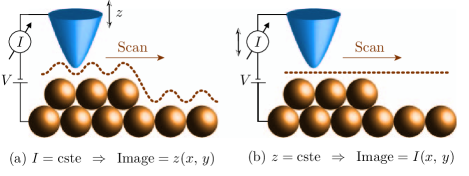
Constant-current imaging
(Fig. 2a) In this standard mode, the tunneling current is kept constant by continuously feedback-adjusting the tip vertical position during the scan. Since the tunneling current integrates over all states above or below , up to an energy equal to the tunnel voltage (Sec. III), the constant-current mapping corresponds to a profile of constant integrated electron density of states (DOS). If the LDOS is homogeneous over the mapped area, this profile corresponds to constant tip-to-sample spacing, and recording the height of the tip as a function of position gives a three dimensional image of the surface . Because the tip follows the corrugations of the surface at a constant spacing, the scan speed is limited by the feedback loop bandwidth, which is typically in the kilohertz range.
Constant-height imaging
(Fig. 2b) In this mode the tip is scanned over the sample surface while maintaining the tip at a constant absolute height (feedback loop turned off). For ideal tip and sample, modulations of the tunneling current are only due to variations in the tip-to-sample spacing, and recording the current as a function of position will reflect the surface topography. This mode allows fast scanning, but is restricted to surface areas where the corrugations do not exceed a few Ångströms, to avoid tip collisions with large surface protrusions. According to Eq. (1), the image corrugation depends on the local work function as . Thus, unless the actual local value of is known, quantitative characterizations of topographic features are difficult to achieve.
II.3.2 Local tunneling spectroscopy
Locally resolved electron spectroscopy is probably the most sophisticated application of the STM. The electronic density of states can be accessed by recording the tunneling current while the bias voltage is swept with the tip held at a fixed vertical position. If a positive bias voltage is applied to the sample, electrons will tunnel into unoccupied sample states, whereas at negative bias they will tunnel out of occupied sample states (Fig. 1a). Although the interpretation of spectra can be quite complex, it can be shown that in ideal conditions the tunneling conductance provides a valid measurement of the sample LDOS [see Eqs. (4) and (6)]. This straightforward way to interpret the experiments is used in most STM/STS studies.
spectra can either be obtained by numerical differentiation of curves or by a lock-in amplifier technique. In the latter case, a small ac-voltage modulation is superimposed to the sample bias , and the corresponding modulation in the tunneling current is measured. Expanding the tunneling current into a Taylor series,
one finds that the component at frequency is proportional to . This statement is only valid if and if is sufficiently smooth. For optimal energy resolution, should not exceed , and typical values are in the few hundred range. The advantage offered by the lock-in technique is that the sampling frequency can be selected outside the typical frequency domains of mechanical vibrations or electronic noise, considerably enhancing the measurement sensitivity.
II.3.3 Spectroscopic imaging
Most STS experiments use ‘current-imaging tunneling spectroscopy’ (CITS), introduced by Hamers et al. (1986). A CITS image is based on a regular matrix of points distributed over the surface. The tip is scanned over the sample surface with a fixed tunneling resistance , recording the topographic information. At each point of the CITS array, the scan and the feedback are interrupted to freeze the tip position (, , and ). This allows the voltage to be swept to measure and/or , either at a single bias value or over an extended voltage range. The bias voltage is then set back to , the feedback is turned on and the scanning resumed. The result is a topographic image measured at , and simultaneous spectroscopic images reconstructed from the and/or data. Because the feedback loop is interrupted, can take any value, even those where . This technique provides a very rich set of information.
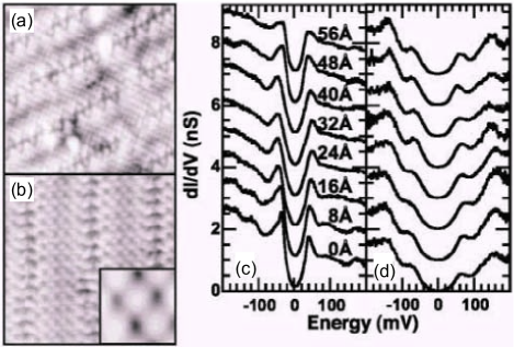
For best contrast in the spectroscopic images it is important to select the energy where maximal variations in the tunneling conductance occur. In the case of vortex imaging (Fig. 3) the mapping energy is usually selected at the position of the coherence peaks (superconducting gap), or close to zero energy where the amplitude of the localized core states is largest (Sec. VII). This technique also enables to reconstruct spectroscopic maps acquired simultaneously at different energies. An example of such analysis was provided by Hess et al. (1991) who measured the energy dependence of the star-shaped vortex core structure in NbSe2, and by Pan et al. (2000a) who used Fourier transforms of such maps on Bi2212 to reveal periodic modulations of the LDOS in real space (Sec. VIII). From the energy dependence of these modulations, energy dispersion curves could be extracted, opening to STS the door of reciprocal-space spectroscopies.
III The theory of electron tunneling
The theory of tunneling began in the first years of quantum mechanics, and now covers a large variety of experimental situations.333See for example Duke (1969), Wolf (1985), and the series edited by Wiesendanger and Güntherodt (1993). The interpretation of most tunneling measurements on high- superconductors is based on the tunneling-Hamiltonian formalism, which we shortly describe in Sec. III.1 and present in more detail in Appendix A. In Sec. III.2 we mention some of the more sophisticated approaches to electron tunneling which have been developed over the years. Sec. III.3 is primarily dedicated to the often overlooked question of the tunneling matrix element, with a particular emphasis on the case of local vacuum tunneling (STM junction). Finally, in Sec. III.4 we formulate some issues in the theoretical interpretation of the tunneling experiments on HTS.
III.1 The tunneling Hamiltonian formalism
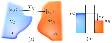
Like any transport process, the tunneling of electrons across a vacuum or insulating barrier is a non-equilibrium phenomenon, and the injected quasiparticles are not a priori in thermal equilibrium with the lattice. In the STM experiments, however, the amplitude of the current is so low that the time between two tunneling events is much longer than the typical quasiparticle relaxation time. In this situation it is appropriate to use an equilibrium theory; it is also reasonable to assume that the correlations play no role in the barrier and that the elementary process involved is the tunneling of a single electron. When the two metals are superconductors, the coherent tunneling of a Cooper pair can also take place, leading to the celebrated Josephson effect Josephson (1962).
The tunneling-Hamiltonian formalism Bardeen (1961); Cohen et al. (1962); Bardeen (1962) provides a framework to understand both the single-particle and the pair tunneling phenomena. The two materials forming the tunnel junction are considered as two independent systems (Fig. 4). The transfer of particles across the barrier is described by the phenomenological ‘tunneling Hamiltonian’
| (2) |
We use the index to label the single-particle states on the left side of the junction, and the index for the states on the right side. The operator destroys a particle in the state and the operator creates a particle in the state . The quantity is known as the ‘tunneling matrix element’. It mainly depends upon the geometry of the tunnel junction, but also on the details of the electronic states on both sides. The proper definition and the explicit evaluation of are difficult problems which have stimulated a lot of work, especially in the case of the STM junction. We shall discuss the tunneling matrix element further in Sec. III.3.
If the bias applied across the junction is small, the current can be calculated using linear-response theory (see Appendix A.1). The total current turns out to be the sum of two contributions, and . The first part is the single-particle current and is given by
| (3) |
where and are the single-particle spectral functions of the (isolated) left and right materials, respectively, and is the Fermi function. Eq. (3) applies to any type of tunnel junction. The most common cases, planar and STM junctions, will be discussed shortly. The meaning of Eq. (3) is obvious: the Fermi factors select the energy window where occupied states in one material, say on the left, can be aligned with empty states on the right; within that window, an electron in a state can tunnel into an empty state if the two states are connected by a non vanishing matrix element, and if they are aligned in energy by the applied bias. Eq. (3) can also be rationalized within the simple ‘semiconductor model’ Nicol et al. (1960); Tinkham (1996). We shall not consider in this review the second contribution to the current, , which describes the coherent tunneling of electron pairs.444The observation of the Josephson current by STM using a superconducting tip is challenging because it requires a relatively low junction resistance. This type of experiment has not been reported so far for the HTS, but was recently achieved with conventional superconductors Naaman et al. (2001); Naaman and Dynes (2003, 2004); Suderow et al. (2002); Martinez-Samper et al. (2003); Rodrigo and Vieira (2004).
The main strength of Eq. (3) is its generality: it applies to any tunnel junction, provided that the tunneling takes place at energies lower than the barrier height, and that high-order effects in (such as interferences occurring within the barrier) are not important. Surface and geometric effects are in principle embodied in the spectral functions and in the matrix element. In practice one often assumes that the surface disruption does not change significantly the electronic properties, and that the spectral functions entering Eq. (3) can be identified with the bulk ones.
The explicit appearance of the spectral functions in Eq. (3) is another appealing feature of this formalism, which opens the door for tunneling spectroscopy. Consider a junction between a simple metal with a structureless DOS on the left—the probe—and a given material on the right—the sample. In general, the tunneling matrix element depends upon the electron quantum numbers (see Sec. III.3), but for the sake of the argument we assume here that it is a constant: . Then at zero temperature Eq. (3) leads to the following expression for the tunneling conductance:
| (4) |
where and denote ‘left’ and ‘right’ and is the DOS measured from the Fermi energy. This simple formula shows the essence of tunneling spectroscopy: the bias dependence of the tunneling conductance directly probes the DOS of the sample. This result is not valid in general, however, as discussed at length in Sec. III.3. The correspondence between the tunneling conductance and the sample DOS, first postulated by Giaever (1960), was the initial motivation for the Bardeen (1961) tunneling theory.555 For SIS junctions, i.e. junctions involving two superconductors separated by a thin insulating barrier, Eq. (3) and the assumption yield a partial convolution of the materials’ DOSs instead of the DOS itself, that is at zero temperature.
For understanding local probes like the STM, it is helpful to express Eq. (3) in terms of the real-space spectral function, which is closely related to the LDOS (Appendix A.1). Tersoff and Hamman (1983) performed the first calculation of the tunneling matrix element for the STM junction, and found an explicit relation between the tunneling current and the sample LDOS :
| (5) |
where denotes the tip center of curvature (Appendix A.2). Assuming a structureless tip DOS, , Eq. (5) gives
| (6) |
where is the derivative of the Fermi function. Thus the interpretation of scanning tunneling spectroscopy becomes remarkably simple: the voltage dependence of the tunneling conductance measures the thermally smeared LDOS of the sample at the position of the tip. Because the local tunneling matrix element is properly taken into account, Eq. (6) describes the STM much better than Eq. (4) describes planar junctions.
III.2 Other approaches to the tunneling problem
The success of the tunneling-Hamiltonian formalism in describing many experimental results, in particular the Josephson effect, led several authors to investigate this approach in depth. One of the first questions raised concerned the primary assumption of the theory, namely the possibility to represent the junction as two independent systems coupled by a term like . Not surprisingly it was found that this assumption is not valid in general Prange (1963); Zawadowski (1967); however the associated error turned out to be small. The effect of interactions in the electrodes and in the barrier was also investigated Schrieffer (1964); Scalapino et al. (1966); Appelbaum and Brinkman (1969a, b); Duke (1969); this allowed, in particular, to explain the fine structure of the conductance in BCS superconductors in terms of the phonon spectrum McMillan and Rowell (1965). The most significant improvements on the original theory are perhaps the incorporation of non-equilibrium effects by means of the Keldysh formalism Caroli et al. (1971); Feuchtwang (1974), as well as the non-perturbative treatments Noguera (1990); Sacks and Noguera (1991), which gave useful information on the accuracy of the perturbative approach. The resulting theories are rather complicated, and were not yet used in the context of the high- superconductors.
In order to avoid difficulties inherent to the tunneling-Hamiltonian formalism, and for treating the regime where the interaction between the two materials cannot be neglected, several authors proposed approaches based on the scattering theory Lucas et al. (1988); Doyen et al. (1993); Cuevas et al. (1996); Ness and Fisher (1997); Carminati and Sáenz (2000), in the spirit of the Büttiker et al. (1985) transport theory. For superconducting junctions, the most popular method is due to Blonder et al. (1982). Initially developed for planar junctions involving a BCS -wave (or -wave, Tanaka et al., 1995) superconductor, this approach was nevertheless occasionally used to interpret STM spectra on HTS materials.
Another approach was explored by Lang (1985), who represented both tip and sample by a single atom adsorbed on a jellium surface, and calculated the tunneling current using a first-principles method. This study illustrated the atomic character of the STM junction, which in effect can be viewed as an atom-to-atom contact (see also Tsukada et al., 1993), and initiated many subsequent works based on the ab initio methods (see, e.g. Ciraci and Batra, 1987; Tersoff, 1989; Hofer et al., 2001, 2003).
III.3 The tunneling matrix element
In the Bardeen (1961) theory the matrix element is the expectation value of the single-particle current in the direction normal to the plane of the junction, through a surface lying entirely in the barrier region:
| (7) |
Duke (1969) and Wolf (1985) give comprehensive reviews of the various models for developed prior to the invention of the STM. Hereafter we describe the most popular models for planar and STM junctions.
III.3.1 The planar junction
has a particularly simple form at ideal planar junctions, due to conservation of momentum in the plane parallel to the interface Harrison (1961); Duke (1969); Wolf (1985). The exponential decay of the wave functions in the barrier leads to an exponential dependence of on the barrier thickness , which reduces to in the limit of a wide and square barrier; is the electron momentum in the barrier and is the energy for the motion normal to the interface, measured from the top of the barrier. This exponential factor suggests that the tunneling current is dominated by states with a large velocity along the direction, and consequently a small momentum in the plane, leading to a momentum selectivity often referred to as the ‘tunneling cone’ Beuermann (1981). The matrix element is also proportional to the group velocity along Harrison (1961). In Eq. (3), however, this velocity factor is canceled by an equivalent DOS factor. A counterintuitive consequence of this cancellation is the possibility to tunnel along the axis into a quasi two-dimensional material (without dispersion along ), in spite of the low conductivity in the direction. This latter property would imply that -related DOS features should not show up at all in the planar tunneling spectra Harrison (1961), in sharp contrast with the simple result of Eq. (4), and with the experimental observation of the superconducting DOS by Giaever. Bardeen (1961) attributed this discrepancy to the fact that the electrons are not paired in the barrier region; thus the velocity entering would be the velocity of the bare electrons rather than the quasiparticle velocity , and the superconducting gap would show up in the tunneling spectra, although the normal-state DOS would not.
It should be noted that these arguments apply to materials with spherical Fermi surfaces and isotropic superconducting gaps, and must be reconsidered when dealing with the cuprate superconductors. As pointed out by Wei et al. (1998a), the tunneling cone “flattens out” for -axis tunneling into the plane of the HTS, because is almost independent of the in-plane momentum. Therefore one expects to measure the -plane band structure in the planar -axis tunneling spectra of the HTS.
III.3.2 The STM junction
Because of the lateral confinement, the one-electron states of the STM tip cannot be characterized by a single momentum in the plane, which makes the calculation of the tunneling matrix element more difficult than in the planar junction case. Soon after the invention of the STM, Tersoff and Hamman (1983, 1985) proposed an expression for , which is still widely used to interpret STM images. They represented the tip apex by a spherical potential well and found that Bardeen’s matrix element Eq. (7) is proportional to the sample wave function at the center of the tip apex:
| (8) |
Using Eq. (8) they were able to explain the measured corrugations for the various superstructures observed on the reconstructed Au (110) surface. The case of a non-spherical tip and a rough sample surface was later treated along the same lines Sacks et al. (1988); Šestović and Šunjić (1995). In these models the atomic structure of the tip is not taken into account. This issue was investigated by Chen (1988, 1990a, 1990b), who assumed instead that a single atom at the tip apex is responsible for the interaction with the sample surface. Chen summarized his results in a ‘derivative rule’: is proportional to a derivative of the sample wave function, which derivative depends upon the orbital state of the apex atom. Eq. (8) can be regarded as a particular case appropriate for -wave tips. The unexpectedly large corrugation amplitudes observed on HTS surfaces could possibly be explained using this formalism.
According to Eq. (8) and the resulting Eq. (5), the -axis STM tunneling into a nearly two-dimensional material is possible, like for the planar junction, but for different reasons. On the one hand the local nature of the STM tip explains its ability to measure all momenta in the plane, thus preventing any momentum selectivity. On the other hand in Eq. (8) is not proportional to the group velocity along , in contrast to the planar junction case. The complete absence of a velocity factor in Eq. (8) results from specific approximations made by Tersoff and Hamman, such that having a spherical tip wave function and identical work functions in the sample and the tip; the relaxation of these assumptions would yield some dependence upon the group velocity, but is not expected to change the picture qualitatively.
III.4 Interpretation of STM experiments on HTS
A consistent interpretation of the STM experiments on HTS must address two different questions. The first concerns the electronic nature of the materials themselves, and the second is the coupling of the material surfaces with the STM tip. Until now theorists have focused on the former problem, and made considerable progress; several excellent reviews of this effort were given recently.666Dagotto (1994); Anderson (1997); Orenstein and Millis (2000); Chubukov et al. (2003); Norman and Pépin (2003); Sachdev (2003); Kivelson et al. (2003); Carlson et al. (2004); Lee et al. (2004); Demler et al. (2004). This is not an exhaustive list. In this paragraph we leave this question aside, and we address some issues related to the tunneling process itself, concentrating on the Bi2212 compound.
Generally the conditions of the STM measurements on HTS are consistent with the basic assumptions of the tunneling-Hamiltonian theory. The absence of a substantial interaction between tip and sample was evidenced by the insensitivity of the tunneling conductance to the tip-sample distance Renner and Fischer (1995). The interval between two tunneling events is typically s for a current of nA, which is long compared to the relaxation times s in the materials; therefore non-equilibrium effects are not expected to play a role in STM spectra.
III.4.1 The role of the BiO surface layer
Many STM experiments on Bi2212 have been successfully interpreted using Eq. (6). It is commonly believed that the measured LDOS originates from the CuO2 bilayer (see Fig. 5). According to Eq. (6), though, the LDOS is not measured directly on a CuO2 plane, but at some point typically 10 Å above that plane, since Bi2212 cleaves between the weakly bonded BiO sheets. The CuO2 layer lies 4.5 Å beneath the surface BiO layer, raising the question of the role played by the BiO in the tunneling process from the STM tip to the CuO2. That the BiO indeed plays a significant role is obvious from the topographic images, which show the lattice of Bi atoms on the surface (see Sec. IV.1).
The band calculations indicate that the BiO layer is metallic.777Hybertsen and Mattheiss (1988); Massidda et al. (1988); Krakauer and Pickett (1988); Herman et al. (1988); Mattheiss and Hamann (1988); Szpunar and Smith (1992); Jarlborg and Santi (2000) This result contradicts the common experimentalist’s wisdom that the BiO layer is insulating. The metallic nature of BiO in these calculations is due to a pair of conduction Bi()-O() hybrids, which disperse below the Fermi energy in a small region around the point of the Brillouin zone. It is well known that correlation effects on the Cu() orbitals lead to a failure of the LDA approaches in the antiferromagnetic phase; such effects are not expected in the BiO layer. Therefore, a Bi-O band at the Fermi surface would give rise to a sharp peak in the spectral function near . This peak is not seen in ARPES experiments Damascelli et al. (2003); Campuzano et al. (2004), suggesting that the Bi-O band indeed lies above . Singh and Pickett (1995) found that in Bi2201 the calculated Bi-O bands move upward by meV when the distortion of the BiO planes is taken into account. Very recently, Lin et al. (2006) found that a similar shift occurs in Bi2212 when lead or oxygen doping is introduced in the calculation.
If the BiO surface layer is not conducting, then at sufficiently low energies the STM would necessarily measure the spectral properties of the buried CuO2 bilayer. The observation of the Bi lattice in the topographic images could then be due to e.g. (i) a modulation of the shape of the tunnel barrier by the Bi atoms, (ii) a diffraction of the tunneling electron by the BiO (and SrO) intermediate layers, (iii) the admixture of some Bi() character in the Cu()-O() states of the CuO2 bilayer, (iv) the fact that the bias applied to record the topography (typically V) would lie within the Bi-O bands.
III.4.2 Momentum dependence of the matrix element
The matrix element Eq. (8) is local in space [see also Eq. (25)]. In some instances, especially in the context of STM tunneling on impurities (Sec. V.5), it has been claimed that the matrix element could be non local, i.e. could depend upon the sample wave function in some vicinity of the tip position . A phenomenological generalization of Eq. (8) taking into account this possibility would be
| (9) |
The function weights the various contributions of the sample wave function around the tip, and reduces to for a local matrix element. For a translationally invariant system, Eq. (9) leads to (Appendix A.3):
| (10) |
where is the Fourier transform of and is the sample spectral function.888The assumption of translational invariance excludes from the outset any atomic-scale dependence of the tunneling conductance. Hence Eq. (10), unlike Eq. (6), cannot address the question of the atomic resolution or describe inhomogeneous systems like vortex cores. Eq. (28) provides the suitable generalization of Eq. (6) to account for a non-local matrix element. The vector in Eq. (10) belongs to the three-dimensional Brillouin zone of the sample. In the case of the HTS, though, the dependence of the spectral function can be to first approximation neglected, and the sum does not contribute to the dependence of . Anisotropic matrix elements have been invoked for the interpretation of various experimental results as discussed in Secs. IV.1.2, V.5, VII.2.2, and VII.4.
The STM measurements on zinc impurities in Bi2212 (Pan et al., 2000b, see Sec. V.5) revealed a sharp maximum in the LDOS at the impurity site. Similar spectra were observed on surface defects Yazdani et al. (1999). These observations contrast with the prediction of the BCS theory in the unitary limit, namely a vanishing LDOS on the impurity and resonances on the neighboring sites Salkola et al. (1996). Martin et al. (2002) argued that the tunneling into the planar Cu() orbitals occurs indirectly through Cu or Bi orbitals extending out of the surface and having zero in-plane orbital momentum. As a result the STM would not probe the wave function at the Zn site, but at the four neighboring Cu sites (see Fig. 18). The weighting function in Eq. (9) would then take the form , where and are the basis vectors of the Cu lattice. The opposite signs along the and directions reflect the symmetry of the CuO2 orbitals near . In the reciprocal space this corresponds to . The absence of a large zero-bias conductance peak in the vortex cores was also tentatively attributed to matrix-element effects (Wu et al., 2000, see Sec. VII.2.2). In the STM literature, this matrix element is often attributed to Chakravarty et al. (1993), although these authors introduced it for describing the coherent tunneling of Cooper pairs in bilayer compounds. Franz and Tešanović (1999) obtained the same result for a planar-junction, after summing over the momenta along the axis, and argued that this matrix element would prevent the STM from seeing the Doppler-shift induced zero-energy DOS in the mixed state (Volovik, 1993, see Sec. VII.4). Finally a similar form for (with a plus sign instead of the minus sign) was also suggested by arguing that direct tunneling into the planar CuO2 orbitals is blocked by the atomic cores in the intermediate SrO and BiO layers Zhu et al. (2000).
The anisotropic matrix element would prevent the electrons from tunneling into states with momenta along the nodal directions, and would therefore highlight the region of the Brillouin zone. For a homogeneous -wave superconductor the low-energy conductance resulting from Eq. (10) with an anisotropic would show a rounded U-shape instead of the V-shape characteristic of nodal quasiparticles. However, after a detailed fit of the Bi2212 data, Hoogenboom et al. (2003a) concluded that the low-energy conductance is incompatible with an anisotropic matrix element. The recent observation that the STM spectra measured directly on the CuO2 layer exhibit a U-shape, while the spectra taken on the BiO layer have the -wave V-shape (Misra et al., 2002a, see Sec. IV.1.2), was attributed by the authors to a different matrix element in the two tunneling configurations.
The actual form of the matrix element for STM tunneling into HTS remains largely controversial.999Some authors analyzed tunneling spectra on HTS using a matrix element analogous to the one derived by Harrison for planar junctions, Kouznetsov and Coffey (1996) or Yusof et al. (1998). The main motivation was to explain the absence of some sharp structures, such as van-Hove singularities, in the experimental tunneling spectra, and the observed asymmetry in the background conductance (Sec. V) as well as specific features observed in point-contact tunneling experiments. Here is the group velocity and is a function selecting the momenta close to the tunneling direction, which was introduced by Ledvij and Klemm (1995) as a generic model for the Josephson coupling between planar superconductors. The validity of these planar-junction matrix elements to account for the STM and point-contact geometries was not addressed, however. Since no direct experimental determination of (or ) has been possible so far, and no microscopic calculation of the tip/surface system has been reported, most assessments about the matrix element rely upon phenomenological or heuristic arguments. The V-shaped spectra acquired on the BiO layer support the idea of a Tersoff and Hamman-like matrix element, i.e. . Although there is no compelling experimental evidence in favor of an anisotropic , the measurements on zinc impurities and possibly also on vortices could be interpreted in the framework of the BCS theory assuming a more complicated matrix element like . However, alternate explanations which emphasize the non-BCS character of the HTS have also been proposed.
III.5 Summary
Most STM spectroscopic measurements on HTS have been successfully analyzed in the framework of the tunneling-Hamiltonian formalism. Complemented with the Tersoff and Hamman treatment of the STM junction, this formalism provides a straightforward interpretation of the tunneling data, Eq. (6), in terms of the sample LDOS. Although there is a broad consensus regarding this interpretation of the data, a definitive assessment requires to fix the issue of the tunneling matrix element.
IV Crystal structure and surface characterization
The superconducting gap of standard isotropic BCS superconductors is independent on position in real space and on momentum along the Fermi surface in -space (-wave gap symmetry). Therefore, the tunneling spectra of a homogeneous sample neither depend on the tunneling direction, nor on the position along the surface, nor on the chosen surface. Under those circumstances the measured gap does not depend upon the above-mentioned experimental configuration, allowing for an unambiguous interpretation of tunneling experiments. The situation is very different in layered HTS cuprates, owing to their very anisotropic structural, electronic, and superconducting properties.
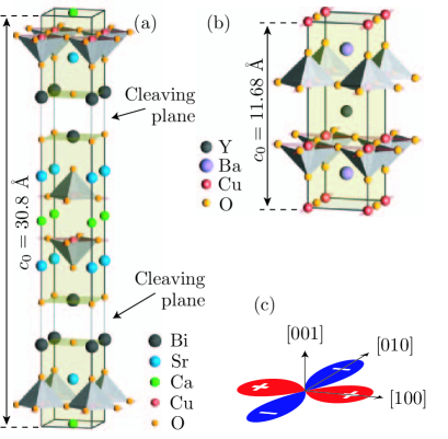
The HTS cuprates consist of one or more superconducting copper oxide (CuO2) sheets sandwiched between non-metallic charge reservoir layers (Figs. 5a,b). Because of the alternate stacking of superconducting and non-superconducting layers along the crystallographic direction, the tunneling spectra of surfaces are likely to depend on the termination layer. As a result of the -wave symmetry (Fig. 5c) of the superconducting gap, the spectra may also strongly depend on which momentum states contribute to the tunneling current (see Sec. III.4.2). Finally, the sign change of the -wave gap function at the nodal points along induces quasiparticle bound states at surfaces or step edges oriented perpendicular to the nodal directions. The spectroscopic signature of these bound states is an enhanced conductance—so called zero-bias conductance peak—instead of a gap at Kashiwaya and Tanaka (2000). For all these reasons, tunneling spectra measured on HTS are likely to depend on the exposed surface layer, its orientation, and the details of the tunneling matrix element. Hence, a range of different tunneling spectra is expected, even for perfect vacuum tunnel junctions, making their interpretation very challenging.
On layered HTS, such as Bi2Sr2CaCu2O8+δ, a further key issue is to identify which states are being probed by STM. Does the tunneling current involve pure BiO or CuO2 derived states, or some hybridized ones? This question, which we already touched upon in Sec. III, is of fundamental importance. Superconductivity is believed to reside in the CuO2 plane, but most tunneling measurements of the superconducting -wave gap were obtained on the BiO surface. Ascribing the measured gap to the superconducting state of HTS, implies that tunneling into the BiO surface allows to measure the superconducting gap of the CuO2 layer situated several Ångströms beneath the surface. This statement is far from obvious because of the short coherence length in HTS and the non-metallic layers sandwiching the superconducting CuO2 sheets. The possibility to sense electronic contributions from sub-surface atomic layers is well known in highly ordered pyrolytic graphite, a very simple layered conductor. STM images of this material reveal two non equivalent carbon sites instead of a regular honeycomb lattice Wiesendanger and Anselmetti (1992), due to site-dependent hybridization of carbon orbitals from the neighboring graphene sheet.
A careful assessment of the probed surface and of the tunnel junction is prerequisite to lift the above ambiguities and enable a meaningful interpretation of the tunneling spectra measured on HTS. Identification of the local surface layer is best done through atomic-scale imaging. However, such optimal resolution remains elusive on most HTS cuprates, and in Secs. IV.1 and IV.2 we restrict the discussion to the archetypical Bi- and Y-compounds, respectively. The quality of the tunnel junction can be inferred from the reproducibility of the spectra as a function of position along the surface and as a function of tip-to-sample distance as discussed in Sec. IV.3.
IV.1 Surfaces of Bi-based cuprates
Bi2Sr2CaCu2O8+δ (Bi2212) is the most widely studied HTS using STM for a simple reason: it is straightforward to prepare atomically flat and clean surfaces by cleaving. Cleaving is most likely to occur between the weakly van der Waals coupled adjacent BiO layers (Fig. 5a), and with few exceptions, STM studies have focused on BiO terminated surfaces. It was the first surface of any HTS to yield STM images with atomic-scale topographic resolution. Following the pioneering work by Kirk et al. (1988), the resolution steadily improved to reveal the tetragonal unit cell and the incommensurate supermodulation along with stunning sharpness.
Cleaving predominantly exposes the BiO layer to the surface. However, other surface terminations were occasionally observed by STM Murakami and Aoki (1995); Pan et al. (1998b); Misra et al. (2002a). In the following paragraphs, we discuss STM investigations of the BiO and CuO2 surfaces in greater details.
IV.1.1 BiO surface
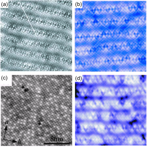
The structural characteristics of the BiO surface, as seen by STM, are similar in all parent Bi-based HTS cuprates (Figs. 6a,b). Distinctive features include a nearly commensurate supermodulation along and concomitant dark-atom rows running along the supermodulation ridges. The supermodulation develops throughout the bulk BiO layers, and is not a surface effect Heinrich et al. (1994); Gladyshevskii and Flükiger (1996). Note that the supermodulation along in Bi2212 is mostly structural. No associated spatial variation of the superconducting gap amplitude has been reported. The dark-atom rows are observed on all pure BiO surfaces except in few instances on Bi2201 Inoue et al. (1995) and Bi2212 Shih et al. (1991).
The origin of the supermodulation and the dark-atom rows is still matter of debate. Initially interpreted as rows of missing atoms Kirk et al. (1988), the latter were recently found to be more consistent with depressed rather than vacant lattice sites. Inoue et al. (1994) attributed them to spatial ordering of non equivalent Bi atoms, whereas Zandbergen et al. (1998) ascribed them to extra oxygen in the BiO layers. The supermodulation could result from a structural mismatch among the constituent layers of Bi2212. Based on X-ray refinement, Gladyshevskii et al. (2004) propose an alternative model where it stems from a rotation of Bi-O trimer in the BiO plane. In this scenario, the dark-atom rows reflect additional oxygen atoms necessary to register this rotation to the BiO lattice. Gladyshevskii et al. further observe that this additional oxygen site is quenched in lead-doped Bi2212, suppressing both the supermodulation and the dark-atom rows, consistent with STM topographs of lead-doped Bi2212 (Fig. 6c).
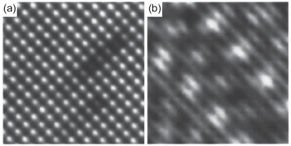
The BiO layers contain two atomic species, but atomic-scale STM images reveal only one lattice site. Shih et al. (1991) found no dependence on bias polarity or amplitude as would be expected if the BiO layer was an ionic insulator, suggesting a single atomic species is contributing to the contrast. Strong indications that STM is imaging the Bi lattice come from studies of Pb Kinoda et al. (2003), Zn Pan et al. (2000b), and Ni Hudson et al. (2001) substituted single crystals. In the case of lead doping, images of the BiO surface reveal some brighter lattice sites due to the dopant atoms (Fig. 6c). Lead substitutes for bismuth in the BiO layer, hence the STM imaging contrast shows the bismuth lattice. Zinc and nickel substitute for copper in the CuO2 layer. Unlike lead dopant atoms, the latter are not directly resolved in topographic images (Fig. 6d). However, they are clearly seen at the bismuth lattice sites in spectroscopic images of the surface (i.e. spatially resolved maps of the local tunneling conductance, see Figs 18 and 19). Since the bismuth and copper lattices are aligned along the direction, the implication is again that STM topographs of the BiO surface do reveal the bismuth lattice. Moreover, the latter results show that tunneling into the BiO surface feels the underlying CuO2 plane, supporting the idea that the superconducting gap of the CuO2 layer can be measured by tunneling into the BiO surface.
IV.1.2 CuO2 surface
The most comprehensive topographic and spectroscopic STM study of the CuO2 surface to date was carried out by Misra et al. (2002a) on Bi2212 thin films. They clearly resolved the tetragonal lattice of the CuO2 and the BiO surfaces (Fig. 7). Both layers host a supermodulation of similar periodicity with one characteristic difference: the in-plane concomitant lattice modulation is much weaker in CuO2 layers than in BiO layers Gladyshevskii and Flükiger (1996). While they obtain tunneling spectra of the BiO surface consistent with a -wave superconducting gap (Fig.7c), CuO2 terminated surfaces show a wider gap ( meV) with a strongly suppressed conductance near the Fermi energy (Fig.7d). This U-shaped energy dependence of the CuO2 tunneling conductance close to (Fig.7d) is unexpected for a -wave superconductor, raising the question of the electronic nature of a bare CuO2 layer. Kitazawa et al. (1996) already noted the tendency of CuO2 surfaces to yield spectra with a U-shaped energy dependence at low bias (expected for a -wave BCS gap), whereas other surface terminations of HTS cuprates show a V-shaped energy dependence near (expected for a -wave BCS gap).
The electronic structure of the BiO layer is likely to be the same at the surface and in the bulk, because cleaving between adjacent BiO layers does not break any strong bond. Exposing the CuO2 layer to the surface is significantly more disruptive, hence its structural and electronic properties may be very different from the bulk. Misra et al. (2002a) ruled out any surface reconstruction to explain the non -wave CuO2 spectra, because the measured surface structure (Fig. 7b) matches the bulk structure Heinrich et al. (1994); Gladyshevskii and Flükiger (1996). The large gap revealed by spectroscopy may signal an insulating CuO2 surface. But Misra et al. contend it would have to be a very homogeneous insulator, with an electron-hole symmetric low energy DOS and lying exactly half way between the empty and filled bands (Fig. 7d).
Misra et al. (2002a) argue that the -wave looking spectra they measured are consistent with -wave superconductivity in the CuO2 planes, provided the tunneling matrix element is of the anisotropic form (see Sec. III.4.2). This particular choice of enables them to reproduce the gap structure and the conductance peaks below meV. Their fit yields a gap amplitude consistent with a reduced doping, possibly due to oxygen loss and asymmetric doping by the BiO layer underneath: meV is indeed close to the gap measured in highly underdoped, yet superconducting samples Zasadzinski et al. (2001). The analysis by Misra et al. implies that the bare CuO2 layer at the surface is superconducting, which is an important finding. However, their model only partially reproduces the experimental spectra of CuO2. In particular, it does not account for the higher energy peak structures, and does not exclude the possibility that the CuO2 spectra reflect some signature of the pseudogap (Sec. VI). Finally, they do not answer the question as to why of BiO and CuO2 surfaces would be so different, leaving the nature of the CuO2 surface open to further investigations.
IV.2 Surfaces of YBa2Cu3O7
YBa2Cu3O7 (Y123) is the second most studied HTS by STM. Y123 is much less anisotropic than Bi2212 and offers no natural cleaving plane. STM experiments were carried out on as grown and chemically etched surfaces, as well as on single crystals cleaved at low temperature ( K). Y123 cleaves between the BaO and CuO-chain layers, and both were imaged with atomic resolution STM on low-temperature cleaved samples Edwards et al. (1994); Pan et al. (1999). The problem with cleaved specimens is that STM Edwards et al. (1992) and ARPES Campuzano et al. (1990) experiments degrade if the surfaces are not kept below 70 K, indicating they are unstable and possibly different from the bulk due to mechanical strain and unbalanced charges.
On the other hand, reproducible temperature-dependent STM spectroscopy was demonstrated on as grown surfaces of single crystal grown in BaZrO3 crucibles Maggio-Aprile et al. (2000). These surfaces could sustain repeated thermal cycling between 4 K and 300 K. They also allowed the first successful imaging of the Abrikosov vortex lattice in a HTS Maggio-Aprile et al. (1995). Similar results have been achieved on chemically etched surfaces Shibata et al. (2003b); Wei et al. (1998b). Atomic resolution on as-grown Y123 surfaces appears very difficult to achieve and has been reported only on thin films Lang et al. (1991); Nantoh et al. (1995). A reliable recipe allowing both atomic-resolution imaging and reproducible spectroscopy over a wide temperature range on Y123 has yet to be found.
The orthorhombic lattice of BaO terminated low-temperature cleaved surfaces has been clearly resolved by STM (Fig. 8a), with a few single atomic defects attributed to oxygen vacancies Pan et al. (1999). Similar micrographs were obtained by Edwards et al. (1994) who found them to be independent of bias amplitude and polarity, although a systematic energy dependence is not available yet.
CuO-chain terminated surfaces have been investigated in greater details. They show a more complex structure with a large charge modulation superimposed on the atomic lattice (Fig. 8b). The copper and oxygen lattices are resolved as oval and faint round features, respectively. In contrast to BaO, STM images of the CuO-chain surface do depend on energy and bias polarity, which led Edwards et al. (1994, 1995) to attribute the spatial modulation of the DOS to a charge density wave (CDW). More recently, Derro et al. (2002) identified a series of strong dispersive resonances at energies below the superconducting gap meV. In their view, these resonances are hallmarks of a predominantly 1D character of the CuO-chain layer DOS, and the charge modulation observed in the topography is more consistent with superconducting quasiparticle scattering than with a CDW. In this scenario, the CuO-chains would be superconducting via proximity coupling to the CuO2 planes. Note that the presence of these two superconducting layers could provide an explanation of the multiple peak structure in Y123 tunneling spectra discussed in Sec. V.1.2.
IV.3 Tip-to-sample distance dependence
The tip-to-sample distance dependence of the tunneling spectra is a key experimental test to appraise the quality of the STM vacuum tunnel junction. If only the states from a single surface layer were contributing to the tunneling process, the spectra should be independent of tip-to-sample distance. On the other hand, if the junction is contaminated or if different decoupled layers were contributing to the tunneling process, one might expect some tip-to-sample distance dependence.
Large tip-to-sample distance dependencies of -axis imaging and spectroscopy were common features of early STM experiments on HTS cuprates. Only low-resistance tunnel junctions (), i.e. when the tip is in very close proximity to the surface, allowed to measure superconducting gap features on Bi2212 and Y123 Hasegawa et al. (1991a); Hasegawa et al. (1992); Nantoh et al. (1994b); Aleszkiewicz et al. (1997). Upon increasing the junction resistance () by pulling the tip away from the surface, these superconducting features vanished and the tunneling spectra evolved into semiconducting-like line shapes. Likewise, some groups claimed that topographic imaging of Bi2212 was depending on tip-to-sample distance Nishiyama (1996); Oda et al. (1996), the BiO layer being imaged at large and the CuO2 layer at small tip-to-sample distance. More recently, Sugita et al. (2000) reported exactly the opposite distance dependence in experiments where the topographic contrast was seen to switch randomly between BiO and CuO2.
A better control over the tunnel junctions became possible through progress in HTS single crystal growth and STM instrumentation, and the above distance dependencies have not been confirmed on ideal junctions. As shown in Fig. 9, these improvements enabled to achieve tip-to-sample distance independent STM tunneling spectroscopy on Bi2212 Renner and Fischer (1994a, 1995) and Y123 Maggio-Aprile (1996). Recently, Sakata et al. (2003) confirmed this distance independence in the entire range from vacuum tunneling to point contact on Bi2212. The only minute change Sakata et al. found was a slight reduction in the gap amplitude at very short electrode spacing, which they reckon might result from a change in the local DOS due to the pressure applied by the STM tip.
The best tunnel junctions are not only characterized by tip-to-sample distance independent STM imaging and spectroscopy, they also yield the largest work function101010The work function can be estimated from the distance-dependence of the tunneling current Pan et al. (1998a). ( eV) and tunneling spectra with the sharpest superconducting DOS structures. On Bi2212, a couple of other distinctive spectral features enable to readily identify the best junctions: (i) The background conductance is flat or even slightly decreasing at energies meV (see Renner and Fischer, 1995, and references therein). (ii) The conductance peaks at the gap edges are most intense and sharp in spectra with a flat background conductance below meV. Smeared coherence peaks and a parabolic background conductance both signal a contaminated tunnel junction. Indeed, the energy dependence of the tunneling probability expected in low work function tunnel junctions leads to a background conductance increasing with energy, and quasiparticle scattering causes damping of the coherence peaks.
The degree of quasiparticle scattering and the energy dependence of the background conductance are prone to vary, depending on the quality of the local tunnel junction. As a result, the surface will appear very non-uniform from a spectroscopic point of view, with spectra varying from parabolic curves with only a weak or no gap structure in degraded surface areas, to flat characteristics with a very sharp gap structure in clean surface areas. Such inhomogeneities were first observed by Wolf et al. (1994) in spatially resolved tunneling spectroscopy of Bi2212. They are strictly related to the (poor) quality of the surface, and are to be clearly distinguished from the inhomogeneities discussed in Secs. V.4 and VIII.
IV.4 Summary
The early days of STM spectroscopy on HTS cuprates were plagued by a very wide spread in tunneling line shapes, as pointed out by Kitazawa et al. (1996). Under those circumstances, it was extremely challenging to delineate the intrinsic features of the measured local DOS. It appears now that much of the spread in experimental data was a consequence of ill-defined tunnel junctions and sample surfaces. Atomic resolution STM imaging, although not sufficient to ensure true vacuum tunneling spectroscopy as shown by Renner and Fischer (1995), plays an important part in assessing the surface. The more stringent tests of the junction quality is a reasonably large work function ( eV) and tunneling spectra which are independent of tip-to-sample distance.
V Low-temperature tunneling spectroscopy
Since the pioneering experiments of Giaever (1960), electron tunneling spectroscopy has become the technique of choice to probe the superconducting quasiparticle density of states (DOS). It is probably the most successful and sensitive way to measure the gap in the electronic excitation spectrum at the Fermi energy, one of the hallmarks of superconductivity (see textbooks by Tinkham (1996) and Wolf (1985)). Tunneling spectroscopy was instrumental in validating the BCS theory for conventional low- superconductors. Naturally, when superconductivity was discovered at unprecedented high temperatures in copper oxide perovskites Bednorz and Müller (1986), large expectations were put on tunneling experiments to unravel the underlying physics.
The focus of this section is on low-temperature tunneling spectroscopy of HTS cuprates performed by STM in zero external magnetic field. We shall review the differential tunneling conductance spectra measured on selected HTS, with the aim to identify generic features in the electronic DOS related to their extraordinary superconducting properties. We discuss in particular the gap structure at the Fermi energy, the background conductance, the dip-hump feature above the gap, the zero-bias conductance peak at the Fermi energy (ZBCP), and the doping dependence and spatial (in-)homogeneity of the tunneling spectra.
The overwhelming majority of experiments probe surfaces with the STM tip perpendicular to the CuO2 planes. Hence, we shall mostly discuss this experimental configuration. Cross-sectional tunneling, i.e. tunneling into surfaces with the STM tip parallel to the CuO2 planes, is briefly discussed in Sec. V.6.
V.1 Gap spectroscopy
A series of typical SIN tunneling characteristics measured by STM on selected superconductors at low temperature is presented in Fig. 10. Niobium (Fig. 10a) exhibits all the classic features expected for a conventional low- BCS superconductor: (i) a completely developed gap centered on ( meV) characterized by a U-shaped with zero conductivity at , and (ii) two symmetric square root singularities at the gap edges. Such spectra are fully described by the BCS theory Tinkham (1996). In contrast, tunneling spectra of HTS cuprates deviate in a number of remarkable ways from the BCS predictions as described in the following paragraphs.
V.1.1 Bi-compounds
A characteristic spectrum measured on a cleaved Bi2212 single crystal is shown in Fig. 10b Renner and Fischer (1994a, 1995); DeWilde et al. (1998); Pan et al. (2001). Spectra with similar line shapes were obtained on Bi2223 (Fig. 10f, Kugler et al., 2006) and Hg-based cuprates Rossel et al. (1994); Wei et al. (1998a), though the latter exhibit a very different (increasing) energy dependence of the background conductance. The prominent low-energy features of the Bi2212 spectra are two large conductance peaks defining a clear gap centered on and a conductance increasing linearly with energy near . For convenience, the superconducting gap is often defined as half the energy separating the two conductance peaks (). The gap obtained this way is somewhat larger than the value calculated from a proper fit of the spectra Hoogenboom et al. (2003a). In HTS, the reduced gap defined as is far in excess of 3.5 or 4.3, the values expected for a weak coupling -wave or -wave BCS superconductor, respectively Won and Maki (1994).
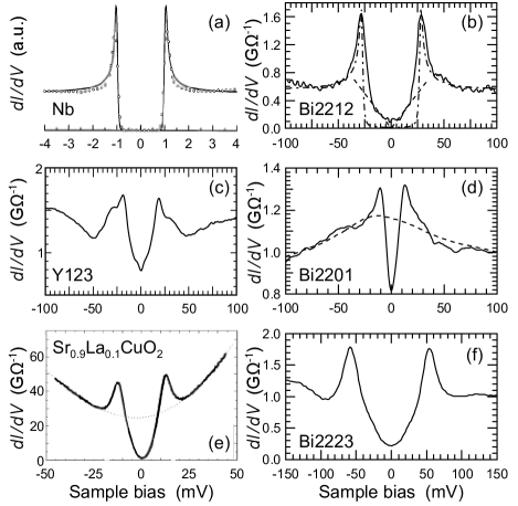
Two of the most striking features of the spectra of Bi2212 are the V-shaped energy dependence near and the very large peaks at the gap edges. The V-shaped low-bias conductance (Fig. 10b) is indicative of nodes in the gap. This is consistent with the -wave symmetry deduced from tricrystal experiments Tsuei and Kirtley (2000) and with the angular dependence observed in ARPES measurements Damascelli et al. (2003); Campuzano et al. (2004). However, this simple model fails to reproduce the large spectral weight in the conductance peaks at the gap edges. Wei et al. (1998a) and Hoogenboom et al. (2003a) showed that both characteristics can be simulated simultaneously by taking into account the band structure, and especially the van Hove singularity (vHs) near the saddle points at and in the Brillouin zone (see Sec. V.2).
The simulated spectral weight in the peaks could also be enhanced by assuming an anisotropic tunneling matrix element, which would filter the tunneling probability in favor of the anti-nodal states near , and suppress the tunneling probability near the nodal states along Yusof et al. (1998); Franz and Tešanović (1999). However, this simple model does not only enhance the DOS in the coherence peaks in agreement with experiment, it also reduces the DOS below the gap too much, producing more -wave looking U-shaped spectra inconsistent with experiments Hoogenboom et al. (2003a).
The tunneling spectra of the three layer Bi-compound Bi2Sr2Ca2Cu3O10+δ (Bi2223) look very similar to those of Bi2212, except that all features are shifted to higher energies (Fig. 10f). On the contrary, the single layer Bi-compound Bi2Sr2CuO6 (Bi2201) yields substantially different spectra (Fig. 10d) with a finite zero-bias conductance and a much larger reduced gap, e.g. in overdoped Bi2201 Kugler et al. (2001). Mashima et al. (2003) measured similar looking spectra on lead-doped Bi2201. The considerable difference between Bi2201 and Bi2212 may stem from the more pronounced two-dimensional nature of Bi2201. Superconductivity in Bi2201 resides in a single CuO2 layer, resulting in larger fluctuations effectively reducing . The much wider temperature range of the pseudogap phase in Bi2201 (see Sec. VI) could be a direct consequence of such fluctuations. The finite zero-bias conductance and the broad peaks at the gap edges remain open issues.
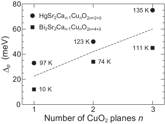
The gap amplitude of hole-doped HTS cuprates series appears to increase with the number of CuO2 planes per unit cell, at least up to for which tunneling data exist. This dependence is depicted in Fig. 11 for two series with very different gap amplitudes: the bismuth series Bi2Sr2Can-1CunO2n+4+δ and the mercury series HgSr2Can-1CunO2n+2+δ. The increase of the gap with in the Bi-compounds is illustrated graphically in Figs. 10d, b, and f showing the tunneling spectra for , 2, and 3, respectively. (Note that the dependence on appears accentuated in Fig. 10 due to the spread of doping levels of that Bi-series.) A similar behavior is observed for : it increases with increasing up to ( decreases upon further increasing ), and can be very different in distinct homogeneous series. Understanding the dependence of the gap and of on the number of CuO2 planes may turn out to be one important key to unravel the mechanism of HTS (see e.g. Pavarini et al., 2001; Chen and Lin, 2004).
V.1.2 Y-compounds
A characteristic SIN spectrum measured on an as grown, fully oxygenated YBa2Cu3O7 (Y123) single crystal ( K) is shown in Fig. 10c. The spectrum reveals a number of remarkable differences compared to Bi2212 with similar : (i) a smaller reduced gap ( in the sample shown here), (ii) a large finite conductance at , and (iii) multiple broad coherence peaks at the gap edges Miller et al. (1993); Maggio-Aprile et al. (1995). The main coherence peaks define a gap of meV, much closer to the value expected for a BCS -wave superconductor than the gap in the Bi-based cuprates discussed above. Additional structures of interest are weak shoulders flanking the main peaks at higher energy, and two weak features often developing below the gap at about meV.
The multiple peak structure does not correspond to the simple -wave expectation. Tachiki et al. (1990) and Miller et al. (1993) ascribed the features inside the gap near meV to weak proximity-induced superconductivity in the BaO and CuO-chain planes. Yeh et al. (2001) identified the peaks at meV and meV with a mixed -wave gap in the CuO2 plane. In this scenario, two sets of conductance peaks are indeed expected, one at and the other at , and being the maximum amplitude of the -wave and -wave component of the gap, respectively. However, this would imply a strong -wave admixture in the Y123 ground state, which is opposed by other experiments, like tricrystal experiments Tsuei and Kirtley (2000), showing a pure -wave. Thus the exact nature of the Y123 ground state and the corresponding interpretation of the tunneling data needs further investigation.
Different ideas have been developed to understand the shoulders outside the main coherence peaks. Such structures have been modeled in terms of the band structure van-Hove singularity Tachiki et al. (1990); Hoogenboom et al. (2003a). Similar, though much weaker, shoulders have been measured on Bi2212 and were ascribed to the onset of a strong coupling effect Zasadzinski et al. (2003). One aspect of Y123, which certainly complicates the analysis of the spectra, is the presence of CuO chains along with the CuO2 planes, and a completely satisfactory description has yet to be devised.
Spectra with a line shape similar to those obtained on Y123 were measured on La1.84Sr0.16CuO4 (LSCO) by Kato et al. (2003). Like Y123, their background conductance is increasing with energy, the DOS at does not vanish, and the reduced gap amounts to . However, unlike Y123, they do not show any multiple peak structure.
V.1.3 Electron-doped HTS
Over the past two decades, some consensus has emerged that the gap symmetry in hole-doped HTS is . In electron-doped HTS, a majority of tunneling experiments point at a more conventional -wave gap, although some do look more consistent with a -wave symmetry. This controversy in electron-doped HTS is illustrated in Nd1.85Ce0.15CuO4-y (NCCO), one of the few electron-doped HTS which has been investigated by STM. Kashiwaya et al. (1998) and Alff et al. (1998) contend that NCCO is an -wave superconductor. Their conclusion is based on the absence of a zero-bias conductance peak (ZBCP) on surfaces perpendicular to the nodal lines (see Sec. V.6), and on the good fit of the spectra obtained with an anisotropic -wave BCS model. A different picture emerges from STM studies by Hayashi et al. (1998b) who conclude that NCCO is a -wave superconductor based on the ZBCP which appears in some of their low-resistance tunnel junction spectra.
Magnetic and non-magnetic impurities provides an indirect probe of the gap symmetry (see Sec. V.5). Non-magnetic impurity scattering has no effect on an -wave superconductor, whereas it will cause pair breaking in a -wave superconductor. Magnetic impurities have the opposite effect and do cause pair breaking in conventional -wave BCS superconductors. The gap measured on Sr0.9La0.1CuO2 (SLCO, Fig. 10e), an infinite layer electron-doped HTS, is in good agreement with an isotropic -wave BCS model Yeh et al. (2002). Yeh et al. report that doping SLCO with nickel, a magnetic impurity, has a large effect on the line shape of the LSCO spectra, whereas doping with Zn, a non-magnetic impurity, has very little effect as expected for an -wave superconductor. In Bi2212, a -wave hole-doped HTS, the opposite seems to happen, where zinc doping is most detrimental to superconductivity Hudson et al. (2001)—Note that in both compounds, the impurity atom is substituting for the copper atom in the CuO2 plane. Such studies of atomic scale impurities in HTS are discussed further in Sec. V.5.
V.2 Dip-hump structure
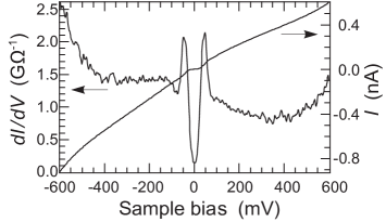
Sec. V.1 was devoted to the region of the tunneling conductance curves below the superconducting gap. Here, we extend the discussion to include the conductance background at higher energy beyond the gap. Figure 12 shows a typical large energy range spectrum of Bi2212 exhibiting a sizeable electron-hole asymmetry in the background conductance (see also Sugita et al., 2000). A very similar background was measured on Bi2223 Kugler et al. (2006). The increasing conductance at high energy beyond meV may be a signature of the valence bands below .
A remarkable dip structure develops outside the superconducting gap on top of a smooth broad maximum in the background conductance near . In early STM experiments, this dip was mostly obscured by an increasing (linear or parabolic) background conductance (e.g. Liu et al., 1994). The dip became clearly apparent in spectra obtained with the best STM junctions, as defined in Sec. IV.3. In Bi2212, the dip is systematically seen at negative sample bias Renner and Fischer (1994a, 1995). A symmetric dip is present at positive bias in some exceptional cases DeWilde et al. (1998); Hudson et al. (1999). The dip structure, often accompanied by a hump at higher energy, is at the core of a heated debate. One key question is whether it is a band structure or a strong coupling effect.
Band-structure effects would be a natural possibility to explain the dip. ARPES spectra, which first showed the same dip feature beyond the gap Dessau et al. (1991); Hwu et al. (1991), have been interpreted along those lines. However, this interpretation is not widely accepted. Zasadzinski et al. (2003) exclude in particular the possibility that the dip is due to a vHs or that it results from the superconducting gap opening in a pseudogap background.
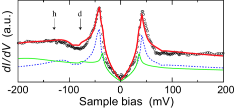
Strong coupling effects are another possibility to explain the dip. They are known to have similar effects on tunneling spectra in conventional superconductors. Tunnel junctions on lead, for example, reveal some fine structure in the differential conductance above the gap, which was shown to correspond to peaks in the phonon density of states . The fine structure was directly linked to the electron-phonon mechanism of superconductivity, and the electron-phonon spectral function could be quantitatively obtained through inversion of the spectra using strong coupling Eliashberg theory Schrieffer et al. (1963); McMillan and Rowell (1965). This eventuality has been addressed by Zasadzinski et al. (2003) to fit a particular symmetric Bi2212 spectrum normalized to an arbitrary state-conserving normal-state background. Using a modified Eliashberg model to account for the -wave symmetry, Zasadzinski et al. (2003) self consistently reproduce the overall shape, position and magnitude of the dip as well as the superconducting gap structure with a single narrow bosonic mode centered at meV.
In the strong coupling scenario, the dip could be due to a phonon mode (as in low-temperature superconductors) or to a collective electronic mode. A candidate electronic mode was observed by neutron scattering near at meV in Y123 Fong et al. (1995), and subsequently in Bi2212 Fong et al. (1999). This mode was determined to scale with He et al. (2001), suggesting a close relation with the superconducting state. Specific models were developed to describe the coupling of the electrons to this mode Eschrig and Norman (2000). Hoogenboom et al. (2003b) used this model to calculate the spectra of Bi2212 using doping-dependent band structure parameters from ARPES, including the bilayer splitting, and the electronic mode measured by neutrons. The result is plotted as the red curve in Fig. 13. Note the importance of the bilayer splitting to obtain the proper background conductance intensity relative to the peaks height. In this model the asymmetry of the dip with respect to is not a consequence of the nature of the mode (e.g. phonon or spin wave) but is due to the presence of the vHs at negative energy.
V.3 Doping dependence of the superconducting gap
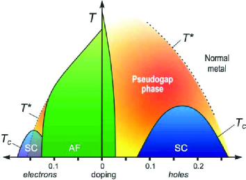
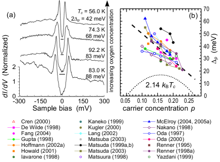
A generic doping phase diagram of HTS is shown in Fig. 14. Undoped cuprates are antiferromagnetic (AF) Mott insulators with one electron per copper site in the CuO2 plane. Upon adding either holes or electrons, they eventually become superconducting (SC) and increases to reach a maximum at optimal doping before vanishing again at higher hole or electron concentration.
A series of unusual properties characterize hole-doped cuprates, including a pseudogap, non Fermi liquid behavior, and an unusual superconducting state. These properties depend on doping, and are most anomalous in underdoped compounds (i.e. at doping below optimal).
In conventional BCS superconductors, is proportional to the superconducting transition temperature , and the reduced gap lies in the range to . A surprising result was that for most HTS compounds, STM tunneling spectroscopy and related methods (planar, break, and point-contact tunnel junctions) as well as ARPES spectroscopy, found a very large and doping-dependent reduced gap (Fig. 15). This result reflects the absence of scaling of the superconducting gap with (Fig. 15b). In overdoped Bi2212, the gap decreases with decreasing , as expected. But in underdoped Bi2212, the gap increases with decreasing Renner et al. (1998a); Miyakawa et al. (1999). The reduced gap defined in the standard way ranges from 4.3 to values as high as 28 Kugler et al. (2001). This wide range suggests that , the temperature where phase coherence and a macroscopic superconducting state are established, is not the appropriate energy scale to describe the gap. Replacing by , the temperature where the pseudogap appears, enables to recover a constant reduced gap with a more conventional value close to Kugler et al. (2001); Dipasupil et al. (2002); Nakano et al. (2003) expected for a -wave BCS superconductor (see Sec. VI). Other spectroscopic features also show a characteristic doping dependence in Bi2212. The dip-hump feature discussed in Sec. V.2 becomes weaker and shifts closer to the coherence peaks in underdoped and overdoped compounds Zasadzinski et al. (2001). The background conductance shows a systematic evolution, becoming gradually more asymmetric with decreasing hole concentration (Fig. 15a). Likewise, the coherence peaks are most asymmetric in highly underdoped crystals Miyakawa et al. (1999). The change in the background conductance can be partly explained in terms of the vHs shifting away from in underdoped Bi2212 Hoogenboom et al. (2003a). However, the more pronounced asymmetry observed in heavily underdoped samples has been ascribed to strong-correlations effects Rantner and Wen (2000); Anderson and Ong (2006). The smeared coherence peaks at the gap edges in underdoped Bi2212 may be a consequence of the very short quasiparticle lifetime due to the proximity of a Mott insulator.
The doping dependence of the gap of Y123 is much less documented than Bi2212. Deutscher (1999) and Yeh et al. (2001) report that unlike in Bi2212, the gap in Y123 does scale with as a function of doping, and the reduced gap does not reach as high values as in Bi2212. remains much closer to conventional superconductors, ranging from 7.8 (underdoped) to 4.5 (overdoped). Kohen et al. (2000) and Yeh et al. (2001) report another interesting observation in Y123, namely that the symmetry of the gap is changing from pure -wave to -wave or -wave above optimal doping (see discussion in Sec. V.1.2). Vobornik et al. (1999) claimed to observe a similar crossover from a -wave to a less anisotropic gap in overdoped Bi2212 in ARPES experiments. However, this result is in contradiction with STM spectroscopy, which shows the same linear energy dependence of the conductance near throughout the entire superconducting range Renner et al. (1998a); Miyakawa et al. (1999).
V.4 Spatial gap (in-)homogeneity
The question of spatial homogeneity of the superconducting gap has stirred up a lot of interest. This ongoing excitement is driven by models where electronic phase separation is at the core of the high superconducting transition temperature Phillips et al. (2003). Two types of spatial inhomogeneities of the local DOS emerge from STS studies of Bi2212: (i) spatial inhomogeneity of the superconducting gap amplitude, and (ii) spatial inhomogeneity of the low-energy DOS, deep inside the gap. The latter is seen as a periodic electronic modulation, where is the unit-cell lattice parameter Howald et al. (2003a); Hoffman et al. (2002a). Recently, a similar electronically modulated phase was also found to develop in the pseudogap state of Bi2212 above Vershinin et al. (2004a) as well as in superconducting and non-superconducting Ca2-xNaxCuO2Cl2 Hanaguri et al. (2004). These DOS modulations appear intimately linked to the HTS state, and are the focus of Sec. VIII. Here, we shall discuss the notorious spatial inhomogeneities of the gap amplitude observed in Bi2212.
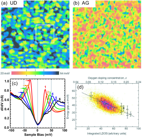
Inhomogeneous superconductivity in Bi2212 was reported in a number of STM studies Cren et al. (2000); Howald et al. (2001); Pan et al. (2001); Lang et al. (2002); Kinoda et al. (2003). Real-space STS maps of the local superconducting gap shown in Figs. 16a,b reveal a network of nanometer-scale islands, on average – nm wide, with different gap amplitudes.111111Degraded or contaminated surfaces also lead to spatial variations of the tunneling spectra, but of a very different kind (see Sec. VI.2.2).
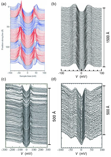
The key question is to what extent this inhomogeneity is an intrinsic phenomenon at the core of high temperature superconductivity? By intrinsic we mean an electronic effect, possibly related to the mechanism for HTS, taking place in an otherwise homogeneous system. Electronic phase separation would be one candidate phenomenon Phillips et al. (2003). This is in contrast to an extrinsic origin of the spectral inhomogeneities, by which we mean a phenomenon unrelated to HTS, resulting from stoichiometric inhomogeneities such as the distribution of atoms and dopants. Howald et al. (2001) argued strongly in favor of an intrinsic inhomogeneity. They pointed out that the boundaries between the domains are always of the order of the coherence length and that there was no obvious correlation with structural inhomogeneities of the sample. Their conclusion was that this disorder represents a phase separation phenomenon into “good and bad superconducting regions”. Such an interpretation has also been put forward by Pan et al. (2001) and Lang et al. (2002). On the contrary, Renner and Fischer (1994b) noted the existence of such inhomogeneities and concluded that they are related to chemical inhomogeneities. They further found that homogeneous tunneling spectra can be obtained, and they demonstrated atomic resolution under these conditions Renner and Fischer (1995). Hoogenboom et al. (2003b) showed that homogeneous samples could be obtained by adequate annealing, at least in the overdoped case. They concluded that inhomogeneity is most likely due to inhomogeneous oxygen distribution and that it is not an essential part of the mechanism for HTS. Thus, in recent years, there has been a controversy about the interpretation of these inhomogeneities. Although this question is not definitively settled, the authors of this review are of the opinion that there is more and more experimental evidence for the extrinsic scenario. In the following, we shall develop further arguments on which this statement is based.
The first piece of evidence comes from a series of experiments showing reproducible spectra with very little spread in gap amplitude in Bi2212, Bi2223, Y123 (Fig. 17b–d) and NdBa2Cu3O7-δ Nishiyama et al. (2002) single crystals. These measurements were made in conditions where concurrent atomic resolution and/or STS vortex-core imaging could be achieved, indicating that, if present, changes in the spectral signature, even over sub-nanometer distances, could be detected. Such distances are much shorter than the typical size of the domains seen in inhomogeneous samples (Figs. 16a,b), and the observed homogeneity can not be ascribed to a broad STM tip.
A second piece of evidence showing that inhomogeneous superconductivity is not essential for a high comes from STM studies by Matsuba et al. (2003b). They observe that the spread in gap amplitude can be very different in distinct regions on a given Bi2212 surface, although the average gap value, and possibly , are the same. In another systematic study of slightly overdoped Bi2212, Hoogenboom et al. (2003b) demonstrated that spatial gap inhomogeneities as shown in Figs. 16a,b and 17a were intimately associated with a broad superconducting transition, as measured by ac-susceptibility on the same samples. Conversely, single crystals with narrow superconducting transitions ( K) yield very homogeneous tunneling spectroscopy as shown in Fig. 17b. This correlation between a wide gap distribution and the ac-susceptibility transition width was also observed in Bi2223 Kugler et al. (2006), and suggests that the nanometer length scale gap inhomogeneities stem from extrinsic stoichiometric disorder rather than intrinsic electronic phase separation.
A very recent study provides further compelling experimental evidence that the gap inhomogeneity is indeed an extrinsic stoichiometric effect, as inferred from the above experiments. Combining high resolution topographic and spectroscopic STM maps, McElroy et al. (2005b) captured the direct correlation between the gap amplitude and oxygen impurity distributions in real space. This result is in agreement with the spread of spectra measured on inhomogeneous samples McElroy et al. (2005a), whose line shapes vary from typical for optimally-doped samples (Fig. 16c, spectrum 1) to typical for heavily underdoped samples (Fig. 16c, spectrum 6). Note however that the detailed relation between the local gap and the local oxygen impurity distribution remains unclear and requires further investigations.
In summary, the spatial inhomogeneities in the gap amplitude appear to be driven by a property which transition metal perovskite oxides share with all oxides, namely their propensity to high concentration of defects, especially oxygen inhomogeneities. Note that lead impurities and disorder in the Sr and Ca layers were found to have no effect on the gap inhomogeneity Kinoda et al. (2003). These results all point at oxygen disorder as the main cause for the inhomogeneities found by spectroscopy. Generally, as-grown samples tend to be inhomogeneous and this tendency increases as doping is reduced. However, these inhomogeneities are not consistent with simple charge segregation in a perfect lattice. Special post-synthesis treatments allow to make more homogeneous samples with equally high , as has been clearly demonstrated in overdoped Bi2212 Hoogenboom et al. (2003b). Most importantly, the experimental evidence is that an inhomogeneous gap distribution is not a prerequisite to the occurrence of high temperature superconductivity, since there is no correlation between such a distribution and the value of . However, note that the oxygen concentration and distribution are probably not the only differences between samples from different sources and batches. Therefore in a detailed comparison between samples other parameters have to be taken into account as well.
V.5 STM on impurities
Impurities in superconductors have been a subject of research since the BCS theory was established. Whereas non-magnetic impurities were found to have little or no effect on , magnetic impurities turned out to suppress superconductivity. Indeed, for -wave superconductors the Anderson theorem Anderson (1959) states that non-magnetic impurity scattering does not reduce , whereas Abrikosov and Gor’kov (1960) showed how magnetic impurities reduce to zero through exchange scattering at impurity concentrations of the order of one percent. Later on Yu (1965), Shiba (1968), and Rusinov (1969) independently found that a magnetic impurity can induce quasiparticle sub-gap bound states. The first direct observation of such behavior by STM was reported by Yazdani et al. (1997) on a Nb surface with Mn, Gd or Ag adatoms. Ag, believed to be non-magnetic, has no effect on the superconducting -wave state. However when Mn or Gd are deposited on the surface of Nb the zero-bias conductance is enhanced when tunneling through magnetic Mn and Gd. The spatial extension of the impurity effect is about 10 Å and the resulting spectra were found to be asymmetric.
In a -wave superconductor Anderson’s theorem does not hold and it is expected that non-magnetic impurities have a profound effect on the superconducting properties. This has been investigated by several groups Lee (1993); Byers et al. (1993); Balatsky et al. (1995). These theories predict local signatures of -wave pairing, and variations in the LDOS around the impurities. A review of these theories has been given by Balatsky et al. (2006).
First attempts to study impurities in HTS by STM were carried out by Yazdani et al. (1999) and by Hudson et al. (1999). The former studied Bi2212 surfaces onto which nanoscale Au dots were deposited from the STM gold tip. It was found that strong zero-bias enhancements occurred in when the tip was placed just above these particles, demonstrating the existence of a strong resonance as expected for a -wave superconductor. In the latter paper an undoped Bi2212 crystal was studied. Their approach was to make zero-bias conductance maps similar to Yazdani et al.. These maps showed nanoscale areas with an unusually high zero-bias conductance. Analyzing these unveiled a zero-bias anomaly corresponding to what would be expected from scattering of a -wave superconductor on an impurity. However, the nature of these impurities was not identified in this work.
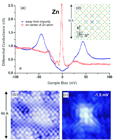
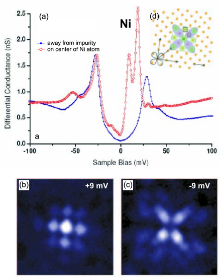
Following this Pan et al. (2000b) investigated Zn-doped Bi2212. They found an intense quasiparticle scattering resonance at meV at many sites on the surface of the sample. Since Zn substitutes for Cu, two layers below the surface, it is not seen in topography. However the effect of the resonant scattering can be seen at low energies. The density of such sites corresponds to about one third of the nominal concentration of Zn atoms and it is therefore reasonable to assume that the strong zero-bias sites reflect the effect of Zn doping. Fig. 18a shows the spectra away from the impurity and on top of it, the latter displaying a strong zero bias anomaly coincident with a strong suppression of superconductivity within a 15 Å radius of the scattering sites. Imaging of the spatial dependence of the quasiparticle density of states in the vicinity of the impurity atoms directly reveals the four-fold symmetric quasiparticle ‘cloud’ aligned with the nodes of the -wave superconducting gap (Figs. 18b–d). Whether this structure reflects the symmetry of the superconducting state or the symmetry of the atomic lattice remains to be determined.
Particularly interesting in this context is the comparison of the effects of magnetic and non-magnetic impurities substituted on equivalent Cu sites. In comparison to Zn impurities, magnetic Ni impurities lead to a very different behavior. This was studied by Hudson et al. (2001). At each Ni site they observe two -wave impurity states of apparently opposite spin polarization, whose existence indicates that Ni retains a magnetic moment in the superconducting state (Fig. 19a). However, analysis of the impurity-state energies shows that quasiparticle scattering at Ni is predominantly non-magnetic. The spatial distribution of the conductance maxima around the impurity is strongly asymmetric with respect to the Fermi level (Figs. 19b and c). Furthermore, they show that the superconducting energy gap is unimpaired at Ni. This is in strong contrast to the effects of non-magnetic Zn impurities, which locally destroy superconductivity.
Motivated by the STM observations, several microscopic calculations of the electronic structure near Zn or Ni impurities have been reported. Most of these calculations are based on the BCS -wave theory, and they differ mainly by the model employed for the impurity, and the treatment of the superconducting order parameter modification around the impurity site. In short, impurity potentials in a BCS -wave state induce resonances, either below or above the Fermi energy depending upon the sign of the potential. In the unitary limit the resonance approaches the Fermi energy. The measured LDOS around Zn impurities, however, turns out to be more difficult to understand in this class of models. Indeed for strong point-like impurities the spectral weight is expelled from the impurity to the neighboring sites, and the LDOS at the impurity site is nearly zero, in contrast to experiment. Various solutions to this problem have been put forward. Zhu et al. (2000), Zhu and Ting (2001a), and Martin et al. (2002) invoked an anisotropic tunneling matrix element, which would filter the tunnel electrons in such a way that the current measured on top of the impurity site in effect originates from the neighboring sites. Other authors claimed that correlation effects and the formation of a local moment at the Zn site are important Polkovnikov et al. (2001). Recently Tang and Flatté (2004) were able to give a fairly complete account of the experimental Zn impurity LDOS by assuming that the Zn potential has a finite spatial extension, and by including a modification of the pairing potential and hopping energies in the neighborhood of the Zn site. Which one of these interpretations of the STM data is the right one is still unclear.
V.6 Cross-sectional tunneling
Most published STM experiments were carried out with the STM tip positioned perpendicular to the perovskite surface. In this -axis tunneling configuration, tunneling samples an angular average over the -plane density of states (see Sec. III). Here, we briefly review the few attempts to do cross-sectional tunneling, i.e. tunneling into an arbitrary plane parallel to the direction with the STM tip perpendicular to the direction. This geometry is attractive for several reasons. It should enable a direct probe of the alternate stacking of insulating and superconducting layers along . It further should allow to probe the symmetry of the gap in the CuO2 sheets by measuring the gap amplitude as a function of the surface orientation and by detecting the zero-bias conductance peak (ZBCP) expected on and surfaces.121212The main theoretical expectations for the electronic structure of superconductors near surfaces or interfaces have been reviewed by Löfwander et al. (2001) and Deutscher (2005).
Cross-sectional tunneling is a very challenging endeavor, primarily due to the difficulty in preparing a suitable surface for STM. The first experiments were performed on Bi2212, resulting in topographic images with atomic scale resolution of the surface Hasegawa and Kitazawa (1990); Hasegawa et al. (1991b). Hasegawa et al. also found spectroscopic signatures of the alternate stacking along of gapped BiO layers and metallic CuO2 layers.
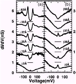
The potential to gather experimental evidence of the symmetry of the superconducting gap has compelled several groups to attempt cross-sectional tunneling experiments. Suzuki et al. (1999c) cut thin Bi2212 single crystals along different planes and probed the exposed surfaces by STM. The surface revealed a conductance peak at . All other surfaces were gapped, with the largest gap on the surface. This is precisely what is expected for a gap in the plane. Kane and Ng (1996) did a similar experiment, tunneling into edges of a Bi2212 single crystal using a wire aligned parallel to the -axis as the “tip” electrode. These experiments yield a very different result: all surfaces show a gapped spectrum (no ZBCP), and the largest gap is measured on surfaces. This angular dependence of the gap is suggesting symmetry. However, the absence of any ZBCP makes this experiment inconclusive.
Misra et al. (2002b) circumvent the difficulty of preparing cross-sectional surfaces by measuring tunneling characteristics along a oriented step edge of a Bi2212 thin film. The step should give rise to a ZBCP in a superconductor with a gap in the plane Hu (1994). Indeed, they do find a clear signature of a conductance peak at in the vicinity of the step (Fig. 20). Another interesting result reported by Misra et al. (2002b) is the absence of a ZBCP near a twin boundary in Bi2212, indicating that such crystallographic defects are not a strong perturbation for the superconducting state—unlike in Y123, where STM measurements in a magnetic field show that they strongly perturb the superconducting condensate Maggio-Aprile et al. (1997).
In Y123, Yeh et al. (2001) were able to measure the ZBCP as a function of position along the surface of an optimally-doped single crystal (Fig. 21a). The same experiment along the surface showed a large gap at , in agreement with symmetry. Y123 can be grown as oriented thin films, thus offering an alternative approach to measuring the ZBCP. Yeh et al. (2001) measured the expected ZBCP on such films, but could not achieve atomic-resolution imaging. Conversely, Nantoh et al. (1995) achieved atomic-resolution imaging of oriented thin films, but failed to observe a ZBCP.
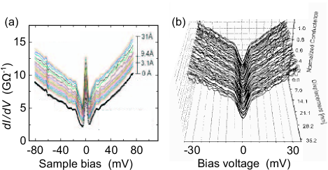
Tanaka et al. (1995) measured spatially homogeneous and tip-to-sample distance independent tunneling spectra on the surface of La1.85Sr0.15CuO4 (La214). However, the spectra show a ZBCP, which is not consistent with symmetry, but indicates symmetry. Tanaka et al. (1994) also found a gap by cross-sectional spectroscopy in Y123. Introducing momentum-dependent tunneling currents to take the shape of the electron wave function of the surface oxygen atoms into account for the evaluation of the tunneling matrix elements, Tanaka et al. (1995) argue they can reconcile their data with a symmetry of the gap.
The ZBCP appears to be a characteristic property of and surfaces of hole-doped HTS, in agreement with the -wave symmetry of the gap. Most STM experiments favor -wave superconductivity in electron-doped HTS. One argument is the absence of a ZBCP on surfaces Kashiwaya et al. (1998); Alff et al. (1998) as shown for Nd1.85Ce0.15CuO4-y (NCCO) in Fig. 21b. Hayashi et al. (1998b) measure a ZBCP on the surface of NCCO, suggesting a symmetry. However, this result seems less systematic, as the ZBCP is only observed in some of their low-resistance junctions. The relation of these results to other experiments showing -wave symmetry needs further clarification.
The ZBCP has been more extensively investigated using planar and point contact tunnel junctions, including the influence of disorder and magnetic field (see e.g. Aprili et al., 1998, 1999). A very comprehensive discussion of probing the ZBCP by tunneling can be found in two recent reviews by Kashiwaya and Tanaka (2000) and Deutscher (2005).
V.7 Summary
The very unusual nature of tunneling spectra measured on HTS was recognized from the first successful tunneling experiments, and caught immediate attention. Most striking were the unconventional line shape in hole-doped cuprates, with a finite density of states in the gap, and the large energy scale of the characteristic spectral features. The low-energy line shape has since been explained in terms of the -wave symmetry of the gap. Higher-energy spectral features above the gap are still matter of discussion—although some very good theoretical fits have been worked out—in particular the asymmetric and doping dependent background and dip-hump.
The energy scale of the gap feature in HTS is way off the expectations of the conventional theory for superconductivity. This is in particular the case for the bismuth compounds (Bi2201, Bi2212, Bi2223). In these materials the gap depends on the doping and number of CuO2 planes in the unit cell, and grows with reducing hole concentration and increasing number of planes. This leads in certain cases to exceptionally high values of . This surprising behavior has to be viewed in relation to the properties of the pseudogap, to be discussed in the next section.
Spatial inhomogeneities of the superconducting gap have stirred up considerable interest, fuelled in part by models where phase separation plays a key role for high-temperature superconductivity. However, experimental evidence strongly suggests that such inhomogeneities are an extrinsic effect, stemming from stoichiometric variations. Most importantly, they are correlated with the superconducting transition width, but not with the maximum value of the bulk transition temperature. Magnetic and non-magnetic atomic impurities intentionally introduced into the CuO2 planes result in a particular kind of local inhomogeneity, providing an original local test of the pairing state.
VI The pseudogap
Many experimental techniques provided evidence for an unconventional normal state common to all HTS and characterized by the opening of a gap in the electronic excitation spectrum at a temperature above the critical temperature , the so-called ‘pseudogap’ (PG). This observation initiated an intense debate about its origin, since the answer to this question may turn out to be essential for the understanding of high- superconductivity (for a review see Timusk and Statt, 1999).
The various theoretical interpretations of the pseudogap phenomenon may be roughly classified in two groups: (i) The pseudogap is the manifestation of some order, static or fluctuating, generally of magnetic origin, but unrelated to and/or in competition with the superconducting order.131313Most of these theories view the superconducting state of the cuprates as a consequence of doping a Mott insulator. Lee et al. (2004) give a comprehensive review of this type of approach. In the resonating valence bond (RVB) theory Anderson (1987) argued that the ground state of a doped antiferromagnet would be a liquid of singlet spin pairs. In this framework the pseudogap appears as the spin gap associated with the breaking of the RVB singlets Paramekanti et al. (2001); Anderson et al. (2004). Several authors have considered the possibility that doping the cuprates has the effect of weakening some order present in the parent compound. The pseudogap would thus be a consequence of this order which progressively disappears upon doping as superconductivity sets in, and would vanish at a quantum critical point (QCP) presumably below the superconducting dome. This (possibly dynamical) order could be the AFM order itself Kampf and Schrieffer (1990), a state of microscopic orbital currents known as staggered-flux state Affleck and Marston (1988) or -density wave (DDW) state Schulz (1989); Wen and Lee (1996); Varma (1997); Chakravarty et al. (2001), a stripe state in which the doped holes order into one-dimensional patterns (Zaanen and Gunnarsson (1989); Emery et al. (1990); White and Scalapino (1998); the field was recently reviewed by Kivelson et al. (2003) and Carlson et al. (2004)), a spin-density wave (SDW) and/or charge-density wave (CDW) state Chubukov et al. (1996); Varlamov et al. (1997); Vojta and Sachdev (1999). In some of these theories the two orders appear as two faces of the same coin Zhang (1997), or they turn out to be dual one to another Franz and Tešanović (2001); Wang (2004). (ii) The pseudogap is the precursor of the superconducting gap, and reflects pair fluctuations above .141414The short coherence length of the cuprate superconductors suggests that they lie somewhere between the BCS limit of very large momentum-space pairs and the opposite case of small real-space pairs undergoing a Bose-Einstein condensation (BEC) (see the review of Chen et al., 2005). In this picture the pseudogap is the binding energy of the preformed pairs above Geshkenbein et al. (1997). The BCS-BEC crossover scenario has been studied within the boson-fermion model Ranninger et al. (1995) and attractive Hubbard model Moreo et al. (1992); Randeria et al. (1992); Micnas et al. (1995). Other approaches emphasize the weak phase stiffness in the underdoped cuprates resulting from the low superfluid density, which would lead to a suppression of by phase fluctuations Emery and Kivelson (1995); Schmalian et al. (1997); Franz and Millis (1998); Giovannini and Berthod (2001); Eckl et al. (2002); Lammert and Rokhsar (2001). At present, a definitive answer is still lacking, although the STS results favor the latter, as we shall see, or more generally a situation where both phenomena have the same origin.
Closely related to this fundamental issue is the understanding of the HTS doping phase diagram, schematically shown in Fig. 14. How does the pseudogap vary with doping, temperature, and magnetic field? How does the pseudogap scale with and the superconducting gap? Is there a universal HTS doping phase diagram?
In this section we review the key STS results related to the pseudogap under different experimental conditions. In Sec. VI.1 we describe the -dependence of the LDOS of Bi2212, Bi2201, and Y123 and we analyze the scaling relations between the pseudogap and the superconducting gap. In Sec. VI.2 we address the observation of the pseudogap at low temperatures inside vortex cores and on disordered surfaces. In Sec. VI.3 we discuss the doping phase diagram which results from the tunneling experiments reviewed here and finally, in Sec. VI.4, we highlight the key results of this section. The connection between the pseudogap and the recently reported experiments revealing spatial modulations in the LDOS are discussed separately in Sec. VIII.
VI.1 Temperature dependence of the local DOS
Already by the end of the eighties bulk techniques revealed an unconventional normal state behavior above , but it took about a decade to obtain sufficient sample and surface quality to evidence the PG spectral signature directly in the DOS using ARPES Ding et al. (1996); Loeser et al. (1996) and STS Renner et al. (1998a).
Measuring the -dependence of the LDOS by STM is a challenge. The difficulty is to avoid the tip from shifting relative to the sample when the temperature is changed, due to uncompensated thermal expansion coefficients in the experimental setup. If the tip does shift, as is usually the case, variations in the characteristics may not only be due to temperature, but also to the different tunneling locations, especially if the spectroscopic properties are not homogeneous over sufficiently large areas as discussed in Sec. V. Not surprisingly, there are only few relevant -dependent STM studies of HTS. The first successful STM experiments where obtained on Bi2212 Renner et al. (1998a); Matsuda et al. (1999b), followed by Y123 Maggio-Aprile et al. (2000) and Bi2201 Kugler et al. (2001).
VI.1.1 The case of Bi2212
Historically, the first tunneling results revealing the pseudogap (PG) were reported on Bi2212 by Tao et al. (1997) on planar junctions and by Renner et al. (1998a) using an STM junction. These experiments showed unambiguously that HTS do not follow what the BCS theory predicts, namely that the superconducting gap closes at . In this theory, indeed, both the pairing and the phase coherence are lost simultaneously at . The origin of this behavior is illustrated by the reduced gap value for an -wave BCS superconductor, telling that at the mean field critical temperature , thermal fluctuations are strong enough to overcome the pairing energy . In the case of UD Bi2212, reduced gap values as high as 20 have been reported Miyakawa et al. (1999), providing a strong hint that the -dependence of the superconducting gap of HTS might be very different from the BCS mean-field behavior.
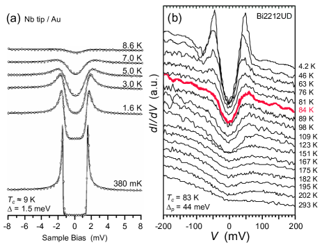
Figure 22 illustrates the -dependence of the quasiparticle DOS of Niobium Pan et al. (1998a),151515Note the different gap amplitude compared to Fig. 10a for the same experimental configuration, which Pan et al. (1998a) tentatively ascribe to the detailed geometry, structure, and composition of the Nb tip apex. a conventional BCS superconductor, and of UD Bi2212 Renner et al. (1998a). The most striking difference with Nb is the existence in Bi2212 of a clear pseudogap at . The pseudogap has basically the same amplitude as the superconducting gap. Both appear to be essentially -independent, seemingly filling up rather than closing with increasing temperature Tao et al. (1997) except for a slight tendency of the pseudogap to increase upon approaching (see Fig. 26). We point out that, although it is well known that in Nb the gap is closing, this is not obvious when looking at Fig. 22a. The superconducting gap of Nb is of the order of 1.5 meV and K. Thermal smearing therefore prevents to follow the coherence peaks in the DOS up to . In contrast, in the case of UD Bi2212 shown in Fig. 22b, the gap magnitude is about 44 meV for K. Hence and thermal smearing effects relative to are much weaker. If the -dependence of the gap would be BCS-like, one should thus clearly see it in Fig. 22b. This is not the case.
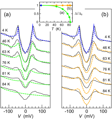
The observation that in Bi2212 the gap magnitude is to first approximation -independent rather than following a BCS-like dependence is highlighted in Fig. 23. Here, the 4.2 K data of Fig. 22b is fitted by a -wave BCS DOS (blue curve). The asymmetric background is generated by pushing the van Hove singularity of the tight-binding dispersion down to meV. Subsequently, the spectrum is recalculated at each temperature corresponding to the experimental data of Fig. 22b up to by assuming two different -dependencies for the gap: (i) a BCS -wave -dependence which simulates a closing gap (Fig. 23a); (ii) a -independent gap (Fig. 23b). This latter simulation reproduces much better the -behavior of the gap magnitude than the BCS case. Looking more carefully to the data (Fig. 22b) reveals other key features which are generic for the -dependence of the DOS in Bi2212.
First, by rising the temperature, the coherence-peak intensity is rapidly reduced at the bulk . The coherence peak at negative bias, as well as the dip-hump feature, are suppressed and a reduced peak shifting to a slightly higher energy remains at positive bias. The suppression of the coherence peaks at clearly observed in Figs. 22b, 24a, and 25a, is a strong evidence that in Bi2212, at the surface is identical to the one of the bulk.161616This is true under the assumption that the coherence peaks are indeed due to superconductivity. This fact is generally accepted and has furthermore been demonstrated in detail by ARPES Feng et al. (2000). We note however that in some cases, and predominantly on underdoped samples which are more prone to inhomogeneous oxygen distributions (see Sec. V), the observation of this typical PG signature does not always coincide with the bulk Matsuda et al. (1999b, a). As mentioned earlier, a possible explanation could be that, due to thermal drift and sample inhomogeneity, the tip probes regions with different doping levels as the temperature is changed. Conversely, a -independent gap magnitude, as observed in Fig. 22b, proves a high level of homogeneity and it demonstrates that the local doping level is not changing with temperature. This point is reinforced by the finding that the asymmetric background conductance is not changing with temperature (Fig. 22b). The argument is based on the observation that the slope of the background is varying with doping Kugler et al. (2006), possibly as a consequence of band-structure effects Hoogenboom et al. (2003a) and/or strong-correlation effects Rantner and Wen (2000); Anderson and Ong (2006). For a discussion of the background conductance, see also Sec. V.3.
Second, crossing , the superconducting spectra evolve continuously into the pseudogap with a gap magnitude which is to first approximation constant. It is clear from Figs. 22b and 24 that the pseudogap also does not change much with temperature except by a general broadening of the gap edges due to thermal smearing at high temperatures. The pseudogap is thus filling up—hence the zero-bias conductance increases monotonically with temperature as reported first by Tao et al. (1997)—and smoothly vanishes at a crossover temperature , which appears to be about room temperature in the data shown in Fig. 22 on UD Bi2212 (see Table 2).
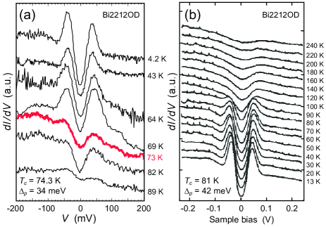
A third remarkable property is illustrated in Fig. 24: The pseudogap is not only bound to the underdoped regime, but also exists in overdoped samples Renner et al. (1998a); Matsuda et al. (1999b, a). The main difference with the underdoped case is that the gap and pseudogap magnitudes are smaller and that the pseudogap seems to vanish more quickly with increasing temperature. Indeed, the PG temperature for UD Bi2212 is about room temperature (Figs. 22b and 25a). In overdoped samples, with correspondingly smaller gaps, is smaller but well above (Fig. 24a). These results indicate that the PG magnitude and the PG temperature are scaling with the superconducting gap in Bi2212. This key observation is discussed in Sec. VI.1.5.
Recently Vershinin et al. (2004a, b) succeeded in studying the spatial dependence of the tunneling conductance in the PG state above on Bi2212. They observed spectra consistent with the generic PG signature described above. Investigating conductance maps at low energies, they also found small variations in the LDOS with an energy-independent incommensurate periodicity. The origin of these modulations and their connection to the PG state are discussed in Sec. VIII.
STM junctions are generally of the SIN type, whereas techniques like point-contact break-junction tunneling (PC-BJT) and intrinsic Josephson junction tunneling (IJJT) provide SIS tunneling barriers. In the following we briefly comment on the main findings of those techniques and compare them to STM vacuum tunneling.
In the case of PC-BJT, a tip is driven into the sample surface. By slightly reducing the pressure applied by the crashed tip it is possible to pick up a cleaved crystal piece, thus providing a SIS vacuum tunnel junction with typical tunnel resistances of 10–100 k Ozyuzer et al. (2000); Dipasupil et al. (2002). In the case of IJJT, the Bi-based cuprate crystal is considered as a stack of multiple Josephson junctions formed between the superconducting CuO2 planes separated by insulating BiO layers. Driving a current along the -axis of small crystal mesas provides intrinsic SIS junctions without any vacuum barrier and with typical tunnel resistances below 10 per junction Kleiner et al. (1992); Suzuki et al. (1999c); Yurgens et al. (1999); Krasnov et al. (2000).
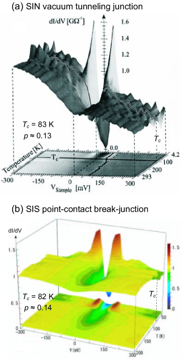
In Fig. 25 we show results reported by Dipasupil et al. (2002) on Bi2212 SIS junctions using PC-BJT and compare them to the STM data by Renner et al. (1998a) on a Bi2212 SIN junction. The spectral features at low temperatures, like the dip-hump and the characteristic -wave V-shaped DOS, as well as the overall -dependence, including the observation of the pseudogap on overdoped samples, and the scaling behavior between and , are remarkably consistent. However, various studies by other groups showed that strong discrepancies exist among data acquired with the PC-BJT technique: data reported by Miyakawa et al. (1998) did not show any pseudogap on optimally-doped Bi2212 and results by Ozyuzer et al. (2002) on underdoped Bi2212 with K showed PG-like spectra that vanish already at about 80 K. The origin of these diverging results is most likely due to the ill-defined junction geometry and to the difficult junction control under variable temperatures.
Over the past years IJJT in Bi2212 Suzuki et al. (1999c); Krasnov et al. (2000); Heim et al. (2002) and Bi2201 Yurgens et al. (2003) mesas attracted considerable attention. These studies revealed a double-gap structure in the DOS: a strongly peaked gap developing on top of a much broader excitation gap, which were identified as the superconducting gap and the pseudogap, respectively. The sharply peaked gap shows a BCS-like -dependence and closes at , whereas the broad hump is almost -independent and visible even below Krasnov et al. (2000); Yurgens et al. (2003). The authors of these studies claimed to distinguish and simultaneously observe both, the superconducting gap and the pseudogap, and concluded that their origins are different. These results appear to be in strong contradiction with STM. A possible explanation is that the tunneling regime in IJJT is radically different from STM, since the tunneling resistance in IJJT is typically below 10 , whereas for STM –1 G. Heating effects might thus play an important role in IJJT. Indeed, very recently it was demonstrated that the spectral features attributed to the pseudogap and to the superconducting gap are artifacts of Joule heating in the mesas Zavaritsky (2004a, b); Yurgens et al. (2004). Hence, the interpretation of IJJT experiments needs to be carefully reconsidered.
VI.1.2 The case of Bi2201
The single CuO2-layer Bi2Sr2CuO6+δ for long stayed in the shadow, having a much lower and being notoriously more difficult to grow with reasonable homogeneity than Bi2212. However, with the need to explore how far the behavior of Bi2212 is generic for the Bi-compound family and, in extension, to HTS cuprates, Bi2201 recently regained a lot of interest.
Kugler et al. (2001) reported the first STS study on Bi2201, which revealed low-temperature spectra with well-developed coherence peaks at meV. This is a remarkable result, since for a of only 10 K the gap magnitude is extremely large. It is by a factor 7 larger than the BCS -wave prediction meV. This further leads to a very high reduced gap , which is even more notable since the investigated sample was overdoped. Based on the observations collected on Bi2212 and assuming that Bi2201 behaves similarly, one would expect a PG state extending over an extremely wide -range above .
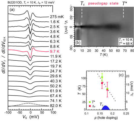
Figure 26 reproduces the -dependence of the DOS obtained by Kugler et al. (2001) on a slightly overdoped sample. The spectral features are less sharp than in Bi2212 and show a slight scattering, thus requiring the averaging over a large number of spectra to extract the general behavior. In spite of that, the data clearly shows that the pseudogap exists also on the overdoped side, and that its magnitude is comparable to the superconducting gap. Furthermore, it is obvious that the gap magnitude is to first approximation -independent. The overall DOS evolution is thus similar to what has been observed in Bi2212 (Figs. 22b, 24, and 25), although Bi2201 has a much lower and a smaller superconducting gap.
The -interval of the PG state is extremely large compared to the superconducting one, as illustrated in Fig. 26b. There is a factor 7 between and , the same as between and . thus scales with . This important observation is confirmed in a strongly underdoped sample, although the uncertainty on is much larger due to sample inhomogeneity (see Table 2).
Based on this data, Kugler et al. (2001) draw a tentative doping phase diagram for Bi2201 (Fig. 26c), illustrating that the PG phase extends significantly over the superconducting dome. This is particularly obvious in the overdoped regime and highlights that in this compound is strongly suppressed. For pure Bi2201 is about 13 K Vedneev et al. (1999); Gorina et al. (1998). The reasons for such a low relative to the gap are most probably disorder and strong phase fluctuations. Whether this anomalous loss of phase coherence is a hallmark of single-layer compounds remains an open issue. Preliminary results on La-doped Bi2201 (slightly underdoped, Kugler, 2000) showed gap magnitudes comparable to pure Bi2201, but for a as high as 29 K ( K, Ando et al., 2000). This suggests that La-doping does not change the pairing energy but rather favors phase coherence. It yields a reduced gap of the order of 10, which is consistent with Bi2212 and restores the superconducting phase accordingly to the generic phase diagram shown in Fig. 14, where the PG state is less dominant on the overdoped side. These findings point out that in the case of HTS, the relation between and is much more robust than the relation between and (see Sec. VI.1.5).
VI.1.3 The case of Y123 and Nd123
We finally turn to the -dependence of compounds having both CuO2 planes and CuO chains, in particular Y123 and Nd123. Figure 27a shows the results obtained by Maggio-Aprile et al. (2000) on optimally-doped Y123. The coherence peak position, hence the superconducting gap, remains constant with rising temperature, which is consistent with the Bi-based compounds. In contrast, the gap progressively fills up and eventually closes at the bulk , demonstrating that there is no signature of any pseudogap above the bulk in optimally-doped Y123. Very similar results were reported on Nd123 Nishiyama et al. (2002) as shown in Fig. 27b. These observations are consistent with results from other techniques (see review by Timusk and Statt, 1999). Thus in spite of the fact that Y(Nd)123 and Bi2212 have the same , they display a very different behavior with respect to the pseudogap. A possible key for understanding this difference is that Y(Nd)123 is much less anisotropic and appears to be much closer to the BCS limit than Bi2212 Junod et al. (1999). Furthermore the reduced gap values for optimally-doped Y123 () and Nd123 () are closer to the -wave BCS ratio (). The consequence is that Y(Nd)123 is less affected by superconducting fluctuations than Bi2212, thus possibly explaining the absence of a pseudogap. Another major difference comes from the CuO chains. How far these chains could prevent the existence of a pseudogap remains to be elucidated.
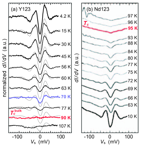
Besides these differences, Fig. 27a reveals other interesting aspects. A clear dip-hump feature is observed at about meV. This structure looks similar to what is seen in Bi2212 (see Sec. V.2) and it consistently disappears as approaches . Maggio-Aprile et al. (2000) showed that this disappearance is not due to thermal smearing, suggesting that the dip is related to the superconducting state. In fact, it turns out that the dip disappears at 70 K where the spectral line shape strongly resembles the Bi2212 spectrum at (Figs. 22 and 24). This could indicate that at the surface of Y123 the coherent superconducting state disappears at about 70 K and that above, a PG state exists up to 90 K. The explanation would be that the surface is different from the bulk in Y123 due to a higher effective anisotropy at the surface Meingast et al. (2001). However, this interpretation remains speculative since the gap signal above 70 K is too weak to make a decisive statement. A discussion of the doping phase diagram of Y123 is presented in Sec. VI.3.
VI.1.4 The case of electron-doped cuprates
A crucial question for understanding the microscopic mechanism of HTS is to what extent electron-doped cuprates R2-xCexCuO4-y (RCCO, ) are similar to hole-doped HTS. The specific issue of the existence of the pseudogap has been investigated using various tunneling techniques, although only very few reports exist. In Fig. 28a we reproduce STS data obtained on optimally-doped NCCO single crystals by Hayashi et al. (1998a). These results were confirmed by grain-boundary junction tunneling (GBJT) on optimally-doped NCCO and PCCO thin films by Kleefisch et al. (2001) (Fig. 28b). The general behavior is very similar to Y123 or Nd123, with the main conclusion that no pseudogap is observed at optimal doping.
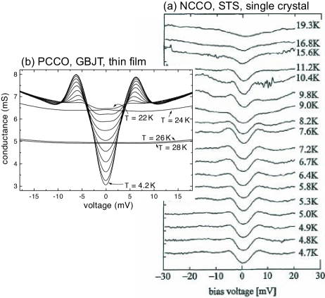
In contrast, when driving the superconductor into the normal state by applying a magnetic field, a clear PG spectrum appears which has the same magnitude as the superconducting gap at zero field Kleefisch et al. (2001); Biswas et al. (2001). This is consistent with what is observed in Bi2212 vortex cores (Sec. VI.2.1). Alff et al. (2003) investigated how this pseudogap evolves with doping and determined . They observed that has a similar doping dependence to that of the hole-doped copper oxides, however with the important difference that in the investigated doping range. The authors concluded that in electron-doped cuprates the PG phase coexists and competes with superconductivity and mentioned the possible existence of a quantum critical point.
VI.1.5 Scaling properties: pseudogap versus superconducting gap
An important step towards understanding the PG origin is to search for relations between the gap and pseudogap magnitude, as well as between and . The superconductors described in this section are an ideal stage for such an analysis. Bi2212 acts as a template, whereas Bi2201 and Y123 allow to test if the scaling behaviors are generic. Bi2201 presents the advantage to have a crystal structure similar to Bi2212 but radically different superconducting parameters and , whereas Y123 and Bi2212 have comparable ’s but different crystal structures.
Figure 29a compares the low- superconducting DOS and the PG spectrum measured slightly above in Bi2212 and Bi2201. The superconducting gap clearly increases with underdoping (see also Fig. 15) and the pseudogap behaves exactly the same in both compounds. Moreover, the relative amplitude of these two gaps is nearly the same in both compounds independent of doping as shown in Fig. 29b Kugler et al. (2001). This consistency is remarkable since the energy scale given by varies by about 400%. Whether the scaling between the pseudogap and the superconducting gap observed in Bi-cuprates also applies to Y123 remains to be seen. This question may be answered by investigating the DOS -dependence of underdoped samples, where other techniques have suggested that a pseudogap exists (see review by Timusk and Statt, 1999).
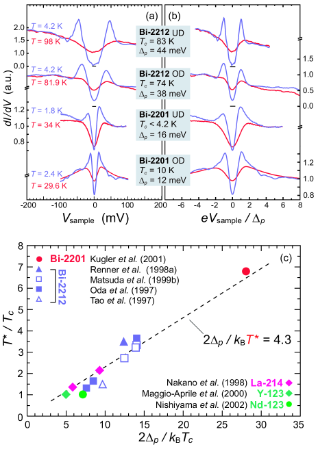
The existence of a scaling relation between and was first noticed by Oda et al. (1997) in Bi2212 and by Nakano et al. (1998) in La214.171717In both cases the values where determined by in-plane resistivity measurements. As shown in Fig. 29c, the same scaling law also holds for Bi2201 Kugler et al. (2001), although is 2–3 times larger. Optimally-doped Y123, where Maggio-Aprile et al. (2000), also fits into the picture. This consistency among various compounds is strong evidence that the scaling is robust. Moreover, the graph reveals that , which corresponds to the BCS -wave relation with playing the role of . This finding clearly supports the idea that is the mean-field BCS temperature and reflects the interaction energy leading to superconductivity.
| Compound | (K) | (meV) | (K) | Reference | |||
| Bi2212b | 60 | UD | Oda et al. (1997) | ||||
| Bi2212c | 77 | UD | Dipasupil et al. (2002) | ||||
| Bi2212c | 82 | UD | Dipasupil et al. (2002) | ||||
| Bi2212 | 83 | UD | Renner et al. (1998a) | ||||
| Bi2212 | 90 | OP | Matsuda et al. (1999b) | ||||
| Bi2212b | 88 | OP | Oda et al. (1997) | ||||
| Bi2212d | 87 | ? | Tao et al. (1997) | ||||
| Bi2212 | 84 | OD | Matsuda et al. (1999b) | ||||
| Bi2212c | 82 | OD | Dipasupil et al. (2002) | ||||
| Bi2212 | 81 | OD | Matsuda et al. (1999b) | ||||
| Bi2212b | 81 | OD | Oda et al. (1997) | ||||
| Bi2201 | UD | M. Kugler (unpublished) | |||||
| Bi2201 | 10 | OD | Kugler et al. (2001) | ||||
| Y123 | 92 | OP | Maggio-Aprile et al. (2000) | ||||
| Nd123 | 95 | OP | Nishiyama et al. (2002) | ||||
| La214b | UD | Nakano et al. (1998) | |||||
| La214b | OD | Nakano et al. (1998) | |||||
| The identification as underdoped or overdoped is the one given by the authors. | |||||||
| is determined by in-plane resistivity measurements. | |||||||
| SIS point-contact break-junction. | |||||||
| Pb/Bi2212 planar junction. | |||||||
VI.2 The pseudogap at low temperatures
Various STS studies demonstrated that the characteristic PG signature is not only observed above , but also occurs at low temperatures inside vortex cores Renner et al. (1998b) and on strongly disordered surfaces Cren et al. (2000); McElroy et al. (2004).
VI.2.1 The pseudogap inside vortex cores
The spatial dependence of the LDOS at low temperatures and in magnetic fields has been investigated by different groups on Bi2212 Renner et al. (1998b); Pan et al. (2000a); Hoogenboom et al. (2000b) and Y123 Maggio-Aprile et al. (1995, 1997); Shibata et al. (2003b) and revealed the unconventional spectral signature of the vortex cores in these compounds, as discussed in detail in Sec. VII. Here we focus on the relation between vortex-core spectra observed on Bi2212 and the pseudogap above .
Renner et al. (1998b) measured the evolution of the spectra when the tip is moved across a vortex core (VC) on a Bi2212 surface (Fig. 30a). Outside the VC the spectra do not depend on tip position and present well-defined coherence peaks and the characteristic dip-hump. Moving into the VC the coherence peak at negative bias is suppressed over a typical distance of 10 Å, whereas the peak at is reduced and shifts to slightly higher energy. This behavior is strikingly similar to the -dependence of the DOS when crossing , as illustrated in Fig. 30. In Fig. 30c the VC spectrum is numerically smeared to the temperature where the pseudogap is measured, showing again the similarity of both line shapes. From this Renner et al. (1998b) conclude that the LDOS measured at the vortex center is the normal-state PG signature, and that the spectrum measured above is essentially the thermally-smeared low- LDOS. This implies that the PG magnitude, like the superconducting gap (Fig. 23), is -independent. Furthermore, as shown in Fig. 30c, the VC gap magnitude is to first approximation equal to the superconducting gap measured just outside the core. Renner et al. (1998b) also showed that these findings are doping independent and therefore consistently obey the scaling properties derived for the pseudogap measured above (Fig. 29).
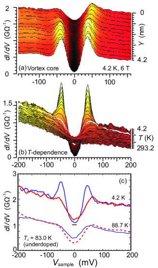
The correspondence between the normal-state pseudogap and the vortex-core spectra, as well as the doping and -dependence of the spectra reviewed respectively in Sec. V and VI.1, have important consequences and raise crucial questions with respect to the origin of the pseudogap.
Does the superconducting state develop on top of a gapped conductance background originating from an independent PG state, similar to the charge-density wave gap observed in dichalcogenides (see e.g. Coleman et al., 1992; Wang et al., 1990)? If the pseudogap would have an origin different from superconductivity, then the normal-state gap would not necessarily need to have the same amplitude as the superconducting gap. This scenario could explain why the pseudogap is observed in the vortex cores, but is difficult to reconcile with the fact that the two gaps scale with each other as the doping is changed.
An important question related to the correspondence between the pseudogap and the vortex core is whether the PG state between and is due to fluctuating vortices. Thermal transport experiments by Wang et al. (2001) support this idea. They found an anomalous Nernst signal above in La214 and Bi2201, which they attributed to vortex-like excitations. They pointed out that this regime penetrates deep into the PG phase and appears predominantly in underdoped samples. They interpreted these results in terms of strong fluctuations between the PG state and the -wave superconducting phase Emery and Kivelson (1995); Norman et al. (1998); Franz and Tešanović (2001); Lee and Wen (2001). These vortex-like excitations could be electronic excitations specific to the PG state or, as suggested by tunneling data (Renner et al., 1998b, Fig. 30), they could be Abrikosov vortices of the superconducting condensate formed in the normal state by phase fluctuations. In the latter scenario the pseudogap would have the same origin as superconductivity, raising the interesting question of its magnetic field dependence.
The field dependence of the pseudogap above has not yet been investigated systematically by STS.181818Ng and Gupta (2000) investigated Bi2212 using PC-BJT. No field dependence of the pseudogap was observed up to 1.1 T; Krasnov et al. (2001) investigated Bi2212 mesas by IJJT. The spectral signature they attributed to the pseudogap is invariant at least up to 14 T. Note however that this structure has been attributed to an artifact of Joule heating in the mesas (see Sec. VI.1.1). Anagawa et al. (2003) performed similar investigations up to 9 T. They observe that both the pseudogap structure and the superconducting gap are essentially field independent. However, Hoogenboom et al. (2000b) showed on Bi2212 at 4.2 K that the energy of the core states and the superconducting gap in between cores scale and are field independent, at least at moderate fields up to 6 T (Sec. VII). The PG state under fields as high as 60 T has been investigated by -axis transport measurements in Bi2212 by Krusin-Elbaum et al. (2003). These experiments showed that above T the -axis resistivity, which is believed to be proportional to the Fermi-level DOS, increases notably, indicating that the pseudogap is filling up with increasing field. Krusin-Elbaum et al. also determined the pseudogap closing field , which for an overdoped sample extrapolates to about 90 T at K. Remarkably, scales with as , hence with (Sec. VI.1.5). These results fit well into a picture where the PG state is formed of incoherent pairs, that eventually break at the depairing field .
In this context, we mention grain-boundary junction tunneling experiments performed on the electron-doped cuprates NCCO and PCCO Kleefisch et al. (2001); Biswas et al. (2001). The suppression of superconductivity by a strong magnetic field results in a PG-like spectrum at (See also Sec. VI.1.4). Kleefisch et al. (2001) also demonstrated that the pseudogap closes at a field corresponding to the Clogston paramagnetic limit Clogston (1962); Yang and Sondhi (1998).
VI.2.2 The pseudogap on disordered surfaces
Over the past years many studies focused on the spatial variations of the LDOS at the nanometer scale under the influence of disorder. Here we discuss the local observation of the pseudogap at low temperatures and zero magnetic field in Bi2212 thin films Cren et al. (2000) which have a high degree of structural disorder, in UD Bi2212 single crystals Howald et al. (2001) where disorder has been introduced intentionally by local damage, and in inhomogeneous samples where disorder is presumably due to a local variation in oxygen concentration McElroy et al. (2004).
Figure 31a shows the evolution of the LDOS as the tip is moved out of a superconducting region on a Bi2212 thin film Cren et al. (2000): a gap with well-defined coherence peaks abruptly changes into a spectrum with the same gap magnitude, and which is identical to the one observed at and in the vortex cores. Moving further away from this pseudogapped zone the spectra finally become semiconductor-like (not shown in Fig. 31a), indicating that strong disorder is indeed present. The gap-pseudogap transition occurs over roughly 10 Å, consistently with the spectral evolution across a vortex core (Fig. 30a and Sec. VII). This characteristic length is of the order of and sets the scale for the loss of superconducting phase coherence. Similar results were obtained on Pb-doped Bi2212 single crystals Cren et al. (2001) and on an intentionally “damaged” Bi2212 single crystal Howald et al. (2001), as shown in Fig. 31b (spectrum F). These experiments show that in strongly disordered samples superconducting and pseudogapped regions can locally coexist.
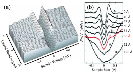
Many other experiments on native and generally UD Bi2212 surfaces also demonstrated patches with variable superconducting characteristics Pan et al. (2001); Howald et al. (2001); Lang et al. (2002); Matsuda et al. (2003); Kinoda et al. (2003); McElroy et al. (2004). However, as illustrated in Fig. 32b, these results show a central difference: instead of presenting a constant gap magnitude when crossing the limits of a patch, the coherence peaks shift to considerably higher energies, they gradually broaden and decrease in intensity to eventually end up in a PG-like DOS. This behavior is characteristic for local variations of the oxygen content, as demonstrated by Pan et al. (2001) (Fig. 16d). In terms of the doping phase diagram, these experiments show, on a local scale, how the DOS evolves when reducing the doping level (Fig. 32c). This is in clear contrast with the observations by Cren et al. (2000), who found that the gap magnitude remains constant. These authors interpreted their results using a theoretical model by Huscroft and Scalettar (1998). It shows that in the presence of strong disorder, the phase coherence is lost, while the pairing amplitude which manifests itself as the pseudogap, is not necessarily suppressed.
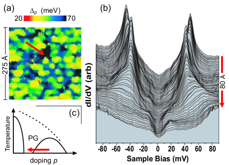
The systematic study of microscopic inhomogeneities in the LDOS at different dopings on Bi2212 by McElroy et al. (2004) revealed that the total area showing regions with large gap values increases with underdoping. For strongly underdoped samples, regions appear where the coherence peaks are absent. The authors claim that in those regions all spectra are identical to each other, and that no changes are observed on further underdoping. Instead, the total area covered by such regions increases. McElroy et al. (2004) therefore conclude that they observed a limiting class of spectra and identified it as the zero-temperature pseudogap (ZTPG). Similar spectra were observed by Hanaguri et al. (2004) on heavily underdoped and even non-superconducting Ca2-xNaxCuO2Cl2. As illustrated in Fig. 33c, these spectra have a V-shaped gap with a broad peak at positive bias, and resemble the PG spectrum described earlier, however for an extremely underdoped region, since the peak at positive bias is around 150 mV. It is suggested that these spectra characterize the DOS between the superconducting dome and the antiferromagnetic phase Hanaguri et al. (2004). In contrast to the -dependence of the DOS (Sec. VI.1.5) where the pseudogap and superconducting gap have the same magnitude, we emphasize that in the case described in Fig. 33a the ZTPG does not scale with the superconducting spectrum since they do not correspond to the same doping level: the superconducting spectra are typical of optimally or slightly underdoped regions, whereas the ZTPG spectra correspond to extremely underdoped regions. This aspect is clearly seen in Fig. 32.
These observations suggest that there exist two types of disorder which have distinct spectral signatures: (i) disorder which does not change the local doping level, hence the gap magnitudes are the same in both the superconducting and pseudogap regions; (ii) disorder due to a locally varying oxygen concentration, hence the observed pseudogap will correspond to an extremely underdoped sample.
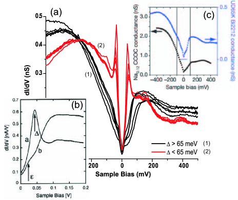
As first pointed out by Howald et al. (2001) and later by McElroy et al. (2005a), the low-energy features of the spectra shown in Fig. 33a and b coincide up to roughly 20 meV, above which a kink occurs in the ZTPG. This might indicate that the so-called ZTPG has two components: a first component originating from the nodal points with coherent -wave quasiparticles at energies below the kink, and a second one at higher energies with incoherent quasiparticles predominantly from the anti-nodal points, yielding the pseudogapped envelope due to the reduced quasiparticle lifetime. Other interpretations in terms of phase separation between “good” and “bad” superconducting regions have also been proposed Howald et al. (2001); Lang et al. (2002). The issue of a two-component behavior is discussed in more detail in Sec. VIII in relation with the spatial modulations of the LDOS.
VI.3 The doping phase diagram
Conventional BCS superconductors are characterized by their , which is closely related to the pairing energy via the coupling constant . The phase diagram of HTS is much more complex (Fig. 14). The superconducting gap seems to be unrelated to and a new state—the PG state—appears above as discussed in the previous paragraphs. Although it is generally accepted that the pseudogap is intimately related to the occurrence of high , there is currently no consensus as to its nature (see reviews by Timusk and Statt, 1999; Phillips et al., 2003). Two alternative phase diagrams, depicted in Fig. 34, are generally proposed. Either merges with on the overdoped side, or crosses the superconducting dome and possibly falls to zero at a quantum critical point (QCP).
Different scenarios can be associated with different phase diagrams. For instance, if the pseudogap would be the signature of a phase-disordered -wave superconductor, a phase diagram like the one shown in Fig. 34a would naturally result, although in this scenario the line could also cross the superconducting dome. In the scenario that the pseudogap would be a phenomenon different and largely independent of superconductivity, like a charge density wave, it has been proposed that the dome results from the competition of the two phenomena, the pseudogap winning out at low doping and superconductivity at higher doping. In such a scenario it is expected that would fall below roughly at optimal doping and end in a QCP hidden below the dome as shown in Fig. 34b. If this would be the correct explanation, the phase diagram shown in Fig. 34b should be a universal phase diagram. It was in fact for a long time assumed that the pseudogap was associated with the underdoped region of the phase diagram, since this seems to be the case for Y123. However, STS has clearly shown that for Bi2212 Renner et al. (1998a) and Bi2201 Kugler et al. (2001) the pseudogap exists also in overdoped samples and that the phase diagram for these compounds is of the type shown in Fig. 34a. Therefore STS has ruled out the phase diagram in Fig. 34b as a universal phase diagram for HTS materials.
Although the phase diagram has not yet been investigated systematically by tunneling spectroscopy, results obtained so far and discussed in this section already allow to draw some conclusions for Bi2212 and Bi2201: (i) the superconducting gap and the pseudogap are -independent, (ii) they have the same amplitude, (iii) the PG temperature increases monotonically when underdoping and scales with , and (iv) the pseudogap clearly exists in the overdoped region. These results obtained by STS—a method which probes directly the quasiparticle DOS—give strong support to the scenario depicted in Fig. 34a. This picture is corroborated by ARPES (see review by Damascelli et al., 2003, p. 520) and by various bulk techniques for several other cuprates (La214, Y124, Hg1223, Tl2201), as shown in Fig. 35. There are compounds, however, which deviate from the diagram of Fig. 34a. In Bi2201 the phase fluctuations seem to suppress even in the strongly overdoped region (Fig. 26c). In the case of Y123 (Sec. VI.1.3) the superconducting gap scales with Yeh et al. (2001). Furthermore, STS data at optimal doping does not reveal any clear pseudogap Maggio-Aprile et al. (2000), suggesting that the line is shifted towards the underdoped side. This is consistent with the early NMR experiments Warren et al. (1989); Alloul et al. (1989) and with a recent high-resolution dilatometry study by Meingast et al. (2001). These authors showed that phase fluctuations dramatically suppress from its mean-field value in UD Y123, whereas for overdoped samples . Thus exhibits a similar doping dependence as , suggesting that the pseudogap in Y123 is due to phase-incoherent Cooper pairs. Particularly interesting in this regard are the recent thermal conductivity measurements of Sutherland et al. (2005) which indicate the presence of -wave like nodal fermions even outside the superconducting dome of Fig. 34a. The presence of such nodal excitations provides strong support for the picture of the pseudogap as a superconducting ground state disordered by strong quantum phase fluctuations which nonetheless maintains a robust -wave pairing amplitude Franz and Tešanović (2001). In contrast, results obtained using other bulk techniques like transport, heat capacity, and infrared spectroscopy tend to favor the QCP scenario (see e.g. Tallon and Loram, 2001). No consensus is yet reached on this debate, which involves the non-trivial question of what each experimental technique is effectively attributing to the pseudogap and how these characteristics are related to each other.
From the point of view of tunneling, which gives the most direct access to the pseudogap, the results discussed here for hole-doped cuprates give strong support to the idea that the pseudogap is a precursor of the superconducting gap, reflecting fluctuating or non-coherent pairs. However, in the case of electron-doped HTSs more investigations are needed to reach a general view. The data available at present have been interpreted in terms of a QCP scenario Alff et al. (2003) as briefly mentioned in Sec. VI.1.4.
VI.4 Summary
Scanning tunneling spectroscopy allowed to directly visualize the existence of a pseudogap in the high-temperature DOS of Bi2212 and Bi2201. As the temperature is raised from the superconducting gap remains constant and smoothly evolves into the pseudogap across . The coherence peaks are abruptly reduced at giving rise to a generic PG spectrum. Above , the pseudogap is gradually filling up and remains essentially constant, with an apparent tendency to increase at higher temperature before vanishing at the crossover temperature .
The generic PG spectrum measured at in Bi2212 presents the following hallmarks: (i) the pseudogap and the superconducting gap have a comparable magnitude and scale with each other as a function of doping; (ii) the coherence peak at negative bias is completely suppressed; (iii) the coherence peak at positive bias is strongly reduced and shifts to slightly higher energies; (iv) the zero-bias conductance is increased. Furthermore (v) this PG spectrum is observed on both underdoped and overdoped samples, and (vi) the PG temperature scales with for all doping levels. These characteristics are common to Bi2212 and Bi2201 in spite of their radically different superconducting parameters. Furthermore, the PG signature is also observed at low temperatures in vortex cores and on disordered samples, where phase coherence is reduced or suppressed. Finally, it appears that for several HTS cuprates the values of and measured by STS roughly obey the -wave BCS scaling law, , consistent with other experimental techniques.
VII Imaging of vortex matter and core structure by STS
The vortex state study provides a very direct access to the fundamental properties of superconductors. The electronic structure of the vortex cores, as well as the interaction between the flux lines, are intimately connected with the nature and the behavior of the charge carriers. STS offers unique capabilities to investigate these properties. STS provides a way to detect the individual flux lines and visualize the vortex distribution in real space, as well as the structure of the cores. In addition, the probe can access the electronic excitations within the cores, revealing important and often unexpected properties of the superconducting pairing states.
Ten years after the theoretical prediction of type-II superconductivity by Abrikosov (1957), real-space imaging of vortices was achieved using Bitter decoration in lead Essmann and Träuble (1967). Various techniques of vortex imaging in real space have been developed since then, all relying on the magnetic field generated by the flux lines, and hence restricted to relatively low fields. In the case of extreme type-II superconductors like HTS, where the penetration depth amounts to hundreds of nanometers, the magnetic imaging contrast starts to be damped at fields not exceeding very much .
A breakthrough occurred when Hess et al. (1989) used STS to map the vortex lattice of NbSe2, by detecting systematic spatial variations of the tunneling conductance. Since the latter occur over distances of the order of the coherence length around the vortex center, this technique can in principle be used up to fields where the cores start to overlap, i.e. . In practice, because of the small size of the cores, the relatively slow sampling and the limited field of view of the instrument, vortex imaging by STS should be considered as a complementary tool to other vortex mapping techniques, especially at very low fields or in the case of vortex dynamics studies.
This section will start with a brief overview of vortex matter studies by STS. The focus will then be set on the specific electronic signature of the vortex cores. One of the most important observation is that the vortex cores in Bi2212 exhibit pseudogap-like spectra, revealing the non-BCS character of superconductivity in this compound. The existence of low-energy discrete states in both Y123 and Bi2212 is another surprising property of the cores. The properties of the vortices in conventional BCS superconductors will also be presented, in order to establish comparisons with the striking electronic signatures found in HTS.
VII.1 Vortex matter imaging by STS
STS imaging of the vortices relies on the fact that their cores affect the quasiparticle excitation spectra. Images are usually obtained by mapping the tunneling conductance in real space at a particular bias voltage (see Sec. II). The imaging contrast depends strongly upon the chosen bias voltage, since the spatial variations of the tunneling conductance close to the vortex are usually energy dependent. Consequently, the visual aspect of the vortex cores in the images depends on the mapping energy. The performances of the technique are also inherently related to the quality of the sample surfaces, since the spectroscopic signatures of superconductivity are easily affected by a non adequate surface layer (Sec. IV). Inhomogeneities like structural defects, chemical adsorbates, impurities, or electronic inhomogeneities will generally perturb the detection of individual vortices.
Vortex imaging by STS finds an obvious interest in the study of the spatial distribution of the flux lines. Most conventional superconductors have an isotropic BCS order parameter, and when pinning is not effective, vortices arrange in a regular lattice. When pinning is more relevant, vortex lattices become disordered. The STS observation of the flux lines on BCS compounds confirms these expectations. In addition, STS imaging provides information on the shape of the cores. Both informations give a direct access to the anisotropy of the superconducting state.
Because obtaining surfaces with homogeneous electronic characteristics is difficult, vortex imaging by STS was achieved on only a few materials, essentially conventional superconductors. For HTS, degradable surfaces and the very small coherence lengths imply that the superconducting spectral characteristics may be affected by the nature of the topmost layer. The technological developments allowing the synthesis of large and ultra pure single crystals largely contributed to the recent breakthroughs in spectroscopic studies and vortex imaging of some HTS.
VII.1.1 NbSe2 and other conventional superconductors
With easily cleavable planes and a reasonably high (7.2 K), NbSe2 is an ideal candidate for vortex studies using STS. The first experiments of Hess et al. were followed by many other studies Renner et al. (1991); Behler et al. (1994).
The standard way to detect vortices in NbSe2 is to map the conductance measured at the energy of the coherence peaks. An example is shown in Fig. 36a revealing vortices arranged into a perfect hexagonal lattice with a lattice parameter of nm. The expected inter-vortex spacing is yielding nm for T. Since the magnetic profile of a single flux line in Fig. 36a extends over about one quarter of the total image, techniques sensitive to the magnetic field would be, in the same conditions, incapable to distinguish individual vortices. The vortex cores look isotropic with an apparent radius of 15 to 20 nm, larger than the coherence length of NbSe2 estimated to be 7.7 nm from critical field anisotropy measurements de Trey et al. (1973).
The relatively long acquisition times do not preclude vortex dynamics studies by STS, provided that the flux line motion is sufficiently slow. Renner (1993) observed vortices with an elongated shape due to a slow motion of the lattice during the line by line scanning of the tip. After some time, this motion stopped and the vortex cores appeared perfectly isotropic. More recently, much faster vortex imaging was achieved by controlling the tip position, without interrupting the feedback loop, using a voltage close to the gap energy, rather than the commonly-used biases in the CITS technique Troyanovski et al. (1999, 2002).
Disordered lattices in irradiated NbSe2 samples illustrated the pinning of vortices by columnar defects Behler et al. (1994). This observation was helped by the fact that the coherence length in NbSe2 is much larger than the size of the defects. When the cores and the defects have similar sizes, the spectroscopic signatures of the cores may be masked by the defects, and thus difficult to distinguish (see e.g. Zn-doped Bi2212 by Pan et al., 2000a).
A hexagonal vortex lattice was also seen in MgB2 single crystals, as shown in Fig. 36b Eskildsen et al. (2002). The expected vortex spacing of 109 nm is readily verified in the image. More surprisingly, DeWilde et al. (1997a) found a square vortex lattice in the borocarbide LuNi2B2C (Fig. 36c) at a field of 1.5 T. The expected spacing for a square lattice, is again respected (37 nm at 1.5 T). The square symmetry was explained in a Ginzburg-Landau theoretical approach, considering a fourfold perturbation term in the free energy arising from the underlying tetragonal structure of the crystal DeWilde et al. (1997b). A transition from a distorted hexagonal lattice at low fields to a square lattice at high fields was predicted, and experimentally confirmed by small angle neutron scattering Eskildsen et al. (1997). Later, this transition was directly observed by STS in another borocarbide compound, YNi2B2C Sakata et al. (2000), and in the cubic A15 compound V3Si Sosolik et al. (2003).
VII.1.2 High-temperature superconductors: Y123 and Bi2212
The behavior of vortices in HTS cuprates differs radically from what is observed in BCS superconductors. At first sight, the high ’s and the large superconducting gaps make them ideal compounds for STS, since for most of them, the electronic characteristics can be probed at 4.2 K or above, and the characteristic DOS features are situated at relatively high energies. But because of difficulties in preparing surfaces with sufficient homogeneity, the study of vortices by STS remained a considerable challenge. Up to now, imaging of vortices has been possible only in Y123 and Bi2212. The very small coherence length in these materials have two direct observable implications. First, the vortex cores are tiny in comparison to conventional superconductors, and thus difficult to localize. Second, the vortices get easily pinned by defects. As a consequence, at the relatively high fields which are suitable for STS, flux lines lattices show no perfect order in HTS.
Examples of vortices imaged with STS in a 6 T field in both Y123 and Bi2212 are presented in Fig. 37. In Y123 the vortices arrange in a slightly disordered oblique lattice (Fig. 37a). In Bi2212 they are more disordered (Fig. 37b). Note that the entire scan range of Fig. 37 fits into a single vortex core of Fig. 36b, graphically illustrating the small size of the cores in HTS.
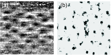
Y123
Y123 was the first non-conventional superconductor whose vortex lattice could be investigated by STS, and this was achieved by Maggio-Aprile et al. (1995) on as-grown surfaces. Since then, two other groups reported the STS observation of flux lines in Y123, either on as-grown surfaces Hubler et al. (1998), or on chemically etched surfaces Shibata et al. (2003b). Fig. 38a shows an image acquired in optimally-doped Y123 ( K). The observed vortex density matches the 6 T applied field. The lattice shows a local oblique symmetry, with an angle of about 77∘. Vortex cores reveal an apparent radius of about 5 nm, but systematically present an elliptical shape with an axis ratio of about 1.5 (see Fig. 38a). Maggio-Aprile et al. (1995) noticed that this distortion is independent of scanning direction and not related to any flux line motion, and they ascribed it to the -plane anisotropy of Y123.
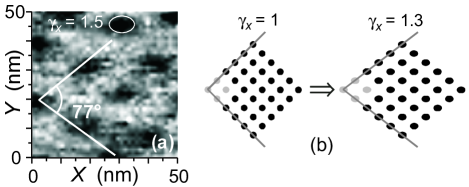
In the framework of an anisotropic Ginzburg-Landau model, the observed oblique lattice in Y123 can be interpreted as a square lattice distorted by an anisotropy factor of , or as a hexagonal lattice distorted by an anisotropy factor of . Since it is expected that the anisotropy controlling the distortion of the lattice is also responsible for the intrinsic distortion of the cores, the observed value of for the latter led Renner et al. (1996) to conclude that the lattice corresponds to a deformed square lattice as illustrated in Fig. 38b. Similar anisotropy factors have been derived from penetration depth measurements in Y123 Zhang et al. (1994). At analog magnetic fields, neutron scattering measurements showed similar distortions Keimer et al. (1994). More recent neutron scattering investigations evidenced a continuous transition from a distorted hexagonal to a nearly perfect square lattice at high fields Brown et al. (2004). Square vortex lattices can be expected in a number of situations where a four-fold perturbation field acts. In particular, a square lattice was predicted for -wave superconductors Won and Maki (1995); Affleck et al. (1997). It is not yet clear whether the tendency to order into a square lattice at high field is due to the -wave symmetry of the order parameter, or to other factors. On the other hand, Bitter decoration measurements at low fields revealed a regular Gammel et al. (1987); Vinnikov et al. (1988); Dolan et al. (1989a) or slightly distorted Dolan et al. (1989b) hexagonal lattice, as expected at low vortex density.
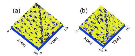
The disorder observed in the vortex lattice underlines the influence of strong pinning in compounds with small coherence lengths. In Y123, a substantial vortex creep is observed after switching on the magnetic field, with flux lines continuously moving for a couple of days. The influence of twin boundaries on pinning in Y123 single crystals has stimulated various debates and investigations Gammel et al. (1992); Vlasko-Vlasov et al. (1994); Welp et al. (1994); Crabtree et al. (1996); Herbsommer et al. (2000). STS measurements demonstrate that the twin boundaries act as very efficient barriers, blocking the movements of the flux lines perpendicular to the twin plane. This phenomenon is illustrated in Fig. 39a, which shows vortices mapped out in a field of 3 T on both sides of a twin boundary Maggio-Aprile et al. (1997), seen as the dark line running along the direction. Vortices are found on both sides with the same average density. The anisotropic shape of the cores is rotated by 90∘ between both domains, demonstrating that the dark line separates two regions with inverted and crystallographic axes. The field was then reduced to 1.5 T, and a piling up of flux lines on the left side of the twin boundary was observed, corresponding to a field of 2.5 T, substantially higher than the applied field. The right side showed a vortex free region extending over more than hundred nanometers (Fig. 39b). The gradients of the magnetic field could be directly measured from the flux line distribution, and allowed the authors to estimate a current density close to the depairing current limit for Y123 (A/cm2). The dark line on the twin boundary was attributed to trapped vortices, too densely packed or mobile to be resolved.
Bi2212
In Bi2212, the quasiparticle spectra taken outside and inside the vortex cores show rather small differences (see Fig. 30). Renner et al. (1998b) imaged for the first time vortices in overdoped Bi2212 using negative energies. As seen in Fig. 40a the cores in Bi2212 are tiny, consistent with a coherence length of the order of a few atomic unit cells. They usually exhibit irregular shapes (see Sec. VII.3.2).
In the STS images, the vortices are distributed in a totally disordered manner, but with an average density matching the 6 T field Renner et al. (1998b). This can be understood since Bi2212, unlike Y123, has a nearly two-dimensional electronic structure and the vortices are therefore constituted by a stack of 2D elements (pancakes), weakly coupled between adjacent layers, and easily pinned by any kind of inhomogeneity. The observed disordered lattice fits into the commonly accepted vortex phase diagram for Bi2212, where the low-temperature high-field region is associated with a disordered vortex solid. At very low fields takes place an ordered Bragg glass phase, difficult to probe with STS because of the large inter-vortex distances. At 8 T, however, Matsuba et al. (2003a) observed a short-range ordered phase in Bi2212, presenting a nearly square symmetry almost aligned with the crystallographic directions (Fig. 40b).
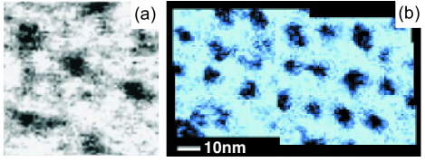
VII.2 Electronic structure of the cores
VII.2.1 BCS superconductors
In 1964 Caroli, de Gennes, and Matricon provided an approximate analytical solution of the Bogoliubov-de Gennes equations for an isolated vortex in a clean -wave superconductor. They predicted the existence of electronic states bound to the vortex at energies below the superconducting gap. These bound states form a discrete spectrum with a typical inter-level spacing . For most superconductors, this spacing is so small that the detection of individual bound states is hampered by the finite temperature and by impurity scattering. In NbSe2, is typically K, and so far, it was not possible to resolve an ideal discrete spectrum. Instead, a strong zero-bias conductance peak (ZBCP) is observed, understood as the continuous envelope of a set of low-energy states.
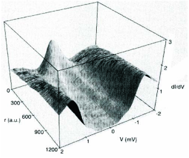
Hess et al. (1989) studied vortex cores by STS in pure NbSe2 single crystals at K, and observed features in agreement with theoretical expectations Shore et al. (1989). The progressive splitting of the ZBCP at a distance from the center provided another verification of the BCS predictions for vortex cores in -wave superconductors (Fig. 41). This splitting reflects the presence of many core states with different angular momenta . The lowest-lying state () has energy and maximum probability at , giving rise to the ZBCP at the vortex center. The energy of higher-angular momentum vortex states departs from zero as at low Caroli et al. (1964), and these states have maximum amplitude at a distance from the core center. In the LDOS, these latter states show up as one electron branch () and one hole branch () at energy and position . With increasing , the electron and hole branches approach the gap edges at , and merge asymptotically with the continuum of scattering states with energies . Thus the superconducting spectrum is eventually recovered outside the core, at –. These observations were successfully described by a complete numerical solution of the Bogoliubov-de Gennes equations for an isolated -wave vortex Gygi and Schlüter (1990b); Gygi and Schlüter (1991).
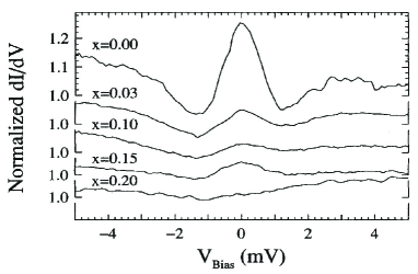
In dirty superconductors, quasiparticle scattering mixes states with different angular momenta, and the zero-bias peak transforms into a quasi-normal (flat) DOS spectrum when the quasiparticle mean free path is smaller than the coherence length. This effect was observed by STS in Ta-doped NbSe2 Renner et al. (1991), as shown in Fig. 42. The spectra were acquired in different Nb1-xTaxSe2 samples, each doped with a specific amount of tantalum. As seen in the figure, the low-energy spectra taken at the core center progressively lose the pronounced zero-bias feature, and for dopings show a nearly constant conductance reminiscent of the normal-state DOS.
DeWilde et al. (1997a) reported similar vortex-core spectra for LuNi2B2C (Fig. 43a), with a nearly constant tunneling conductance. Recently Nishimori et al. (2004) reported the observation of a zero-bias peak in pure samples of this compound. In the two-band superconductor MgB2, the vortex-core spectra acquired on the (001) surface show also a totally flat conductance (Eskildsen et al. (2002), Fig. 43b). This observation is more surprising, since the mean free path in MgB2 is believed to be much larger than the superconducting coherence length. The absence of a zero-bias peak was attributed to the fact that the -band is predominantly probed in this geometry. Since this band becomes superconducting through coupling with the -band, the presence of a flux line, suppressing the superconducting character of the -band, also affects the -band, which becomes metallic, with an energy independent DOS Eskildsen et al. (2002).
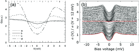
VII.2.2 High-temperature superconductors
Y123
The predictions and experimental confirmations of core bound states in BCS -wave superconductors raised important questions when the exotic properties of HTS were uncovered. Among these, the question of the electronic signature of the vortex cores in HTS was at the time completely open. The first answers came from measurements on optimally-doped Y123 single crystals by Maggio-Aprile et al. (1995). Fig. 44a shows a tunneling conductance map of a vortex recorded at an energy close to the positive coherence peak, and illustrates the suppression of the latter in the core region. The most striking observation comes from the conductance spectrum at the core center (Fig. 44b). Contrary to the case of conventional superconductors, the core spectra in Y123 neither reveal any broad zero-bias feature nor a flat conductance. Instead, a pair of low-energy peaks clearly emerging above the conductance background is observed at an energy of about meV. While both coherence peaks near meV disappear inside the core, a broad feature of reduced intensity persists at slightly higher energies (30–40 meV).
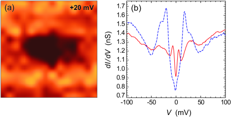
The observation of isolated core states at finite energy in Y123 appeared contradictory in various respects. On one hand, attempts to interpret the observed bound states like classical BCS -wave localized states failed for two reasons: first, it would imply an unusually small Fermi energy ( meV); second, there is a complete absence of energy dispersion at different positions within the core (Fig. 45). When the tip starts entering the core (=16.7 nm), the 20 meV coherence peaks progressively vanish, and the low-energy core states develop while the tip approaches the core center (=0). The energy at which the core states are observed does not vary, indicating that only one pair of localized states exists below the gap. Note that a weak low-energy structure persists in the spectra outside the vortex cores (see spectrum at nm in Fig. 45 and the dashed spectrum in Fig. 44b). A similar structure also exists in the absence of magnetic field (see Sec. V). Although the energy of this structure observed outside the cores is approximately the same as the core state energy, the question of its origin and the relation it has with the core state is still open.
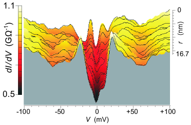
On the other hand, this observation does not fit with the -wave character of the cuprate compounds. Following the observation of anomalous core spectra in Y123, an important effort was dedicated to calculating the quasiparticle spectra in the vortex cores of -wave superconductors, where the presence of nodes in the order parameter changes the properties of the low-energy excitations. Based on the Bogoliubov-de Gennes Soininen et al. (1994); Wang and MacDonald (1995); Morita et al. (1997b); Franz and Tešanović (1998); Yasui and Kita (1999) or Eilenberger Ichioka et al. (1996, 1999) equations, it was shown that the vortex-core energy spectrum is continuous rather than discrete, and that the quasiparticles in the core are not exponentially localized as in -wave superconductors. The theoretical LDOS at the center of the core shows a broad peak at zero energy.
Therefore the observation of discrete states at finite energy is in contradiction with the -wave BCS picture. A possible magnetic origin of these states has been ruled out because (i) the Zeeman splitting can be estimated to be about ten times smaller than the measured energy of the states, and (ii) the peak energy position was found to be independent of the applied magnetic field. Finite-energy core states in Y123 were confirmed in more recent STS studies by Shibata et al. (2003b). Infrared absorption measurements Karraï et al. (1992) also clearly identified the existence of low-energy quasiparticle excitations, in quantitative agreement with all STS observations.
Bi2212
Vortex core spectroscopy in Bi2212 provided new insights into the debate concerning the origin of the pseudogap, starting with the STS measurements of Renner et al. (1998b) on both underdoped and overdoped Bi2212 single crystals. The evolution of the spectra across a vortex core in overdoped Bi2212 is shown in Fig. 46. When entering the core, the spectra evolve in the same way as when the temperature is raised above : the coherence peak at negative energy vanishes over a very small distance, the coherence peak at positive energy is reduced and shifts to slightly higher energies, and the dip/hump features disappear. The observation of such pseudogap-like spectra in the cores of Bi2212 is discussed in more details in Sec. VI.
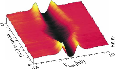
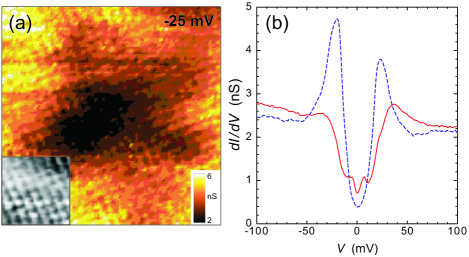
While the first vortex core investigations in Bi2212 focused on pseudogap aspects, Pan et al. (2000a) and Hoogenboom et al. (2000b) showed that weak low-energy structures were also present in the vortex core spectra. Fig. 47a shows a spectroscopic image, mapped out at meV, of a vortex core in slightly overdoped Bi2212. The full conductance spectra taken inside and outside the core are shown in Fig. 47b. Contrary to Y123, where the peaks clearly emerge in the core center, the core states appear in Bi2212 as weak peaks in an overall pseudogap-like spectrum. For slightly overdoped Bi2212, the energy of these states is of the order of meV. A slight increase of the zero-bias conductance is also systematically measured in the core center.
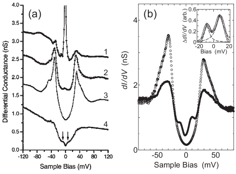
Various studies reported the observation of such states in Bi2212. Pan et al. (2000a) observed that vortices sitting away from impurity sites show core spectra with the low-energy gapped structure, as indicated with arrows in the bottom curve of Fig. 48a. These spectra are compared with the ones acquired on strong or weak impurities shown in the top two curves of Fig. 48a, where vortices are likely to be pinned. As a consequence, they deduce that the pair of localized states reflects an intrinsic character of the vortex cores. The systematic presence of core states in Bi2212 at different oxygen dopings was also reported by Matsuba et al. (2003a), shown in Fig. 48b. They observed an asymmetry of the peak heights, which they attributed to positively-charged vortices.
Hoogenboom et al. (2000b) investigated various samples where a large number of vortices showed the low-energy structures, measured at an energy independent of the position within the core, as shown in Fig. 49. We stress that later investigations Levy et al. (2005) showed that the intensity of the core-states peaks depends on the precise measurement position within the core (see Sec. VIII.3).
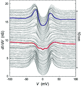
The low-energy core states observed in both Y123 and Bi2212 raise two important questions. Are the core states observed in Y123 and Bi2212 of the same origin? And how can these core states be understood within the framework of a -wave symmetry of the order parameter? In order to answer the first point, detailed core spectra studies were carried out in both Y123 and Bi2212. One first notes that the spectra acquired in both Y123 and Bi2212 cores present a similar shape. In addition, although they are much more pronounced in Y123, the low-energy structures behave similarly in both types of compounds: they do not disperse when measured at various distances from the center of the core (Figs. 45 and 49) and they are magnetic field independent Maggio-Aprile et al. (1995); Hoogenboom et al. (2001). The most striking fact comes from the scaling between the energy of the core state and the superconducting gap amplitude , as shown in Fig. 50. The correlation found between and for Y123 (optimal doping) and Bi2212 (various dopings) strongly suggests that the core states in the two compounds have a common origin. Moreover, since this correlation is linear (with a slope of about 0.3), the interpretation of these bound states as Caroli, de Gennes, and Matricon states of an -wave superconductor with a large gap to Fermi energy ratio can be ruled out, as one would expect a dependence.
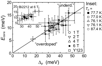
Many theoretical studies were undertaken in order to explain the observed electronic signatures of the vortex cores in HTS. The absence of a large ZBCP at the vortex center in Y123 and Bi2212 has been tentatively attributed to an anisotropic tunneling matrix element Wu et al. (2000). The general belief, however, is that the qualitative difference between the vortex-core spectra measured by STM in HTS and the spectra expected for a -wave BCS superconductor Soininen et al. (1994); Wang and MacDonald (1995); Franz and Tešanović (1998) reflects an intrinsic property of the superconducting ground state, which distinguishes this state from a pure BCS ground state, and is presumably related to the anomalous normal (pseudogap) phase. Franz and Tešanović (1998) showed that the admixture of a small magnetic-field induced complex component with symmetry Laughlin (1998) leads to a splitting of the ZBCP due to the suppression of the -wave gap nodes; as noted by the authors, this interpretation would imply a strong field dependence of the vortex core spectra, in contradiction with the observation in Bi2212 (see Fig. 50). The effect of an antiferromagnetic order nucleated at the vortex core was investigated within the SO(5) theory Arovas et al. (1997); Andersen et al. (2000) and the Bogoliubov-de Gennes mean-field framework Zhu and Ting (2001b). Both approaches lead to a suppression of the ZBCP at the core center; in the latter model, two symmetric core-state peaks are found when the on-site repulsion is sufficiently large. Some calculations based on the - model have predicted a splitting of the ZBCP at low doping due to the formation of an -wave component in the order parameter Himeda et al. (1997); Han and Lee (2000); Tsuchiura et al. (2003). A similar conclusion was reached by Chen and Ting (2002) who investigated the formation of spin- and charge-density waves around the vortex and their effect on the spectrum in the core. The structure of the vortex was also studied within the staggered-flux Kishine et al. (2001) or -density wave Maśka and Mierzejewski (2003) scenarios of the pseudogap. This model is able to explain the absence of ZBCP in the core, but does not seem to account for the formation of the core states. A good qualitative agreement with the experimental spectra was obtained by Berthod and Giovannini (2001) using a model where short-range incoherent pair correlations coexist with long-range superconductivity in the vortex state. This model correctly reproduced the measured exponential decay of the LDOS at the energy of the core states Pan et al. (2000a), as well as the increase of the core-state energy with increasing gap .
VII.3 The shape of the vortex cores
The size and shape of the vortex cores mapped out by STS depend directly on how the mapping contrast is defined in the images. Since the superconducting coherence peaks at disappear in the core, the bias is routinely selected as the mapping energy. In -wave superconductors, the decay length of localized states increases to several as their energy approaches the gap edge. As a consequence, vortex cores imaged at always appear larger than expected from the coherence length (Gygi and Schlüter, 1991, see Fig. 41). This is clearly the case in all the spectroscopic images of flux lines presented in Sec. VII.1. Volodin et al. (1997) studied the core size in NbSe2 as a function of the bias imaging voltage, and indeed found that the apparent core size is reduced when the selected bias voltage decreases.
VII.3.1 Intrinsic shape of vortices
In NbSe2, detailed measurements performed at 0.3 K allowed Hess et al. (1990) to resolve fine structures in the imaged cores, revealing star-shaped patterns with sixfold symmetry (Fig. 51a). Theoretical studies based on the Bogoliubov-de Gennes formalism and using a sixfold perturbation term were able to explain the shape of the objects Gygi and Schlüter (1990a). The fact that the pattern orientation strikingly depends on the mapping energy was elucidated later by Hayashi et al. (1996), considering an anisotropic -wave pairing with a hexagonal symmetry.
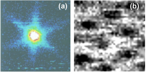
In -wave BCS superconductors the anisotropic order parameter leads to a fourfold anisotropy of the low-energy LDOS around vortices. The LDOS is larger in the direction of the nodes where the spatial decay of the core states is slower Morita et al. (1997a); Franz and Tešanović (1998). In the microscopic Bogoliubov-de Gennes calculations this LDOS anisotropy is weak, but can be as large as close to the core center Morita et al. (1997a); Berthod and Giovannini (2001), and should be accessible experimentally in clean samples. The Eilenberger formalism leads to a more complex and somewhat stronger fourfold anisotropy Schopohl and Maki (1995); Ichioka et al. (1996). Both semiclassical Franz and Tešanović (1999) and microscopic Berthod and Giovannini (2001) calculations showed that self-energy effects can reduce the anisotropy considerably. Although the scope and conclusions of these studies differ, a common prediction is that a weak but characteristic fourfold LDOS anisotropy around vortices should be observed in the conductance maps of -wave superconductors. Up to now, such an observation has never been firmly reported by STS in high- cuprates. There could be several reasons for this. The effect is expectedly very weak, the fourfold features being only a slight deviation from a completely isotropic signal. Then, in case of mixed-symmetry models (e.g. Franz and Tešanović (1998)), the additional components may damp the fourfold character of the spectroscopic signatures. Added to this comes the fact that the coherence length in HTS is extremely short: in Y123 the spectra turn back to be superconducting over a distance of 6–8 nm (Fig. 44a), while in Bi2212 this distance drops to less than 2 nm (Fig. 47a), suggesting that for this material is 3 to 4 times smaller than in Y123. Kugler (2000) performed a quantitative fit of the zero-bias conductance profile across a vortex core, within the framework of a -wave symmetry model Franz and Tešanović (1999). The fitting parameters lead to a value for of the order of 1 nm. These short characteristic lengths imply stringent experimental requirements on spatial resolution, and make the electronic signatures very sensitive to inhomogeneities. Accurate analysis of the conductance images have been performed for both Y123 and Bi2212. Although certain vortices mapped by STS appear with a square shape, the observations report mostly irregular patterns Hoogenboom et al. (2000a). For Bi2212, the cores present no apparent specific symmetry. For Y123, the cores show an overall elliptical shape (Fig. 51b) attributed to the -plane anisotropy of the carrier effective mass (Sec. VII.1.2). The observation of the weak LDOS anisotropy around the vortex cores remains a considerable challenge for future STS studies. It largely depends on the availability of samples with an extremely high degree of homogeneity.
VII.3.2 Irregular shapes of vortices in Bi2212
In Bi2212, images reveal that the vortices often present very irregular shapes, and are in some cases even split into several subcomponents, as shown in Fig. 52a Hoogenboom et al. (2000a). The full pattern (in black in the zero-bias conductance map) extends over an area of about 25 nm2, and in this particular case three subcomponents separated by about 3 nm each can be distinguished. As seen in the spectroscopic trace shown in Fig. 52b, in between these core elements, the spectra turn back to the full superconducting characteristics.
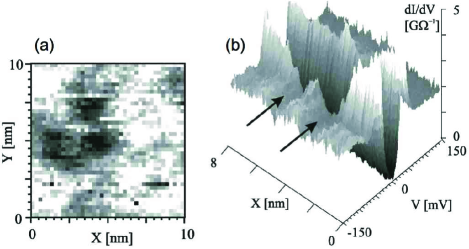
The possibility of vortices occupying neighboring sites may be ruled out for two reasons. Since the expected distance between the vortices at 6 T is of the order of 20 nm, a considerable energy would have to be spent to place the flux lines only 3 nm apart. Moreover, images showing a large number of flux lines ensure that a pattern like the one observed in Fig. 52a is accounting for only one vortex, and that the small subcomponents must belong to the same flux line. The irregular shape of the vortex cores certainly results from doping inhomogeneities. The latter are currently the subject of an intense debate concerning the role they play in the fine electronic structure of HTS (see Sec. V). Since is so small in Bi2212 the superconductor adapts to these inhomogeneities even at short length scales.
The results reported by Hoogenboom et al. (2000a) were interpreted as follows. Fig. 52a would correspond to a situation where a vortex hops back and forth between three pinning sites. This could be either thermally activated motion or quantum tunneling of vortices. Estimates of the tunneling barriers calculated from the positions of the sub-components combined with measurements at 4.2 K and 2.5 K gave evidence for the quantum tunneling scenario. Measurements at lower temperatures have to be carried out in order to reach definitive conclusions. Hoogenboom et al. did also observe a slow shift of weight between the different substructures as a function of time, and concluded that the vortex creep proceeds by this mode rather than by a slow motion of the vortices themselves.
It should be pointed out that the vortex core subcomponents presented in this section are different and should be distinguished from the electronic modulations seen by Hoffman et al. (2002a) and Levy et al. (2005) in the vortex core. In the case of the core subcomponents presented above, the sizes of the structures and the distances separating them are larger. Moreover, the conductance spectra acquired in between these components present the full superconducting characteristics. The electronic modulations are spatial periodic variations in the low-energy part of the conductance spectra, all being observed within the pseudogap spectra characteristic of one single vortex core. That point will be discussed in more details in Sec. VIII.3.
VII.4 Field dependence of the spectra
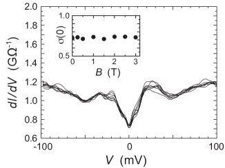
Although STS is not sensitive to the phase of the order parameter, it can reveal electronic features which are a direct consequence of the order parameter symmetry. In the case of the -wave symmetry, the presence of nodes in the gap function gives rise to low-energy nodal quasiparticles with a linear DOS at the Fermi energy (see a critical discussion in Hussey (2002)). With a magnetic field applied parallel to the direction, the superfluid screening currents flow within the planes around the vortices with a velocity . Volovik (1993) suggested that the superfluid velocity would locally shift the quasiparticle energies by an amount , the so-called Doppler shift. He showed that this leads to a behavior of the LDOS outside the core, and to an increase of the zero-energy total DOS proportional to . This behavior of the total DOS was also found in the microscopic calculations Wang and MacDonald (1995). Up to now, the only known possible experimental confirmation of this prediction was provided by specific heat measurements on optimally-doped Y123, by Moler et al. (1994), who found that the magnetic field dependence followed quite precisely the law. In principle, this effect should also be directly measurable by tunneling spectroscopy, through integration of the zero-bias LDOS over the unit cell of the vortex lattice. In Bi2212, the conductance spectra acquired at zero field are similar to the ones acquired at 6 T in between the vortex cores, with no noticeable evolution of the zero-bias conductance. The zero-bias conductance has also been locally measured in optimally-doped Y123 by Maggio-Aprile et al. (1995), and appeared to be field independent up to 3 T (Fig. 53). However, since Y123 presents spectra with a large zero-bias conductance, it is not clear yet whether this observation is reflecting an intrinsic property, or whether other competing factors mask the predicted LDOS behavior, like for instance lifetime effects which may wash out the behavior responsible for the Doppler effect. Franz and Tešanović (1999) also argued that an anisotropic matrix element could lead to a measured tunneling conductance , thus hiding the LDOS behavior. All these factors may explain why the observation of the Volovik effect by STS is challenging.
VII.5 Summary
The possibility to detect vortices with nanometer-scale resolution in HTS is a considerable success, allowing to uncover properties inaccessible to other techniques. Overcoming the problems due to the sample surface quality and homogeneity, individual vortices were probed in both Y123 and Bi2212. For Y123, at high fields and low temperatures, vortices are arranged in an oblique lattice, whose anisotropy is consistent with the observed intrinsic anisotropy of the cores. The direct observation of a twin boundary evidenced its ability to block the perpendicular flux line motion.
For Bi2212, the tiny size of the cores reveals the very small coherence length of this material. The observation of a mostly disordered lattice underlines the strong pinning effect due to defects or inhomogeneities. The latter are also believed to be at the origin of the irregular shapes of the cores. Evidence for quantum tunneling of vortices between close pinning sites has been reported.
For both compounds, the vortex cores revealed striking electronic signatures, which can not be understood within the framework of a conventional BCS -wave or -wave theory. In both underdoped and overdoped Bi2212, the core reveal pseudogap-like spectra, similar to those measured above . A pair of states at finite energy in the vortex cores is systematically observed for both Y123 and Bi2212. Furthermore, the energy of these states scales linearly with the superconducting gap, strongly suggesting that the states for both materials have a common origin.
VIII Local electronic modulations observed by STM
The unusual properties of high-temperature superconductors and the existence of a pseudogap has led to numerous theoretical predictions for the superconducting state as well as the pseudogap state. Some of these imply the existence of spatial charge modulations, either static or dynamic, like stripes, charge density waves, etc. The STM can in principle resolve such charge density variations if they are static or possibly slowly fluctuating, and this has led to a search for such spatial structures in STM topographs or in STS surface maps on Bi2Sr2CaCu2O8+δ. Two different types of spatial variations have been seen by STS: (i) large but irregular spatial variations of the gap, with typical lengths scales of the order of 3–10 nm, in samples which are not specially treated for homogeneity, and (ii) weaker but spatially periodic LDOS modulations with a wavelength of about 1.6–2 nm. The first type of spatial variations are discussed in Sec. V, whereas the periodic modulations appear as a very different phenomenon and are the topic of this section.
The first indication of the presence of such periodic spatial modulations was the observation that around the center of a vortex there is a modulation of the LDOS with a periodicity of about Hoffman et al. (2002a). Subsequently, Howald et al. (2003a) found that charge modulations were also present in the absence of a magnetic field. They reported that the structure appeared at an energy around 25 meV, and that the super-period did not disperse with energy. Hoffman et al. (2002b) reported similar zero-field electronic modulations but in contrast to Howald et al. (2003a), they found that these modulations disperse with energy. They successfully interpreted their findings in terms of quasiparticle interference due to scattering from impurities and other inhomogeneities. More recently Vershinin et al. (2004a) observed electronic modulations in the pseudogap phase above . Contrary to the case of quasiparticle interference patterns, where a large number of vectors were observed, here a single square pattern was detected with a vector that does not disperse with energy. This finding has to be contrasted with the results obtained by McElroy et al. (2005a). They observed at low temperature, in regions of strong underdoping where the coherence peaks in the STS spectra have disappeared, that a non-dispersing square pattern is found at high energy with a period similar to the one seen in the pseudogap phase. A non-dispersing square lattice was subsequently found at low temperature by Hanaguri et al. (2004) in strongly underdoped Ca1-xNaxCuO2Cl2 (NCCOC). Finally, Levy et al. (2005) have recently studied the electronic modulations inside the vortex core in detail. They confirmed the initial observation by Hoffman et al. (2002a), but showed that this modulation does not disperse with energy and thus appears to be similar to the one found in the pseudogap phase. They were also able to link the local square modulation to the localized state structure observed in the vortex core spectra Maggio-Aprile et al. (1995); Pan et al. (2000a); Hoogenboom et al. (2000b). They thus demonstrated the existence of a direct relation between the superconducting state and the vortex-core electronic modulations.
In the following sections we shall first review the electronic modulations resulting from the quasiparticle interference. This will be followed by a discussion of the square pattern in the pseudogap state and of the electronic modulations observed in the vortex cores. Finally we shall discuss the relations between these different findings.
VIII.1 Quasiparticle interference oscillations in the superconducting state
The detection of electronic modulations in the superconducting state is made difficult by the strong tendency of these materials to show inhomogeneities masking the weak periodic modulations. In order to overcome this difficulty Hoffman et al. (2002b) and Howald et al. (2003a) made large maps of the conductance at a given energy. These maps were then Fourier transformed to search for other periodicities than the atomic lattice and the well-known supermodulation in the direction. In Fig. 54 we display such a map and the Fourier transform for different energies. Fig. 54a shows the topography and Fig. 54b the conductance map of the same area at mV. Figs. 54c and d show the Fourier transform of such conductance maps for two different energies.
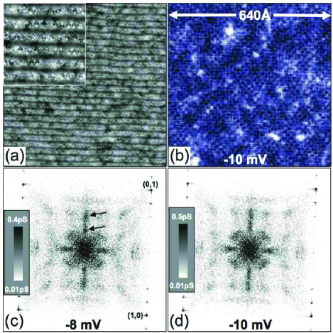
As can easily be seen, in addition to the fine points at high values reflecting the atomic lattice and the super modulation in the direction, one observes a number of more diffuse spots at lower -values reflecting periodic modulations of the local density of states. These spots evolve with energy in a characteristic way. Whereas the -values for the spots in the and directions decrease with increasing energy, the -values for the spots in the directions increase with increasing energy. This can be understood in the framework of quasiparticle interference of a -wave superconductor Hoffman et al. (2002b); Wang and Lee (2003); Zhang and Ting (2003); McElroy et al. (2003). Fig. 55 illustrates the gap variation at the Fermi surface of a -wave superconductor. At a given energy above or below the Fermi energy, interference through potential scattering can occur between points at the Fermi surface linked by the vectors or . This will give rise to oscillations in the LDOS with wave vectors and corresponding to the eight spots discussed above. One sees easily that the length of will decrease with increasing energy (from the Fermi level) and the vector will increase with increasing energy exactly as observed in the experiment.
A more detailed analysis of these results was carried out by McElroy et al. (2003). By using the simple relations between the vectors and the wave vectors one can calculate the locus of the Fermi surface. The result reported by McElroy et al. (2003) is shown in Fig. 56a with a comparison of the ARPES results for the Fermi surface. A striking correspondence is found reinforcing the interpretation that these LDOS oscillations result from quasiparticle interference. Thus, although STM on homogeneous samples does not have -space resolution, this can be obtained when local scattering potentials are introduced, producing quasiparticle interference. The relation can also be deduced from these results as illustrated in Fig. 56b, and compares well to the results reported from ARPES measurements. Such quasiparticle interference oscillations in the LDOS at low temperature were also reported by Vershinin et al. (2004a) on a Bi2212 sample containing 0.6% of Zn impurities. It is important to stress that this quasiparticle interference interpretation of the results implies that there is a sufficient amount of scattering centers in the sample, i.e. that the sample either contains impurities, put in on purpose, or other imperfections resulting from the sample preparation. Thus the intensity of the reflection spots in the Fourier transform is necessarily sample dependent. This may explain why Levy et al. (2005) did not observe such quasiparticle interference patterns in relatively homogeneous samples although they observed the square modulations in the vortex cores.
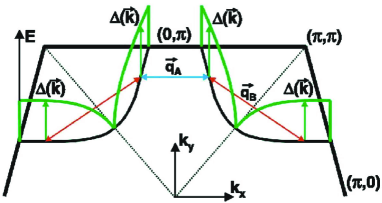
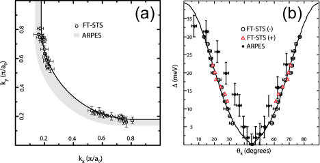
The initial observations of Howald et al. (2003a) contrast with those of Hoffman et al. (2002b) and Vershinin et al. (2004a) in that the dominant features in the Fourier transform are four spots in the Cu-O bond direction. These do not disperse with energy and correspond to an oscillation with a period of about . Howald et al. (2003a) conclude that these spots are there in addition to the spots reflecting the quasiparticle interference. Using a filtered inverse Fourier transform of their images they claim to see evidence for one dimensional stripe-like patterns.
VIII.2 Electronic modulations in the pseudogap state
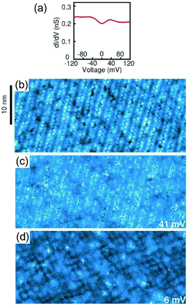
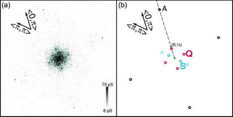
As discussed in Sec. VI the pseudogap state is still not understood. In a recent experiment on a slightly underdoped sample Vershinin et al. (2004a) succeeded to obtain detailed conductance maps at temperatures above and thus to explore the pseudogap state (Fig. 57). The striking result of this investigation is the observation of a square superstructure with -values equal to . As the energy is lowered below the pseudogap one sees a square like disordered pattern appearing. The Fourier transform of one such map is shown in Fig. 58a and illustrated in Fig. 58b. Four spots in the and directions are seen in addition to the spots reflecting the atomic lattice. The intensity of these peaks is energy dependent and they are best seen at low energy around and below 20 meV as illustrated in Fig. 57c,d. On the other hand the positions of these spots in -space do not vary with energy, in contrast to the quasiparticle interference seen at lower temperature in the superconducting state at the same energies. In a more detailed analysis of these results Misra et al. (2004) demonstrated that the results of Vershinin et al. (2004a) cannot be understood in terms of a quasiparticle interference scheme.
Another situation related to the pseudogap was investigated by McElroy et al. (2005a). They studied samples with a strong inhomogeneity in the gap distribution at low temperature, presumably resulting from a local variation in the doping (see Sec. V.4). The larger the gap, i.e. the lower the doping, the smaller are the coherence peaks. Typical spectra from such a sample are shown in Fig. 16c. Selecting strongly underdoped (in average) samples they find large regions where the coherence peaks are completely suppressed. The spectra seen in such regions are illustrated in Fig. 33a together with spectra in higher doping regions with smaller gaps and well developed coherence peaks. They assigned the regions without coherence peaks to a pseudogap behavior and they studied the spatial variations of the local density of states in these regions by suppressing the other regions from the conductance maps. The result is that at low energy they find the same quasiparticle interference patterns as in the regions where a coherence peak is seen. However, in contrast to the latter regions they find at higher energy, above 65 meV, a square pattern similar to the one seen by Vershinin et al. (2004a) in the pseudogap state. This is illustrated in Fig. 59. Their conclusion is that this square pattern, seen at high energy, is a different phenomenon than the quasiparticle oscillations seen at lower energy. Comparing the two reports discussed here Vershinin et al. (2004a); McElroy et al. (2005a), we note the following: the non-dispersing square pattern observed in the pseudogap phase above in a nearly optimally-doped sample is strongest at low energies. On the other hand, in the strongly underdoped samples investigated at low temperature an apparently different behavior is found. Here a non-dispersing pattern is found at high energy while a dispersing quasiparticle interference pattern is found at low energy. We are going to discuss this question further below in Sec. VIII.4.
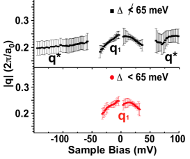
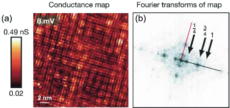
In order to study the pseudogap state in strongly underdoped samples Hanaguri et al. (2004) investigated Ca1-xNaxCuO2Cl2 (NCCOC). The parent compound CaCuO2Cl2 is a Mott insulator and doping with Na makes it a superconductor for . The three compositions studied in this paper all showed a pseudogap-like tunneling spectrum. Conductivity maps at various energies showed a striking electronic order with a dominant superstructure similar to the one seen at high temperature in the pseudogap state in Bi2212. Fig. 60 shows these modulations and their Fourier transform at 8 meV. The characteristic periods are energy independent, as found by Vershinin et al. (2004a) in the pseudogap state above in Bi2212. Another result implicit in the study on NCCOC is that the order appears to be independent of doping. However, since the spectra show no signature of superconductivity, no information about the precise doping level at the surface was given. Another striking result of this study was the observation of additional periodicities inside the unit cell. A structure was also found, suggesting a non commensurate electronic modulation and thus a more complex structure than observed by Vershinin et al. (2004a). Very recently, Momono et al. (2005) studied two different surfaces of Bi2212 at low temperature, one (A) showing pseudogap tunneling spectra and the other (B) superconducting spectra with coherence peaks. Surface A showed a well-developed type non-dispersive modulation, whereas surface B did not show this modulation except for a small area.
VIII.3 Electronic modulations in the vortex core
Hoffman et al. (2002a) analyzed conductance maps of Bi2212 taken in the presence of a magnetic field. These maps were obtained by plotting the differential conductance integrated between 0 and 12 meV. Because of the inhomogeneity of their samples they measured also the maps in zero field and obtained a difference map by subtracting the latter from the former. This is a delicate and difficult operation, but has the advantage that much of the perturbations due to inhomogeneities are eliminated. In this way they were able to show that the local density of states has a spatial modulation in the vortex core. In Fig. 61 we display such a difference map showing a few “lattice points” per vortex due to this local order. Note that the variation in the conductance is of the order of 10% of the zero-field signal.
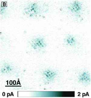
More recently Levy et al. (2005) have carried out a detailed study of the behavior of an individual vortex in Bi2212. Fig. 47a shows a vortex imaged at meV as well as the spectra taken just outside the vortex and close to the vortex center. The salient features of the spectrum close to the center is that one sees a large gap-like structure reflecting the pseudogap as discussed in Secs. VI and VII, and two peaks placed at suggesting the presence of one pair of localized states. Two questions motivated the investigations: (i) How does the square pattern observed in the vortex cores relate to the square pattern observed in the pseudogap state above ? (ii) How does this square pattern in the vortex core relate to the localized state?
When this vortex was imaged at the energy of the core state (Fig. 62a) a square pattern oriented in the Cu-O bond direction was obtained at the center of the vortex. The Fourier transform of this pattern (Fig. 62b) showed, in addition to the atomic lattice, four spots with a period close to . A filtered inverse Fourier transform, selecting an area including the four spots, illustrates the correspondence between the latter and the pattern seen in the 6 meV image (Fig. 62c). The dominant square pattern in Fig. 62a is well reproduced in Fig. 62c. Note the difference in scale between Fig. 62a and Fig. 61. The individual spots inside each vortex of the latter correspond to the large spots in Figs. 62a. The fine structures in Fig. 62a show the atomic lattice on which is superposed the period in one spatial direction.
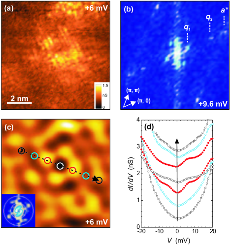
Since it has been found that the vortex-core spectra show the pseudogap (Sec. VI.2.1) one might expect that the spatially ordered structure in the vortex cores has the same origin as the one observed in the pseudogap state. One important property of the spatial modulations in the pseudogap, as discussed in Sec. VIII.2, is the absence of dispersion of the vectors, contrary to the modulations observed in the low-temperature superconducting state. Thus one criterion in comparing the vortex cores with the pseudogap is to check whether the observed order disperses or not. This was also studied by Levy et al. (2005), who plotted the intensity of the Fourier transform along the direction for different energies. The position of the local order was indeed found to be independent of energy, exactly as observed for the pseudogap. The period in this overdoped sample was , somewhat less than observed in the underdoped sample by Vershinin et al. (2004a). This difference could be due either to a difference in doping or to the difference in temperature. Note that in the direction Levy et al. (2005) also observed the modulation seen in NCCOC by Hanaguri et al. (2004).
The relation to the localized states was also studied by Levy et al. (2005) who demonstrated that the intensity of the peaks corresponding to these states is maximal at the four spots reflecting the local order, whereas in between and outside these four spots the peaks at are absent (Fig. 62d). Since the spatial dependence of the peaks (no dispersion with position) suggests that these two peaks reflect only one pair of localized states (see Sec. VII.2), the STS measures the square of the wave function of this state. Thus the four spot pattern in the center of the vortex may be understood as a plot of the wave function of the localized state. Note that this pattern is very different from what one would obtain for a classical -wave localized state as predicted by Caroli et al. (1964).
VIII.4 Discussion
In this section we have discussed some of the striking recent scanning tunneling spectroscopy observations on high-temperature superconductors. A detailed analysis of the tunneling spectra taken with high spatial resolution over large areas has revealed periodic variations with a spatial wavelength of the order of 4–5. These variations correspond to small, sometimes very small, spatial changes of the tunneling spectra. This has to be distinguished from the large gap inhomogeneities often found in these crystals as discussed in Sec. V.
The observed phenomena can be divided into two classes: (i) the modulations with dispersing wave lengths and (ii) the ones which do not disperse or have a much weaker dispersion than the former. The first category is observed in the superconducting state by two groups. These modulations are characterized by a large number of points in the Fourier transform and the position of these points disperse in a characteristic way with energy. In a series of papers, Wang and Lee (2003); Zhang and Ting (2003); McElroy et al. (2003); Hoffman et al. (2002b) interpreted convincingly these structures as modulations due to quasiparticle interference resulting from scattering on impurities and other imperfections. Note that with the observed behavior this explanation can only work if we have a -wave superconductor. An -wave superconductor would not give the same pattern. Also, the intensity of such charge modulations must depend on the amount of scattering centers in the sample and thus depends on the quality of the sample. This may explain why in some cases this type of density of states modulations have not been observed Levy et al. (2005). From these results one can determine the band structure around the Fermi surface as well as the angular dependence of the gap. These data, which agree largely with the results from ARPES, demonstrate beautifully how the STM, in addition to its spatial resolution also can have -space resolution.
The second category of spatial modulations have so far been observed in the pseudogap state either at high temperature, at low doping, or in the vortex cores. In one case Howald et al. (2003a) such modulations were reported in a Bi2212 sample which was inhomogeneous but on the average superconducting. In another case Momono et al. (2005) weak signs of modulations were observed on a superconducting surface, but modulations appeared strongly on a surface showing pseudogap behavior. In yet another case this was reported on NCCOC samples which were nominally superconducting but whose surfaces showed dominantly pseudogap-like spectra. Comparing all these data, there is considerable evidence that the non-dispersing order appears when -wave superconductivity is suppressed, thus that this order is a characteristic behavior of the pseudogap state. In addition to the absence of dispersion, all these square lattices have similar periodicities and the same orientation with respect to the atomic lattice. The reported periods are in the pseudogap above in an underdoped Bi2212 sample Vershinin et al. (2004a), in the vortex cores at low temperature in a slightly overdoped Bi2212 sample Levy et al. (2005) and at low temperature in a strongly underdoped oxychloride Hanaguri et al. (2004). A possible common interpretation of these numbers is that the square local ordering occurs at at low doping and that the period increases with doping and temperature.
The observation of McElroy et al. (2005a) that the square pattern is seen at high energies in strongly underdoped samples and that in the same samples the dispersing quasiparticle interference pattern is seen at low energies seem at first to be contrary to the above conclusions. However, in this experiment the authors studied strongly underdoped regions in an inhomogeneous sample. In these regions superconducting coherence seems to be lost at high energy, i.e. for states around but present at low energy, i.e. around . In this sense the sample is partly in the superconducting state and partly in a pseudogap state. Thus depending on the energy one observes quasiparticle interference, characteristic of a superconducting state, or a square pattern characteristic of a pseudogap.
The experiments on the vortex cores by Levy et al. (2005) bring a new dimension into this picture. The square pattern observed in the vortex core represents the spatial distribution of the localized state. On the other hand this pattern is very similar to the order found in the pseudogap state: both do not disperse and both have a maximum amplitude at low energy below 20 meV. Furthermore, the overall spectra of the pseudogap state and the vortex core have been shown to be the same. This raises the question about the precise relation between the localized state and the square pattern and in particular the question if the so-called localized state is also a characteristics of the pseudogap phase. So far no signature of a state at has been observed in the pseudogap above , but such a structure would most probably be thermally smeared so that one would not see it at temperatures of the order of 100 K. Thus it remains a challenge to determine whether or not there is such a state related to the zero-field pseudogap. Another scenario is that the square pattern is the characteristic feature of the pseudogap, and that the localized state develops in the vortex core thanks to the presence of the square pattern.
The recent STM observations reviewed here, either in the heavily underdoped NCCOC at low temperature, in the slightly underdoped Bi2212 above , or in the vortex cores of slightly overdoped Bi2212, consistently reveal a tendency towards local electronic ordering when the -wave superconductivity is suppressed and the pseudogap is formed. The relation between the superconducting state and the pseudogap state, and the appearance of spatial ordering, have been the origin of numerous papers and discussions.191919See e.g. Zaanen and Gunnarsson (1989); Zhang (1997); Emery and Kivelson (1999); Vojta and Sachdev (1999); Wen and Lee (1996); Chakravarty et al. (2001). Several theories have predicted that the pseudogap corresponds to an ordered state. One-dimensional charge modulations, stripes, could be one candidate. Howald et al. (2003a) argue that their observations show evidence for one-dimensional stripes. However, subsequent observations all show a clear two-dimensional pattern. One possible way out within this scenario would be that the two-dimensional pattern result from fluctuating one-dimensional domains, or that the two-dimensional order result from the observation of two CuO2 planes with crossed one-dimensional orders as put forward by Fine (2004). However, there is at present, with the exception of Howald et al. (2003a), no experimental STM evidence in favor of any of those scenarios. Another possibility would be that the local ordering is due to a spin-density wave (SDW) pinned by vortices. The SDW has been attributed to the proximity of a quantum phase transition Demler et al. (2001); Zhang et al. (2002) or to strong quantum phase fluctuations Franz et al. (2002). Neutron scattering experiments have given ample evidence for the presence of such fluctuations Cheong et al. (1991); Lake et al. (1999). If such fluctuations are pinned by imperfections a modulation in the LDOS may result. It has also been argued that there is a local anti-ferromagnetic order in the vortex cores Zhang (1997); Arovas et al. (1997); Zhu et al. (2002); Takigawa et al. (2004) which may be reflected in the local ordering observed in STM. Several other possibilities remain as to the nature of this electronic order. Conventional charge-density waves Vojta (2002) seem inconsistent with the data: this type of order, as well as charged stripes discussed above, would induce LDOS modulations which are approximately odd with respect to the bias polarity Podolsky et al. (2003); Chen et al. (2004). In these scenarios one would also not understand why the gaps in the LDOS are always pinned at the Fermi energy Franz (2004). Other types of order involve the doped holes themselves. Using a variational approach to study a generalized Hubbard model, Fu et al. (2004) found an insulating ground state at doping , made of square-ordered solitons on top of an anti-ferromagnetic background. They argued that additional holes would make this system metallic and eventually superconducting at higher doping levels. The existence of this state was questioned by White and Scalapino (2004), who found that this type of structures are unstable in the - model; instead, they suggested that pinned CDW along the one-dimensional stripes would lead to patterns similar to the ones observed experimentally.
One important experimental finding brought about by the STM investigations is a strong evidence that the superconducting state, the pseudogap state and the local square order have a common origin. Emery et al. (1997) proposed that the pseudogap reflects fluctuating superconductivity with pair correlations persisting well above . A possible scenario within this scheme would be that in the pseudogap state pairs localize and form a disordered static lattice which can be seen in STM only below the pairforming energy, i.e. the pseudogap. Several authors have proposed that the LDOS modulations reflect the spatial ordering of hole pairs rather than single holes Chen et al. (2002); Anderson (2004); Tešanović (2004); Melikyan and Tešanović (2005).
The new findings by STM reported in this section clearly shine new light on the quest for an understanding of the microscopic nature of both the superconducting state and the pseudogap state. Further investigations along these lines will certainly be necessary to unravel the detailed mechanisms behind the relation between the two phenomena.
IX Conclusion
Over the last decade scanning tunneling spectroscopy has evolved into a major experimental tool in the quest for an understanding of the high-temperature superconductors. The first main achievement of STS on HTS was to bring tunneling experiments into focus again after the first tunneling experiments on high-temperature superconductors using various methods failed to give reproducible results. In fact, studying the spatial dependence it was possible to demonstrate reproducible and homogeneous tunneling on high-quality Bi2212 samples Renner and Fischer (1994a, 1995). It thus became clear that the tunneling spectra were consistent with -wave symmetry, but with an unusual high value of the gap. Later on, other groups stressed the fact that samples often are inhomogeneous Howald et al. (2001); Pan et al. (2001) even if other measurements tend to indicate higher homogeneity. Thus, STS with its very high spatial resolution revealed an inhomogeneity that was not fully recognized by other methods.
STS has led to a number of important discoveries. In 1995 the vortex cores could be imaged on Y123 and anomalous vortex-core spectra were observed Maggio-Aprile et al. (1995), very different from expectations of the BCS theory (-wave or -wave). In 1998 the pseudogap was observed in Bi2212 by STM both in underdoped and overdoped samples Renner et al. (1998a). Prior to that the pseudogap was believed to be only present in underdoped samples. STS has also uncovered the striking doping dependence of the density of states, including the doping dependence of the gap and the pseudogap and their scaling relations. It was recognized that the pseudogap phase is present in the vortex cores at low temperature Renner et al. (1998b). Pan et al. (2000a) and Hoogenboom et al. (2000b) found later that weak signals from localized states are also present in the vortex cores in Bi2212. Hoogenboom et al. (2001) showed that the localized states in Bi2212 and Y123 both follow a universal linear scaling with the superconducting gap and thus that the vortex-core structures in Y123 and Bi2212 have the same origin. Two groups reported spectroscopic studies of impurities in Bi2212 and showed that a zero-bias resonance appears at the site of a non-magnetic impurity, as expected for a -wave superconductor Yazdani et al. (1999); Hudson et al. (1999). The introduction of Fourier transformed conductance maps opened new possibilities Hoffman et al. (2002b); Howald et al. (2003a). This led to the discovery of periodic modulations of the local density of states in the superconducting phase Hoffman et al. (2002b); Howald et al. (2003a) as well as in the pseudogap phase Vershinin et al. (2004a), and in strongly underdoped NCCOC at low temperature Hanaguri et al. (2004). Whereas the modulations in the superconducting state can be understood in terms of quasiparticle interference, the simple square pattern observed in the pseudogap may turn out to be a characteristic signature of order in this phase. The observation of such patterns in the vortex cores by Hoffman et al. (2002a) was recently confirmed by Levy et al. (2005) who demonstrated the close relations between the localized states and the square pattern. These and other results reported in this review have uncovered a large number of remarkable and unexpected behaviors of the high-temperature superconductors. The STM/STS studies have thus made essential contributions to our understanding of high-temperature superconductivity.
Acknowledgments
We thank the current and former members of the Geneva STM group for their contributions to experiments, to discussions, and for their comments: P.-E. Bisson, J.-G. Bosch, J. Cancino, C. Dubois, M. R. Eskildsen, B. W. Hoogenboom, A. D. Kent, G. Levy, A. A. Manuel, Ph. Niedermann, L. Stark. Over the years, we have benefited from numerous scientific discussions with P. Aebi, G. Aeppli, H. Alloul, O. K. Andersen, P. W. Anderson, Y. Ando, A. V. Balatsky, B. Barbiellini, M. R. Beasley, H. Beck, L. Benfatto, G. Blatter, J. C. Campuzano, T. Claeson, P. Coleman, J. C. Davis, D. Dessau, G. Deutscher, A. Erb, T. Feher, L. Forro, M. Franz, H. Fukuyama, T. H. Geballe, T. Giamarchi, E. Giannini, B. Giovannini, W. Hanke, T. Jarlborg, A. Junod, K. Kadowaki, A. Kapitulnik, H. Keller, J. W. Loram, K. Maki, D. van der Marel, P. Martinoli, J. Mesot, V. Mikheev, A. J. Millis, N. Momono, C. de Morais Smith, K. A. Müller, M. R. Norman, S. H. Pan, M. Peter, M. Randeria, T. M. Rice, D. Roditchev, C. Rossel, S. Sachdev, D. J. Scalapino, T. Schneider, S. G. Sharapov, Z.-X. Shen, M. Sigrist, J. L. Tallon, Y. Tanaka, Z. Tešanović, J.-M. Triscone, C. M. Varma, A. Yazdani, A. Yurgens, J. Zaanen, S.-C. Zhang.
We also thank the Swiss National Science Foundation for support through its Divisions II and IV, and through the National Center of Competence in Research MaNEP.
Appendix A The tunneling theory in real space
In this appendix we reproduce the detailed calculation of the single-particle current within the tunneling-Hamiltonian formalism. The derivation follows the procedure given by Mahan (1990); however, we use the real-space formulation of the problem rather than the momentum-space formulation, since our focus is on local probes like the STM.
A.1 Calculation of the tunneling current
The tunnel junction is described by the Hamiltonian
| (11) |
and are the Hamiltonians of the left and right materials, respectively (Fig. 4), which contain all surface and geometric effects such as surface states and defects, surface curvature (e.g. in an STM tip), etc. The central assumption of the model is that the two materials are independent, meaning that the operators on one side of the junction all commute with the operators on the other side, in particular commutes with . The last term in Eq. (11) is the tunneling Hamiltonian, Eq. (2), which is responsible for the transfer of electrons across the junction. It will prove useful to write with
| (12) |
and are the electron creation and destruction operators in the right and left materials, respectively, and gives the probability for an electron to tunnel from a point in the left system to a point in the right system. relates to the the matrix element and the single-particle states of Sec. III through
| (13) |
The tunneling current is simply given by the rate of change of the particle number on the right side Cohen et al. (1962):
| (14) |
Our convention is that and the current is taken positive when the electrons flow from left to right. Since commutes with and we have , in units such that . We now calculate to first order in . The linear-response theory gives
| (15) |
In the r.h.s. of Eq. (15) the time evolution of the operators is governed by , and the angular brackets represent a thermal average with respect to . Since and commute this average factorizes into left and right components. We can therefore assume that the left and right systems are in independent thermodynamic equilibria, and are characterized by two different chemical potentials and . Introducing we rewrite the time evolution of the operator as
| (16) |
where is the applied bias. The last line of Eq. (16) is obtained using and . We then have
| (17a) | |||||
| (17b) | |||||
where the time evolution of and is now governed by as in Eq. (16). Inserting (17) into (15) and using (14) one arrives at the expression
| (18) | |||||
The first term is the single-particle current and the second term is the pair (Josephson) current. According to Eq. (18) is the Fourier transform, at energy , of the retarded correlation function of the (bosonic) operator . The latter is most easily evaluated by analytically continuing onto the real-frequency axis the corresponding temperature propagator (Mahan, 1990, p. 149):
| (19) |
denote the even Matsubara frequencies with the inverse temperature. One thus has
| (20) |
Looking at Eqs. (19) and (12) we see that is made of the terms
| (21) |
We have introduced the temperature Green’s functions on both sides of the junction, with the usual definitions:
| (22a) | |||||
| (22b) | |||||
with the odd Matsubara frequencies. It is then straightforward to evaluate in Eq. (19) using (21) and (22b):
The frequency sum is easily performed within the spectral representation,
| (23) |
and using the usual trick for frequency summation (Mattuck, 1992, p. 251). We have, letting :
Taking the imaginary part, inserting into (20), and reintroducing a dimensional factor , we finally get
| (24) |
Eq. (3) results immediately from Eq. (24) by a change of representation, i.e. substituting the matrix element with Eq. (13) and choosing the single-particle states which diagonalize the spectral function:
General relations about the real-space Green’s function and spectral function are given by Hedin and Lundqvist (1969). Of particular interest is the relation between the spectral function and the local density of states: .
The calculation of the Josephson current proceeds along the same lines, by considering the anomalous correlation function of the operator :
We refer the reader to the work of Josephson (1969) for a detailed discussion of this term.
A.2 STM and the local density of states
Starting from Eq. (24) it is easy to see how the Tersoff and Hamman (1983) matrix element Eq. (8) leads to Eq. (5) for the tunneling current. Inserting into Eq. (13) one gets, owing to the completion property of the functions :
| (25) |
The delta function in the matrix element (25) substitutes in Eq. (24) with . On the other hand, if the tip material is a simple metal its spectral function takes the form Hedin and Lundqvist (1969)
| (26) |
Then the integrals in Eq. (24) cancel the sums of Eq. (25) due to the orthogonality of the functions . Thus Eqs. (24), (25), and (26) lead to
In the calculation of the matrix element Eq. (8), Tersoff and Hamman assumed that the sample electronic structure can be represented by independent electrons, so that was meant as the true wave function in the sample. Nevertheless, we implicitly considered in our derivation that the validity of Eq. (8) carries over to the case where the functions are general basis functions. In this way the validity of Eq. (5) could be extended to correlated systems. We believe that this procedure is correct, since the Tersoff and Hamman calculation does not depend on the detailed form and nature of .
A.3 The case of a non-local matrix element
If the relation between the matrix element and the sample wave function is non-local, like in Eq. (9), then using Eq. (13) the form Eq. (25) is generalized to
| (27) |
The resulting tunneling conductance is, using Eq. (24) and the common approximations for the tip:
| (28) |
If the sample is translation invariant, , this expression takes a simpler form in reciprocal space. Then the conductance no longer depends on and is just Eq. (10).
Appendix B HTS gaps measured by STS
Here we provide a list of superconducting gap values of high- cuprates which have been obtained by scanning tunneling spectroscopy. The superconducting gap is defined by the energy of the superconducting coherence peaks. All collected data where obtained on SIN vacuum tunnel junctions at low temperature and on single crystals with the tip perpendicular to the (001) surface plane (), unless stated differently. The data are listed as a function of increasing doping level for underdoped (UD), optimally-doped (OP), and overdoped (OD) materials.
| (K) | (meV) | Reference | ||
|---|---|---|---|---|
| 0.160 | – | Kugler et al. (Sec. VI.1.2) | ||
| 10b | 0.180 | Kugler et al. (2001) | ||
| 3.5b | 0.185 | Kugler (2000) | ||
| With La or Pb substitutions: | ||||
| 29c | 0.145 | Kugler (2000) | ||
| 10d | – | Mashima et al. (2003) | ||
| a Bi2.2Sr1.8CuO6+δ b Bi2.1Sr1.9CuO6+δ c Bi1.8Sr1.7La0.5CuO6+δ d Bi2.1Pb0.37Sr1.91CuO6+δ | ||||
| (K) | (meV) | Reference | ||
|---|---|---|---|---|
| 63 | (0.10) | 40 | Nakano et al. (1998) | |
| 60 | 0.10 | Oda et al. (1997) | ||
| 65 | 0.11 | 62 | McElroy et al. (2004); McElroy et al. (2005a) | |
| 67 | 0.11 | Matsuda et al. (2003) | ||
| 78 | (0.12) | 50.2 | Hoffman et al. (2002a) | |
| 80 | (0.12) | Howald et al. (2001) | ||
| 81 | (0.12) | 50 | Matsuda et al. (1999b, a) | |
| 81 | (0.12) | 40 | Murakami and Aoki (1995) | |
| 75 | 0.13 | McElroy et al. (2004); McElroy et al. (2005a) | ||
| 86 | (0.13) | 52 | Matsuda et al. (1999b, a) | |
| 83 | (0.13) | Matsuba et al. (2003b) | ||
| (85) | 0.13 | Matsuda et al. (2003) | ||
| 85 | (0.13) | 33 | Nakano et al. (1998) | |
| 83 | (0.13) | 44 | Renner et al. (1998a) | |
| 86 | (0.13) | 45 | Sakata et al. (2003) | |
| 79 | 0.14 | 50 | Lang et al. (2002) | |
| 88 | (0.14) | 50 | Matsuura et al. (1998) | |
| 82 | 0.14 | Oda et al. (1997) | ||
| 79 | 0.15 | McElroy et al. (2004); McElroy et al. (2005a) | ||
| 80 | 0.15 | 38 | Oda et al. (2000) | |
| 92 | (0.16) | 35 | DeWilde et al. (1998) | |
| 92 | (0.16) | 43.7 | Hoffman et al. (2002a) | |
| 92 | [0.16] | Iavarone et al. (1998) | ||
| 84a | [0.16] | 40 | Misra et al. (2002a) | |
| 93ab | (0.16) | – | Cren et al. (2000) | |
| 90 | [0.16] | 54 | Matsuda et al. (1999b, a) | |
| 89 | 0.16 | Matsuda et al. (2003) | ||
| 88 | [0.16] | Oda et al. (1997) | ||
| 92.3 | [0.16] | Renner and Fischer (1995) | ||
| 92.2 | [0.16] | 41.5 | Renner et al. (1998a) | |
| 90 | [0.16] | 39 | Wolf et al. (1994) | |
| 86.5c | (0.18) | Howald et al. (2003a, b) | ||
| 88 | (0.18) | Kitazawa et al. (1997) | ||
| (89) | 0.18 | 35.6 | Lang et al. (2002) | |
| (89) | 0.18 | McElroy et al. (2004); McElroy et al. (2005a) | ||
| (89) | 0.18 | Matsuda et al. (2003) | ||
| 85 | (0.19) | 25 | Chen and Ng (1992) | |
| 85 | (0.19) | 36.7 | Hoffman et al. (2002a) | |
| 87 | (0.19) | 32 | Hudson et al. (1999) | |
| 87 | (0.19) | 26 | Ichimura and Nomura (1993) | |
| 86 | (0.19) | Kaneko et al. (1999) | ||
| 89 | 0.19 | McElroy et al. (2004); McElroy et al. (2005a) | ||
| 85 | (0.19) | 35 | Maki et al. (2001) | |
| 84 | (0.19) | 50 | Matsuda et al. (1999b, a) | |
| 85 | (0.19) | 26 | Nakano et al. (1998) | |
| 84 | (0.19) | 32 | Pan et al. (2000a) | |
| 87 | (0.19) | 17d | Suzuki et al. (1999b) | |
| 87 | (0.19) | – | Suzuki et al. (1999a) | |
| – | – | 40 | – | Hudson et al. (2000) |
| 76.4 | (0.20) | Hoogenboom et al. (2003b) | ||
| 77 | (0.20) | Kugler et al. (2000) | ||
| 77 | (0.20) | Hoogenboom et al. (2000a) | ||
| 77 | (0.20) | Hoogenboom et al. (2000b) | ||
| 80.7 | (0.20) | Hoogenboom et al. (2003b) | ||
| 81 | (0.20) | 43 | Matsuda et al. (1999b, a) | |
| 82 | (0.20) | Oda et al. (1996) | ||
| 72 | (0.21) | 30 | DeWilde et al. (1998) | |
| 72 | (0.21) | Iavarone et al. (1998) | ||
| – | – | – | Mallet et al. (1996) | |
| 81 | 0.21 | Oda et al. (1997) | ||
| 80 | 0.21 | 24 | Oda et al. (2000) | |
| 74.3 | (0.21) | 34 | Renner et al. (1998a) | |
| 74 | (0.21) | Yazdani et al. (1999) | ||
| (64) | 0.22 | Matsuda et al. (2003) | ||
| 56 | (0.23) | 21 | Renner et al. (1998a) | |
| With Zn, Ni, Co or Pb substitutions: | ||||
| 84f | (0.13) | 45 | Pan et al. (2000b) | |
| 85g | (0.19) | 20 | Hudson et al. (2003) | |
| – h | – | 50i | – | Zhao et al. (2000) |
| – j | – | 50 | – | Cren et al. (2001) |
| 68k | (0.22) | Kinoda et al. (2003) | ||
| a Thin film b Bi2Sr1.98Ca1.38Cu2.28O8+δ, K by dc-resistivity and 55 K by ac-susceptibility c Bi2.1Sr1.9CaCu2O8+δ d Tunneling direction in -plane varies between [110] and [100] e f Bi2Sr2Ca(Cu1-xZnx)2O8+δ g Bi2Sr2Ca(Cu1-xNix)2O8+δ h Bi1.83Sr1.8Ca(Cu1-xCox)2O8+δ i Measured at K j Bi1.95Pb0.5Sr2CaCu2O8+δ k Bi1.4Pb0.6Sr2CaCu2O8+δ | ||||
| (K) | (meV) | Reference | ||
|---|---|---|---|---|
| 109 | UD | Kugler et al. (2006) | ||
| 111 | OP | Kugler et al. (2006) | ||
| (K) | (meV) | Reference | ||
|---|---|---|---|---|
| Hg1201 | ||||
| 97a | OP | 33 | Wei et al. (1998a) | |
| Hg1212 | ||||
| 123b | OP | 50 | Wei et al. (1998a) | |
| Hg1223 | ||||
| 125c | (OP) | Rossel et al. (1994) | ||
| 133a | (OP) | Rossel et al. (1994) | ||
| 135a | OP | 75 | Wei et al. (1998a) | |
| a Polycrystal b Thin film c Melted sample d meV using Dynes fit e meV using Dynes fit | ||||
| (K) | (meV) | Reference | ||
|---|---|---|---|---|
| 29.5 | 0.10 | 7.5 | Tanaka et al. (1995, 1996) | |
| 0.14 | 16 | Nakano et al. (1998) | ||
| 0.14 | 17 | Oda et al. (2000) | ||
| 33 | 0.15 | 7 | Kirtley et al. (1987) | |
| 35.5 | 0.15 | 5.5 | Tanaka et al. (1995, 1996) | |
| 39 | 0.16 | Kato et al. (2003) | ||
| 0.18 | 10 | Nakano et al. (1998) | ||
| 0.18 | 9 | Oda et al. (2000) | ||
| (K) | (meV) | Reference | ||
|---|---|---|---|---|
| 60 | UD | Yeh et al. (2001) | ||
| 85a | UD | 19 | Yeh et al. (2001) | |
| 89 | UD | 20 | Born et al. (2002) | |
| 82b | OP | 18 | Yeh et al. (2001) | |
| 85c | (OP) | Kirtley et al. (1987) | ||
| 85c | (OP) | Kirtley et al. (1987) | ||
| 90a | ? | Hoevers et al. (1988) | ||
| 90 | OP | 28f | Tanaka et al. (1994) | |
| 90a | OP | Ueno et al. (2001, 2003) | ||
| 90 | OP | Wan et al. (1989) | ||
| (OP) | Miller et al. (1993) | |||
| 91 | (OP) | – | Murakami et al. (2001) | |
| 91 | (OP) | Murakami et al. (2001) | ||
| 92a | OP | Alff et al. (1997) | ||
| 92a | OP | 20 | Born et al. (2002) | |
| 92 | OP | Edwards et al. (1992) | ||
| 92 | OP | Edwards et al. (1995) | ||
| 92a | OP | Koinuma et al. (1993) | ||
| 92a | OP | Koyanagi et al. (1995) | ||
| 92 | OP | Kugler et al. (2000) | ||
| 92 | OP | Maggio-Aprile et al. (1995) | ||
| 92 | OP | Maggio-Aprile et al. (2000) | ||
| 92 | (OP) | 18 | Maki et al. (2001) | |
| 92a | OP | Nantoh et al. (1994a) | ||
| 92a | OP | Nantoh et al. (1995) | ||
| 92 | OP | Wei et al. (1998b) | ||
| 92 | OP | Wei et al. (1998b) | ||
| 92 | OP | Wei et al. (1998b) | ||
| 92.9 | OP | 18 | Yeh et al. (2001) | |
| 90 | OD | 20 | Shibata et al. (2003a, b) | |
| 78ai | OD | 19 | Yeh et al. (2001) | |
| a Thin film b YBa2Cu0.9934Zn0.0026Mg0.0043O6.9 c Measured by high-field magnetic susceptibility, K by resistivity d -plane e Tunneling on (100) plane f Tunneling on (110) and (100) planes g Tunneling on electrical field etched surface h Tunneling on (110) plane i Y0.7Ca0.3Ba2Cu3O7-δ | ||||
| (K) | (meV) | Reference | ||
|---|---|---|---|---|
| 95a | OP | 30 | Nishiyama et al. (2002) | |
| a Measured by SQUID | ||||
References
- Abrikosov (1957) Abrikosov, A. A., 1957, Sov. Phys.–JETP 5, 1174.
- Abrikosov and Gor’kov (1960) Abrikosov, A. A., and L. P. Gor’kov, 1960, Sov. Phys.–JETP 12, 1243.
- Affleck et al. (1997) Affleck, I., M. Franz, and M. H. Sharifzadef Amin, 1997, Phys. Rev. B 55, R704.
- Affleck and Marston (1988) Affleck, I., and J. B. Marston, 1988, Phys. Rev. B 37, 3774.
- Aleszkiewicz et al. (1997) Aleszkiewicz, M., P. Aleszkiewicz, and J. Rauluszkiewicz, 1997, Czech. J. Phys. 47, 367.
- Alff et al. (2003) Alff, L., Y. Krockenberger, B. Welter, M. Schonecke, R. Gross, D. Manske, and M. Naito, 2003, Nature 422, 698.
- Alff et al. (1998) Alff, L., A. Marx, R. Gross, A. Beck, H. Takashima, S. Kashiwaya, M. Koyanagi, and Y. Tanaka, 1998, Appl. Supercond. 6, 783.
- Alff et al. (1997) Alff, L., H. Takashima, S. Kashiwaya, N. Terada, H. Ihara, Y. Tanaka, M. Koyanagi, and K. Kajimura, 1997, Phys. Rev. B 55, R14757.
- Alloul et al. (1989) Alloul, H., T. Ohno, and P. Mendels, 1989, Phys. Rev. Lett. 63, 1700.
- Anagawa et al. (2003) Anagawa, K., Y. Yamada, T. Watanabe, and M. Suzuki, 2003, Phys. Rev. B 67, 214513.
- Andersen et al. (2000) Andersen, B. M., H. Bruus, and P. Hedegård, 2000, Phys. Rev. B 61, 6298.
- Anderson (1959) Anderson, P. W., 1959, J. Phys. Chem. Solids 11, 26.
- Anderson (1987) Anderson, P. W., 1987, Science 235, 1196.
- Anderson (1997) Anderson, P. W., 1997, The Theory of Superconductivity in the High- Cuprates (Princeton University Press, Princeton).
- Anderson (2004) Anderson, P. W., 2004, eprint cond-mat/0406038.
- Anderson et al. (2004) Anderson, P. W., P. A. Lee, M. Randeria, T. M. Rice, N. Trivedi, and F. C. Zhang, 2004, J. Phys.: Condens. Matter 16, R755.
- Anderson and Ong (2006) Anderson, P. W., and N. P. Ong, 2006, J. Phys. Chem. Solids 67, 1.
- Ando et al. (2000) Ando, Y., Y. Hanaki, S. Ono, K. Segawa, Y. Abe, and N. Miyamoto, 2000, Phys. Rev. B 61, R14956.
- Appelbaum and Brinkman (1969a) Appelbaum, J. A., and W. F. Brinkman, 1969a, Phys. Rev. 183, 553.
- Appelbaum and Brinkman (1969b) Appelbaum, J. A., and W. F. Brinkman, 1969b, Phys. Rev. 186, 464.
- Aprili et al. (1999) Aprili, M., E. Badica, and L. H. Greene, 1999, Phys. Rev. Lett. 83, 4630.
- Aprili et al. (1998) Aprili, M., M. Covington, E. Paraoanu, B. Niedermeier, and L. H. Greene, 1998, Phys. Rev. B 57, R8139.
- Arovas et al. (1997) Arovas, D. P., A. J. Berlinsky, C. Kallin, and S.-C. Zhang, 1997, Phys. Rev. Lett. 79, 2871.
- Balatsky et al. (1995) Balatsky, A. V., M. I. Salkola, and A. Rosengren, 1995, Phys. Rev. B 51, 15547.
- Balatsky et al. (2006) Balatsky, A. V., I. Vekhter, and J.-X. Zhu, 2006, Rev. Mod. Phys. 78, 373.
- Bardeen (1961) Bardeen, J., 1961, Phys. Rev. Lett. 6, 57.
- Bardeen (1962) Bardeen, J., 1962, Phys. Rev. Lett. 9, 147.
- Bardeen et al. (1957) Bardeen, J., L. N. Cooper, and J. R. Schrieffer, 1957, Phys. Rev. 108, 1175.
- Bednorz and Müller (1986) Bednorz, J. G., and K. A. Müller, 1986, Z. Phys. B 64, 189.
- Behler et al. (1994) Behler, S., S. H. Pan, P. Jess, A. Baratoff, H.-J. Guenterodt, F. Levy, G. Wirth, and J. Wiesner, 1994, Phys. Rev. Lett. 72, 1750.
- Berthod and Giovannini (2001) Berthod, C., and B. Giovannini, 2001, Phys. Rev. Lett. 87, 277002.
- Besocke (1987) Besocke, K., 1987, Surf. Sci. 181, 145.
- Beuermann (1981) Beuermann, G., 1981, Z. Phys. B 44, 29.
- Binnig and Rohrer (1982a) Binnig, G., and H. Rohrer, 1982a, Helv. Phys. Acta 55, 726.
- Binnig and Rohrer (1982b) Binnig, G., and H. Rohrer, 1982b, Helv. Phys. Acta 55, 128.
- Binnig and Rohrer (1987) Binnig, G., and H. Rohrer, 1987, Rev. Mod. Phys. 59, 615.
- Biswas et al. (2001) Biswas, A., P. Fournier, V. N. Smolyaninova, R. C. Budhani, J. S. Higgins, and R. L. Greene, 2001, Phys. Rev. B 64, 104519.
- Blonder et al. (1982) Blonder, G. E., M. Tinkham, and T. M. Klapwijk, 1982, Phys. Rev. B 25, 4515.
- Born et al. (2002) Born, V., C. Jooss, and H. C. Freyhardt, 2002, Physica C 382, 224.
- Brown et al. (2004) Brown, S. P., D. Charalambous, E. C. Jones, E. M. Forgan, P. G. Kealey, A. Erb, and J. Kohlbrecher, 2004, Phys. Rev. Lett. 92, 067004.
- Büttiker et al. (1985) Büttiker, M., Y. Imry, R. Landauer, and S. Pinhas, 1985, Phys. Rev. B 31, 6207.
- Byers et al. (1993) Byers, J. M., M. E. Flatté, and S. D. J., 1993, Phys. Rev. Lett. 71, 3363.
- Campuzano et al. (1990) Campuzano, J. C., G. Jennings, M. Faiz, L. Beaulaigue, B. W. Veal, J. Z. Liu, A. P. Paulikas, K. Vandervoort, H. Claus, R. S. List, A. J. Arko, and R. J. Bartlett, 1990, Phys. Rev. Lett. 64, 2308.
- Campuzano et al. (2004) Campuzano, J. C., M. Norman, and M. Randeria, 2004, in Physics of Superconductors, edited by K. H. Bennemann and J. B. Ketterson (Springer), volume II, p. 167.
- Carlson et al. (2004) Carlson, E. W., V. J. Emery, S. A. Kivelson, and D. Orgad, 2004, in The Physics of Superconductors, edited by K. H. Bennemann and J. B. Ketterson (Springer-Verlag), volume II.
- Carminati and Sáenz (2000) Carminati, R., and J. J. Sáenz, 2000, Phys. Rev. Lett. 84, 5156.
- Caroli et al. (1971) Caroli, C., R. Combescot, P. Nozières, and D. Saint-James, 1971, J. Phys. C: Solid State Phys. 4, 916.
- Caroli et al. (1964) Caroli, C., P. G. de Gennes, and J. Matricon, 1964, Phys. Lett. 9, 307.
- Chakravarty et al. (2001) Chakravarty, S., R. B. Laughlin, D. K. Morr, and C. Nayak, 2001, Phys. Rev. B 63, 094503.
- Chakravarty et al. (1993) Chakravarty, S., A. Sudbø, P. W. Anderson, and S. Strong, 1993, Science 261, 337.
- Chen (1988) Chen, C. J., 1988, J. Vac. Sci. Technol. A 6, 319.
- Chen (1990a) Chen, C. J., 1990a, Phys. Rev. Lett. 65, 448.
- Chen (1990b) Chen, C. J., 1990b, Phys. Rev. B 42, 8841.
- Chen (1993) Chen, C. J., 1993, Introduction to Scanning Tunneling Microscopy (Oxford University Press, New-York).
- Chen et al. (2002) Chen, H.-D., J.-P. Hu, S. Capponi, E. Arrigoni, and S.-C. Zhang, 2002, Phys. Rev. Lett. 89, 137004.
- Chen et al. (2004) Chen, H.-D., O. Vafek, A. Yazdani, and S.-C. Zhang, 2004, Phys. Rev. Lett. 93, 187002.
- Chen and Ng (1992) Chen, Q., and K.-W. Ng, 1992, Phys. Rev. B 45, 2569.
- Chen et al. (2005) Chen, Q., J. Stajic, S. Tan, and K. Levin, 2005, Phys. Rep. 412, 1.
- Chen and Lin (2004) Chen, X. J., and H. Q. Lin, 2004, Phys. Rev. B 69, 104518.
- Chen and Ting (2002) Chen, Y., and C. S. Ting, 2002, Phys. Rev. B 65, 180513(R).
- Cheong et al. (1991) Cheong, S. W., G. Aeppli, T. E. Mason, H. Mook, S. M. Hayden, P. C. Canfield, Z. Fisk, K. N. Clausen, and J. L. Martinez, 1991, Phys. Rev. Lett. 67, 1791.
- Chubukov et al. (2003) Chubukov, A. V., D. Pines, and J. Schmalian, 2003, in Conventional and High- Superconductors, edited by K. Bennemann and J. Ketterson (Springer), volume I of The Physics of Superconductors, p. 495.
- Chubukov et al. (1996) Chubukov, A. V., D. Pines, and B. P. Stojković, 1996, J. Phys.: Condens. Matter 8, 10017.
- Ciraci and Batra (1987) Ciraci, S., and I. P. Batra, 1987, Phys. Rev. B 36, 6194.
- Clogston (1962) Clogston, A. M., 1962, Phys. Rev. Lett. 9, 266.
- Cohen et al. (1962) Cohen, M. H., L. M. Falicov, and J. C. Phillips, 1962, Phys. Rev. Lett. 8, 316.
- Coleman et al. (1992) Coleman, R. V., Z. Dai, W. W. McNairy, C. G. Slough, and C. Wang, 1992, in Surface Properties of Layered Structures, edited by G. Benedek (Kluwer Academic), p. 27.
- Crabtree et al. (1996) Crabtree, G. W., G. K. Leaf, H. G. Kaper, V. M. Vinokur, A. E. Koshelev, D. W. Braun, D. M. Levine, W. K. Kwok, and J. A. Fendrich, 1996, Physica C 263, 401.
- Cren et al. (2001) Cren, T., D. Roditchev, W. Sacks, and J. Klein, 2001, Europhys. Lett. 54, 84.
- Cren et al. (2000) Cren, T., D. Roditchev, W. Sacks, K. Klein, J.-B. Moussy, C. Deville-Cavellin, and M. Laguës, 2000, Phys. Rev. Lett. 84, 147.
- Cuevas et al. (1996) Cuevas, J. C., A. Martín-Rodero, and A. Levy Yeyati, 1996, Phys. Rev. B 54, 7366.
- Dagotto (1994) Dagotto, E., 1994, Rev. Mod. Phys. 66, 763.
- Damascelli et al. (2003) Damascelli, A., Z. Hussain, and Z.-X. Shen, 2003, Rev. Mod. Phys. 75, 473.
- Demler et al. (2004) Demler, E., W. Hanke, and S.-C. Zhang, 2004, Rev. Mod. Phys. 76, 909.
- Demler et al. (2001) Demler, E., S. Sachdev, and Y. Zhang, 2001, Phys. Rev. Lett. 87, 067202.
- Derro et al. (2002) Derro, D. J., E. W. Hudson, K. M. Lang, S. H. Pan, J. C. Davis, J. T. Markert, and A. L. de Lozanne, 2002, Phys. Rev. Lett. 88, 097002.
- Dessau et al. (1991) Dessau, D. S., B. O. Wells, Z.-X. Shen, W. E. Spicer, A. J. Arko, R. S. List, D. B. Mitzi, and A. Kapitulnik, 1991, Phys. Rev. Lett. 66, 2160.
- Deutscher (1999) Deutscher, G., 1999, Nature 397, 410.
- Deutscher (2005) Deutscher, G., 2005, Rev. Mod. Phys. 77, 109.
- DeWilde et al. (1997a) DeWilde, Y., M. Iavarone, U. Welp, V. Metlushko, A. E. Koshelev, I. Aranson, G. W. Crabtree, and P. C. Canfield, 1997a, Phys. Rev. Lett. 78, 4273.
- DeWilde et al. (1997b) DeWilde, Y., M. Iavarone, U. Welp, V. Metlushko, A. E. Koshelev, I. Aranson, G. W. Crabtree, P. L. Gammel, D. J. Bishop, and P. C. Canfield, 1997b, Physica C 282-287, 355.
- DeWilde et al. (1998) DeWilde, Y., N. Miyakawa, P. Guptasarma, M. Iavarone, L. Ozyuzer, J. F. Zasadzinski, P. Romano, D. G. Hinks, C. Kendziora, G. W. Crabtree, and K. E. Gray, 1998, Phys. Rev. Lett. 80, 153.
- Ding et al. (1996) Ding, H., T. Yokoya, J. C. Campuzano, T. Takahashi, M. Randeria, M. R. Norman, T. Mochiku, K. Kadowaki, and J. Giapintzakis, 1996, Nature 382, 51.
- Dipasupil et al. (2002) Dipasupil, R. M., M. Oda, and M. Ido, 2002, J. Phys. Soc. Jpn. 71, 1535.
- Dolan et al. (1989a) Dolan, G. J., G. V. Chandrashekhar, T. R. Dinger, C. Feild, and F. Holtzberg, 1989a, Phys. Rev. Lett. 62, 827.
- Dolan et al. (1989b) Dolan, G. J., F. Holtzberg, C. Feild, and T. R. Dinger, 1989b, Phys. Rev. Lett. 62, 2184.
- Doyen et al. (1993) Doyen, G., D. Drakova, and M. Scheffler, 1993, Phys. Rev. B 47, 9778.
- Duke (1969) Duke, C. B., 1969, in Solid State Physics: Advances in Research and Applications, edited by F. Seitz, D. Turnbull, and H. Ehrenreich (Academic Press), volume suppl. 10.
- Eckl et al. (2002) Eckl, T., D. J. Scalapino, E. Arrigoni, and W. Hanke, 2002, Phys. Rev. B 66, 140510.
- Edwards et al. (1995) Edwards, H. L., D. J. Derro, A. L. Barr, J. T. Markert, and A. L. de Lozanne, 1995, Phys. Rev. Lett. 75, 1387.
- Edwards et al. (1992) Edwards, H. L., J. T. Markert, and A. L. de Lozanne, 1992, Phys. Rev. Lett. 69, 2967.
- Edwards et al. (1994) Edwards, H. L., J. T. Markert, and A. L. de Lozanne, 1994, J. Vac. Sci. Technol. B 12, 1886.
- Ekvall et al. (1999) Ekvall, I., E. Wahlström, D. Claesson, H. Olin, and E. Olsson, 1999, Meas. Sci. Technol. 10, 11.
- Eliashberg (1960) Eliashberg, G. M., 1960, Sov. Phys.–JETP 11, 696.
- Emery and Kivelson (1995) Emery, V. J., and S. A. Kivelson, 1995, Nature 374, 434.
- Emery and Kivelson (1999) Emery, V. J., and S. A. Kivelson, 1999, J. Low Temp. Phys. 117, 189.
- Emery et al. (1990) Emery, V. J., S. A. Kivelson, and H. Q. Lin, 1990, Phys. Rev. Lett. 64, 475.
- Emery et al. (1997) Emery, V. J., S. A. Kivelson, and O. Zachar, 1997, Physica C 282, 174.
- Eschrig and Norman (2000) Eschrig, M., and M. R. Norman, 2000, Phys. Rev. Lett. 85, 3261.
- Eskildsen et al. (1997) Eskildsen, M. R., P. L. Gammel, B. P. Barber, A. P. Ramirez, D. J. Bishop, N. H. Andersen, K. Mortensen, C. A. Bolle, C. M. Lieber, and P. C. Canfield, 1997, Phys. Rev. Lett. 79, 487.
- Eskildsen et al. (2002) Eskildsen, M. R., M. Kugler, S. Tanaka, J. Jun, S. M. Kazakov, J. Karpinski, and Ø. Fischer, 2002, Phys. Rev. Lett. 89, 187003.
- Essmann and Träuble (1967) Essmann, U., and H. Träuble, 1967, Phys. Lett. A 24, 526.
- Fang et al. (2004) Fang, A., C. Howald, N. Kaneko, M. Greven, and A. Kapitulnik, 2004, Phys. Rev. B 70, 214514.
- Feng et al. (2000) Feng, D. L., D. H. Lu, K. M. Shen, C. Kim, H. Eisaki, A. Damascelli, R. Yoshizaki, J.-I. Shimoyama, K. Kishio, G. D. Gu, S. Oh, A. Andrus, et al., 2000, Science 289, 277.
- Feuchtwang (1974) Feuchtwang, T. E., 1974, Phys. Rev. B 10, 4121.
- Fine (2004) Fine, B. V., 2004, Phys. Rev. B 70, 224508.
- Foley et al. (2000) Foley, E. T., A. F. Kam, and J. W. Lyding, 2000, Rev. Sci. Instrum. 71,, 3428,.
- Fong et al. (1999) Fong, H. F., P. Bourges, Y. Sidis, L. P. Regnault, A. Ivanov, G. D. Gu, N. Koshizuka, and B. Keimer, 1999, Nature 398, 588.
- Fong et al. (1995) Fong, H. F., B. Keimer, P. W. Anderson, D. Reznik, F. Dogan, and I. A. Aksay, 1995, Phys. Rev. Lett. 75, 316.
- Franz (2004) Franz, M., 2004, Science 305, 1410.
- Franz and Millis (1998) Franz, M., and A. J. Millis, 1998, Phys. Rev. B 58, 14572.
- Franz et al. (2002) Franz, M., D. E. Sheehy, and Z. Tešanović, 2002, Phys. Rev. Lett. 88, 257005.
- Franz and Tešanović (1998) Franz, M., and Z. Tešanović, 1998, Phys. Rev. Lett. 80, 4763.
- Franz and Tešanović (1999) Franz, M., and Z. Tešanović, 1999, Phys. Rev. B 60, 3581.
- Franz and Tešanović (2001) Franz, M., and Z. Tešanović, 2001, Phys. Rev. Lett. 87, 257003.
- Fu et al. (2004) Fu, H. C., J. C. Davis, and D.-H. Lee, 2004, eprint cond-mat/0403001.
- Fukuyama et al. (1996) Fukuyama, H., H. Tan, T. Kumakura, and M. Morishita, 1996, Czech. J. Phys. 46, 2847.
- Gammel et al. (1992) Gammel, P., C. A. Duran, D. J. Bishop, V. G. Kogan, M. Ledvij, A. Y. Simonov, J. P. Rice, and D. M. Ginsberg, 1992, Phys. Rev. Lett. 69, 3808.
- Gammel et al. (1987) Gammel, P. L., D. J. Bishop, G. J. Dolan, J. R. Kwo, C. A. Murray, L. F. Schneemeyer, and J. V. Waszczak, 1987, Phys. Rev. Lett. 59, 2592.
- Geshkenbein et al. (1997) Geshkenbein, V. B., L. B. Ioffe, and A. I. Larkin, 1997, Phys. Rev. B 55, 3173.
- Giaever (1960) Giaever, I., 1960, Phys. Rev. Lett. 5, 147.
- Giovannini and Berthod (2001) Giovannini, B., and C. Berthod, 2001, Phys. Rev. B 63, 144516.
- Gladyshevskii et al. (2004) Gladyshevskii, R., N. Musolino, and R. Flükiger, 2004, Phys. Rev. B 70, 184522.
- Gladyshevskii and Flükiger (1996) Gladyshevskii, R. E., and R. Flükiger, 1996, Acta Cryst. B 52, 38.
- Gorina et al. (1998) Gorina, J. I., G. A. Kaljushnaia, V. P. Martovitsky, V. V. Rodin, and N. N. Sentjurina, 1998, Solid State Commun. 108, 175.
- Güntherodt and Wiesendanger (1994) Güntherodt, H.-J., and R. Wiesendanger (eds.), 1994, Scanning Tunneling Microscopy, volume I (Springer-Verlag).
- Gupta and Ng (1998) Gupta, A. K., and K.-W. Ng, 1998, Phys. Rev. B 58, 8901.
- Gygi and Schlüter (1990a) Gygi, F., and M. Schlüter, 1990a, Phys. Rev. Lett. 65, 1820.
- Gygi and Schlüter (1990b) Gygi, F., and M. Schlüter, 1990b, Phys. Rev. B 41, 822.
- Gygi and Schlüter (1991) Gygi, F., and M. Schlüter, 1991, Phys. Rev. B 43, 7609.
- Hamers et al. (1986) Hamers, R. J., R. M. Tromp, and J. E. Demuth, 1986, Phys. Rev. Lett. 56, 1972.
- Han and Lee (2000) Han, J. H., and D.-H. Lee, 2000, Phys. Rev. Lett. 85, 1100.
- Hanaguri et al. (2004) Hanaguri, T., C. Lupien, Y. Kohsaka, D.-H. Lee, M. Azuma, M. Takano, H. Takagi, and J. C. Davis, 2004, Nature 430, 1001.
- Hancotte et al. (1995) Hancotte, H., D. N. Davydov, M. Ye, and R. Deltour, 1995, Physica B 204, 206.
- Harrison (1961) Harrison, W. A., 1961, Phys. Rev. 123, 85.
- Hasegawa and Kitazawa (1990) Hasegawa, T., and K. Kitazawa, 1990, Jpn. J. Appl. Phys. 29, L434.
- Hasegawa et al. (1991a) Hasegawa, T., M. Nantoh, and K. Kitazawa, 1991a, Jpn. J. Appl. Phys. Lett. 30, L276.
- Hasegawa et al. (1991b) Hasegawa, T., M. Nantoh, N. Motohira, K. Kishio, and K. Kitazawa, 1991b, Supercond. Sci. Technol. 4, S73.
- Hasegawa et al. (1992) Hasegawa, T., M. Nantoh, A. Takagi, H. Ikuta, M. Kawasaki, H. Koinuma, and K. Kitazawa, 1992, J. Phys. Chem. Solids 53, 1643.
- Hayashi et al. (1998a) Hayashi, F., E. Ueda, M. Sato, K. Kurahashi, and K. Yamada, 1998a, J. Phys. Soc. Jpn. 67, 3234.
- Hayashi et al. (1996) Hayashi, N., M. Ichioka, and K. Machida, 1996, Phys. Rev. Lett. 77, 4074.
- Hayashi et al. (1998b) Hayashi, N., T. Isoshima, M. Ichioka, and K. Machida, 1998b, Phys. Rev. Lett. 80, 2921.
- He et al. (2001) He, H., Y. Sidis, P. Bourges, G. D. Gu, A. Ivanov, N. Koshizuka, B. Liang, C. T. Lin, L. P. Regnault, E. Schoenherr, and B. Keimer, 2001, Phys. Rev. Lett. 86, 1610.
- Hedin and Lundqvist (1969) Hedin, L., and S. Lundqvist, 1969, in Solid State Physics: Advances in Research and Applications, edited by F. Seitz, D. Turnbull, and H. Ehrenreich (Academic Press), volume 23.
- Heim et al. (2002) Heim, S., T. Nachtrab, M. Mossle, R. Kleiner, R. Koch, S. Rother, P. Waldmann, O. Müller, T. Kimura, and Y. Tokura, 2002, Physica C 367, 348.
- Heinrich et al. (2003) Heinrich, A. J., C. P. Lutz, J. A. Gupta, and D. M. Eigler, 2003, AIP conf. proc. 696, 100.
- Heinrich et al. (1994) Heinrich, H., G. Kostorz, B. Heeb, and L. J. Gauckler, 1994, Physica C 224, 133.
- Herbsommer et al. (2000) Herbsommer, J. A., G. Nieva, and J. Luzuriaga, 2000, Phys. Rev. B 62, 3534.
- Herman et al. (1988) Herman, F., R. V. Kasowski, and W. Y. Hsu, 1988, Phys. Rev. B 38, 204.
- Hess et al. (1989) Hess, H. F., R. B. Robinson, R. C. Dynes, J. M. Valles, and J. V. Waszczak, 1989, Phys. Rev. Lett. 62, 214.
- Hess et al. (1990) Hess, H. F., R. B. Robinson, and W. J. V., 1990, Phys. Rev. Lett. 64, 2711.
- Hess et al. (1991) Hess, H. F., R. B. Robinson, and J. V. Waszczak, 1991, Physica B 169, 422.
- Himeda et al. (1997) Himeda, A., M. Ogata, Y. Tanaka, and S. Kashiwaya, 1997, J. Phys. Soc. Jpn. 66, 3367.
- Hoevers et al. (1988) Hoevers, H. F. C., P. J. M. Van Bentum, L. E. C. Van de Leemput, H. Van Kempen, A. J. G. Schellingerhout, and D. Van der Marel, 1988, Physica C 152, 105.
- Hofer et al. (2001) Hofer, W. A., A. J. Fisher, R. A. Wolkow, and P. Grütter, 2001, Phys. Rev. Lett. 87, 236104.
- Hofer et al. (2003) Hofer, W. A., A. S. Foster, and A. L. Shluger, 2003, Rev. Mod. Phys. 75, 1287.
- Hoffman et al. (2002a) Hoffman, J. E., E. W. Hudson, K. M. Lang, V. Madhavan, H. Eisaki, S. Uchida, and D. J. C., 2002a, Science 295, 466.
- Hoffman et al. (2002b) Hoffman, J. E., K. McElroy, D.-H. Lee, K. M. Lang, H. Eisaki, S. Uchida, and J. C. Davis, 2002b, Science 297, 1148.
- Hoogenboom et al. (2003a) Hoogenboom, B. W., C. Berthod, M. Peter, and Ø. Fischer, 2003a, Phys. Rev. B 67, 224502.
- Hoogenboom et al. (2003b) Hoogenboom, B. W., K. Kadowaki, B. Revaz, and Ø. Fischer, 2003b, Physica C 391, 376.
- Hoogenboom et al. (2001) Hoogenboom, B. W., K. Kadowaki, B. Revaz, M. Li, C. Renner, and Ø. Fischer, 2001, Phys. Rev. Lett. 87, 267001.
- Hoogenboom et al. (2000a) Hoogenboom, B. W., M. Kugler, B. Revaz, I. Maggio-Aprile, Ø. Fischer, and C. Renner, 2000a, Phys. Rev. B 62, 9179.
- Hoogenboom et al. (2000b) Hoogenboom, B. W., C. Renner, B. Revaz, I. Maggio-Aprile, and Ø. Fischer, 2000b, Physica C 332, 440.
- Horch et al. (1994) Horch, S., P. Zeppenfeld, R. David, and G. Comsa, 1994, Rev. Sci. Instrum. 65, 3204.
- Howald et al. (2003a) Howald, C., H. Eisaki, N. Kaneko, M. Greven, and A. Kapitulnik, 2003a, Phys. Rev. B 67, 014533.
- Howald et al. (2001) Howald, C., P. Fournier, and A. Kapitulnik, 2001, Phys. Rev. B 64, 100504(R).
- Howald et al. (2003b) Howald, D., H. Eisaki, N. Kaneko, and A. Kapitulnik, 2003b, Proc. Nat. Acad. Sci. USA 100, 9705.
- Hu (1994) Hu, C.-R., 1994, Phys. Rev. Lett. 72, 1526.
- Hubler et al. (1998) Hubler, U., P. Jess, H. P. Lang, A. Erb, E. Walker, M. Regier, D. Schild, J. Halbritter, and H.-J. Güntherodt, 1998, Appl. Phys. A 66, S1219.
- Hudson et al. (2001) Hudson, E. W., K. M. Lang, V. Madhavan, S. H. Pan, H. Eisaki, S. Uchida, and J. C. Davis, 2001, Nature 411, 920.
- Hudson et al. (2003) Hudson, E. W., V. Madhavan, K. McElroy, J. E. Hoffman, K. M. Lang, H. Eisaki, S. Uchida, and J. C. Davis, 2003, Physica B 329, 1365.
- Hudson et al. (1999) Hudson, E. W., S. H. Pan, A. K. Gupta, K. W. Ng, and J. C. Davis, 1999, Science 285, 88.
- Hudson et al. (2000) Hudson, E. W., S. H. Pan, K. M. Lang, A. K. Gupta, K.-W. Ng, and J. C. Davis, 2000, Physica B 284, 969.
- Huscroft and Scalettar (1998) Huscroft, C., and R. T. Scalettar, 1998, Phys. Rev. Lett. 81, 2775.
- Hussey (2002) Hussey, N. E., 2002, Adv. Phys. 51, 1685.
- Hwu et al. (1991) Hwu, Y., L. Lozzi, M. Marsi, S. La Rosa, M. Winokur, P. Davis, M. Onellion, H. Berger, F. Gozzo, F. Lévy, and G. Margaritondo, 1991, Phys. Rev. Lett. 67, 2573.
- Hybertsen and Mattheiss (1988) Hybertsen, M. S., and L. F. Mattheiss, 1988, Phys. Rev. Lett. 60, 1661.
- Iavarone et al. (1998) Iavarone, M., Y. De Wilde, P. Guptasarma, D. G. Hinks, G. W. Crabtree, and P. C. Canfield, 1998, J. Phys. Chem. Solids 59, 2030.
- Ichimura and Nomura (1993) Ichimura, K., and K. Nomura, 1993, J. Phys. Soc. Jpn. 62, 3661.
- Ichioka et al. (1999) Ichioka, M., A. Hasegawa, and K. Machida, 1999, Phys. Rev. B 59, 8902.
- Ichioka et al. (1996) Ichioka, M., N. Hayashi, N. Enomoto, and K. Machida, 1996, Phys. Rev. B 53, 15316.
- Ikeda et al. (1993) Ikeda, K., K. Takamuku, H. Kubota, R. Itti, and N. Koshizuka, 1993, Rev. Sci. Instrum. 64, 2221.
- Inoue et al. (1994) Inoue, A., H. Mukaida, M. Nakao, and R. Yoshizaki, 1994, Physica C 233, 49.
- Inoue et al. (1995) Inoue, A., M. Nakao, and R. Yoshizaki, 1995, Physica C 249, 151.
- Jarlborg and Santi (2000) Jarlborg, T., and G. Santi, 2000, Physica C 329, 243.
- Josephson (1962) Josephson, B. D., 1962, Phys. Lett. 1, 251.
- Josephson (1969) Josephson, B. D., 1969, in Superconductivity, edited by R. D. Parks (Marcel Dekker, New York), volume 1, p. 423.
- Junod et al. (1999) Junod, A., A. Erb, and C. Renner, 1999, Physica C 317-318, 333.
- Kamerlingh Onnes (1911) Kamerlingh Onnes, H., 1911, Comm. Leiden 120b.
- Kampf and Schrieffer (1990) Kampf, A. P., and J. P. Schrieffer, 1990, Phys. Rev. B 42, 7967.
- Kane and Ng (1996) Kane, J., and K. W. Ng, 1996, Phys. Rev. B 53, 2819.
- Kaneko et al. (1999) Kaneko, S., H. Sakata, Y. Ono, N. Nishida, T. Mochiku, and K. Hirata, 1999, Surf. Sci. 438, 353.
- Karraï et al. (1992) Karraï, K., E. J. Choi, F. Dunmore, S. H. Liu, H. D. Drew, Q. Li, D. B. Fenner, Y. D. Zhu, and F.-C. Zhang, 1992, Phys. Rev. Lett. 69, 152.
- Kashiwaya et al. (1997) Kashiwaya, S., L. Alff, H. Takashima, N. Terada, T. Ito, K. Oka, Y. Tanaka, M. Koyanagi, S. Ueno, and K. Kajimura, 1997, Physica C 282-287, 1477.
- Kashiwaya et al. (1998) Kashiwaya, S., T. Ito, K. Oka, S. Ueno, H. Takashima, M. Koyanagi, Y. Tanaka, and K. Kajimura, 1998, Phys. Rev. B 57, 8680.
- Kashiwaya and Tanaka (2000) Kashiwaya, S., and Y. Tanaka, 2000, Rep. Prog. Phys. 63, 1641.
- Kato et al. (2003) Kato, T., H. Morimoto, A. Katagiri, S. Okitsu, and H. Sakata, 2003, Physica C 392, 221.
- Keimer et al. (1994) Keimer, B., W. Y. Shih, R. W. Erwin, J. W. Lynn, F. Dogan, and I. A. Aksay, 1994, Phys. Rev. Lett. 73, 3459.
- Kent et al. (1992) Kent, A. D., C. Renner, P. Niedermann, J.-G. Bosch, and Ø. Fischer, 1992, Ultramicroscopy 42-44, 1632.
- Kinoda et al. (2003) Kinoda, G., T. Hasegawa, S. Nakao, T. Hanaguri, K. Kitazawa, K. Shimizu, J. Shimoyama, and K. Kishio, 2003, Phys. Rev. B 67, 224509.
- Kirk et al. (1988) Kirk, M. D., J. Nogami, A. A. Baski, D. B. Mitzi, A. Kapitulnik, T. H. Geballe, and C. F. Quate, 1988, Science 242, 1673.
- Kirtley et al. (1987) Kirtley, J. R., R. T. Collins, Z. Schlesinger, W. J. Gallagher, R. L. Sandstrom, T. R. Dinger, and D. A. Chance, 1987, Phys. Rev. B 35, 8846.
- Kishine et al. (2001) Kishine, J.-i., P. A. Lee, and X.-G. Wen, 2001, Phys. Rev. Lett. 86, 5365.
- Kitazawa et al. (1997) Kitazawa, K., T. Hasegawa, T. Taneda, S. Matsuura, T. Endo, H. Sugawara, J. Shimoyama, and K. Kishio, 1997, Physica C 282, 1479.
- Kitazawa et al. (1996) Kitazawa, K., H. Sugawara, and T. Hasegawa, 1996, Physica C 263, 214.
- Kivelson et al. (2003) Kivelson, S. A., I. P. Bindloss, E. Fradkin, V. Oganesyan, J. M. Tranquada, A. Kapitulnik, and C. Howald, 2003, Rev. Mod. Phys. 75, 1201.
- Kleefisch et al. (2001) Kleefisch, S., B. Welter, A. Marx, L. Alff, R. Gross, and M. Naito, 2001, Phys. Rev. B 63, 100507.
- Kleiner et al. (1992) Kleiner, R., F. Steinmeyer, G. Kunkel, and P. Müller, 1992, Phys. Rev. Lett. 68, 2394.
- Kohen et al. (2000) Kohen, A., Y. Dagan, and G. Deutscher, 2000, Physica C 341, 687.
- Koinuma et al. (1993) Koinuma, H., S. Gonda, J. Gong, M. Kawasaki, M. Yoshimoto, M. Nantoh, T. Hasegawa, and K. Kitazawa, 1993, J. Phys. Chem. Solids 54, 1215.
- Kondo et al. (2001) Kondo, Y., E. T. Foley, T. Amakusa, N. Shibata, S. Chiba, M. Iwatsuki, and H. Tokumoto, 2001, Rev. Sci. Instrum. 72, 2977.
- Kouznetsov and Coffey (1996) Kouznetsov, K., and L. Coffey, 1996, Phys. Rev. B 54, 3617.
- Koyanagi et al. (1995) Koyanagi, M., S. Kashiwaya, M. Matsuda, H. Takashima, and K. Kajimura, 1995, Jpn. J. Appl. Phys. 34, 89.
- Krakauer and Pickett (1988) Krakauer, H., and W. E. Pickett, 1988, Phys. Rev. Lett. 60, 1665.
- Krasnov et al. (2001) Krasnov, V. M., A. E. Kovalev, A. Yurgens, and D. Winkler, 2001, Phys. Rev. Lett. 86, 2657.
- Krasnov et al. (2000) Krasnov, V. M., A. Yurgens, D. Winkler, P. Delsing, and T. Claeson, 2000, Phys. Rev. Lett. 84, 5860.
- Krusin-Elbaum et al. (2003) Krusin-Elbaum, L., T. Shibauchi, G. Blatter, C. H. Mielke, M. Li, M. P. Maley, and P. H. Kes, 2003, Physica C 387, 169.
- Kugler (2000) Kugler, M., 2000, A Sub-Kelvin Scanning Tunneling Microscope and its first Application of Spectroscopy on Bi2Sr2CaCu2O8 and Bi2Sr2CuO6, Ph.D. thesis, University of Geneva.
- Kugler et al. (2006) Kugler, M., G. Levy de Castro, E. Giannini, A. Piriou, A. A. Manuel, C. Hess, and Ø. Fischer, 2006, J. Phys. Chem. Solids 67, 353.
- Kugler et al. (2000) Kugler, M., C. Renner, V. Mikheev, G. Batey, and Ø. Fischer, 2000, Rev. Sci. Instrum. 71, 1475.
- Kugler et al. (2001) Kugler, M., C. Renner, S. Ono, Y. Ando, and Ø. Fischer, 2001, Phys. Rev. Lett. 86, 4911.
- Lake et al. (1999) Lake, B., G. Aeppli, T. E. Mason, A. Schroder, D. F. McMorrow, K. Lefmann, M. Isshiki, M. Nohara, H. Takagi, and S. M. Hayden, 1999, Nature 400, 43.
- Lammert and Rokhsar (2001) Lammert, P. E., and D. S. Rokhsar, 2001, eprint cond-mat/0108146.
- Lang et al. (1991) Lang, H., T. Frey, and H.-J. Güntherodt, 1991, Europhys. Lett. 15, 667.
- Lang et al. (2002) Lang, K. M., V. Madhavan, J. E. Hoffman, E. W. Hudson, H. Eisaki, S. Uchida, and J. C. Davis, 2002, Nature 415, 412.
- Lang (1985) Lang, N. D., 1985, Phys. Rev. Lett. 55, 230.
- Laughlin (1998) Laughlin, R. B., 1998, Phys. Rev. Lett. 80, 5188.
- Ledvij and Klemm (1995) Ledvij, M., and R. A. Klemm, 1995, Phys. Rev. B 51, 3269.
- Lee (1993) Lee, P. A., 1993, Phys. Rev. Lett. 71, 1887.
- Lee et al. (2004) Lee, P. A., N. Nagaosa, and X.-G. Wen, 2004, Rev. Mod. Phys. 42, 7967.
- Lee and Wen (2001) Lee, P. A., and X.-G. Wen, 2001, Phys. Rev. B 63, 224517.
- Levinstein and Kunzler (1966) Levinstein, H. J., and J. E. Kunzler, 1966, Phys. Lett. 20, 581.
- Levy et al. (2005) Levy, G., M. Kugler, A. A. Manuel, Ø. Fischer, and M. Li, 2005, Phys. Rev. Lett. 95, 257005.
- Lin et al. (2006) Lin, H., S. Sahrakorpi, R. S. Markiewicz, and A. Bansil, 2006, Phys. Rev. Lett. 96, 097001.
- Liu et al. (1994) Liu, J., Y. Li, and C. M. Lieber, 1994, Phys. Rev. B 49, 6234.
- Loeser et al. (1996) Loeser, A. G., Z.-X. Shen, D. S. Dessau, D. S. Marshall, C. H. Park, P. Fournier, and A. Kapitulnik, 1996, Science 273, 325.
- Löfwander et al. (2001) Löfwander, T., V. S. Shumeiko, and G. Wendin, 2001, Supercond. Sci. Technol. 14, R53.
- Lucas et al. (1988) Lucas, A. A., H. Morawitz, G. R. Henry, J.-P. Vigneron, P. Lambin, P. H. Cutler, and T. E. Feuchtwang, 1988, Phys. Rev. B 37, 10708.
- Lyding et al. (1988) Lyding, J. W., S. Skala, J. S. Hubacek, R. Brockenbrough, and G. Gammie, 1988, Rev. Sci. Instrum. 59, 1897.
- Maggio-Aprile (1996) Maggio-Aprile, I., 1996, Etude par microscopie à effet tunnel du supraconducteur à haut Ba2Cu3O7-δ (), Ph.D. thesis, University of Geneva.
- Maggio-Aprile et al. (1995) Maggio-Aprile, I., C. Renner, A. Erb, E. Walker, and Ø. Fischer, 1995, Phys. Rev. Lett. 75, 2754.
- Maggio-Aprile et al. (1997) Maggio-Aprile, I., C. Renner, A. Erb, E. Walker, and Ø. Fischer, 1997, Nature 390, 487.
- Maggio-Aprile et al. (2000) Maggio-Aprile, I., C. Renner, A. Erb, E. Walker, B. Revaz, J.-Y. Genoud, K. Kadowaki, and Ø. Fischer, 2000, J. Electr. Spectr. Relat. Phenom. 109, 147.
- Mahan (1990) Mahan, G. D., 1990, Many-Particle Physics (Plenum), 2nd edition.
- Maki et al. (2001) Maki, M., T. Nishizaki, K. Shibata, T. Sasaki, and N. Kobayashi, 2001, Physica C 357, 291.
- Mallet et al. (1996) Mallet, P., D. Roditchev, W. Sacks, D. Défourneau, and J. Klein, 1996, Phys. Rev. B 54, 13324.
- Martin et al. (2002) Martin, I., A. V. Balatsky, and J. Zaanen, 2002, Phys. Rev. Lett. 88, 097003.
- Martinez-Samper et al. (2003) Martinez-Samper, P., J. G. Rodrigo, G. Rubio-Bollinger, H. Suderow, S. Vieira, S. Lee, and S. Tajima, 2003, Physica C 385, 233.
- Mashima et al. (2003) Mashima, H., G. Kinoda, H. Ikuta, and T. Hasegawa, 2003, Physica C 388, 275.
- Maśka and Mierzejewski (2003) Maśka, M. M., and M. Mierzejewski, 2003, Phys. Rev. B 68, 024513.
- Massidda et al. (1988) Massidda, S., J. Yu, and A. J. Freeman, 1988, Physica C 152, 251.
- Matsuba et al. (2003a) Matsuba, K., H. Sakata, N. Kosugi, H. Nishimori, and N. Nishida, 2003a, J. Phys. Soc. Jpn. 72, 2153.
- Matsuba et al. (2003b) Matsuba, K., H. Sakata, T. Mochiku, K. Hirata, and N. Nishida, 2003b, Physica C 388, 281.
- Matsuda et al. (2003) Matsuda, A., T. Fujii, and T. Watanabe, 2003, Physica C 388-389, 207.
- Matsuda et al. (1999a) Matsuda, A., S. Sugita, and T. Watanabe, 1999a, in Advances in Superconductivity XI, edited by N. Koshizuka and S. Tajima (Springer-Verlag), volume 1, p. 151.
- Matsuda et al. (1999b) Matsuda, A., S. Sugita, and T. Watanabe, 1999b, Phys. Rev. B 60, 1377.
- Matsui et al. (2000) Matsui, T., H. Kambara, and H. Fukuyama, 2000, J. Low Temp. Phys. 121, 803.
- Matsuura et al. (1998) Matsuura, S., T. Taneda, W. Yamaguchi, H. Sugawara, T. Hasegawa, and K. Kitazawa, 1998, Physica C 300, 26.
- Mattheiss and Hamann (1988) Mattheiss, L. F., and D. R. Hamann, 1988, Phys. Rev. B 38, 5012.
- Mattuck (1992) Mattuck, R. D., 1992, A Guide to Feynman Diagrams in the Many-Body Problem (Dover), 2nd edition.
- McElroy et al. (2004) McElroy, K., D.-H. Lee, J. E. Hoffmann, K. M. Lang, E. W. Hudson, H. Eisaki, S. Uchida, J. Lee, and J. C. Davis, 2004, eprint cond-mat/0404005.
- McElroy et al. (2005a) McElroy, K., D.-H. Lee, J. E. Hoffmann, K. M. Lang, J. Lee, E. W. Hudson, H. Eisaki, S. Uchida, and J. C. Davis, 2005a, Phys. Rev. Lett. 94, 197005.
- McElroy et al. (2005b) McElroy, K., J. Lee, J. A. Slezak, D.-H. Lee, H. Eisaki, S. Uchida, and J. C. Davis, 2005b, Science 309, 1048.
- McElroy et al. (2003) McElroy, K., R. W. Simmonds, J. E. Hoffman, D.-H. Lee, J. Orenstein, H. Eisaki, S. Uchida, and J. C. Davis, 2003, Nature 422, 592.
- McMillan and Rowell (1965) McMillan, W. L., and J. M. Rowell, 1965, Phys. Rev. Lett. 14, 108.
- Meingast et al. (2001) Meingast, C., V. Pasler, P. Nagel, A. Rykov, S. Tajima, and P. Olsson, 2001, Phys. Rev. Lett. 86, 1606.
- Melikyan and Tešanović (2005) Melikyan, A., and Z. Tešanović, 2005, Phys. Rev. B 71, 214511.
- Meyer (1996) Meyer, G., 1996, Rev. Sci. Instrum. 67, 2960.
- Micnas et al. (1995) Micnas, R., M. H. Pedersen, S. Schafroth, T. Schneider, J. J. Rodríguez-Núñez, and H. Beck, 1995, Phys. Rev. B 52, 16223.
- Miller et al. (1993) Miller, T. G., M. McElfresh, and R. Reifenberger, 1993, Phys. Rev. B 48, 7499.
- Misra et al. (2002a) Misra, S., S. Oh, D. J. Hornbaker, T. DiLuccio, J. N. Eckstein, and A. Yazdani, 2002a, Phys. Rev. Lett. 89, 087002.
- Misra et al. (2002b) Misra, S., S. Oh, D. J. Hornbaker, T. DiLuccio, J. N. Eckstein, and A. Yazdani, 2002b, Phys. Rev. B 66, 100510.
- Misra et al. (2004) Misra, S., M. Vershinin, P. Phillips, and A. Yazdani, 2004, Phys. Rev. B 70, 220503(R).
- Miyakawa et al. (1998) Miyakawa, N., P. Guptsarama, J. F. Zasadzinski, D. G. Hinks, and K. E. Gray, 1998, Phys. Rev. Lett. 80, 157.
- Miyakawa et al. (1999) Miyakawa, N., J. F. Zasadzinski, L. Ozyuzer, P. Guptsarama, D. G. Hinks, C. Kendziora, and K. E. Gray, 1999, Phys. Rev. Lett. 83, 1018.
- Moler et al. (1994) Moler, K. A., D. J. Baar, J. S. Urbach, R. Liang, W. N. Hardy, and A. Kapitulnik, 1994, Phys. Rev. Lett. 73, 2744.
- Momono et al. (2005) Momono, N., A. Hashimoto, Y. Kobatake, M. Oda, and M. Ido, 2005, J. Phys. Soc. Jpn. 74, 2400.
- Moreo et al. (1992) Moreo, A., D. J. Scalapino, and S. R. White, 1992, Phys. Rev. B 45, 7544.
- Morita et al. (1997a) Morita, Y., M. Kohmoto, and K. Maki, 1997a, Europhys. Lett. 40, 207.
- Morita et al. (1997b) Morita, Y., M. Kohmoto, and K. Maki, 1997b, Phys. Rev. Lett. 78, 4841.
- Moussy et al. (2001) Moussy, N., H. Courtois, and B. Pannetier, 2001, Rev. Sci. Instrum. 72, 128.
- Murakami and Aoki (1995) Murakami, H., and R. Aoki, 1995, J. Phys. Soc. Jpn. 64, 1287.
- Murakami et al. (2001) Murakami, H., H. Asaoka, K. Sakai, T. Ito, and M. Tonouchi, 2001, Appl. Surf. Sci. 175-176, 306.
- Naaman and Dynes (2003) Naaman, O., and R. C. Dynes, 2003, Int. J. Mod. Phys. B 17, 3569.
- Naaman and Dynes (2004) Naaman, O., and R. C. Dynes, 2004, Solid State Commun. 129, 299.
- Naaman et al. (2001) Naaman, O., W. Teizer, and R. C. Dynes, 2001, Phys. Rev. Lett. 87, 097004.
- Nakano et al. (1998) Nakano, T., N. Momono, M. Oda, and M. Ido, 1998, J. Phys. Soc. Jpn. 67, 2622.
- Nakano et al. (2003) Nakano, T., N. Momono, M. Oda, and M. Ido, 2003, J. Phys. Soc. Jpn. 67, 2622.
- Nantoh et al. (1994a) Nantoh, M., T. Hasegawa, M. Kawasaki, J. P. Gong, K. Fujito, A. Takagi, W. Yamaguchi, M. Ogino, H. Koinuma, and K. Kitazawa, 1994a, J. Supercond. 7, 349.
- Nantoh et al. (1994b) Nantoh, M., T. Hasegawa, W. Yamaguchi, A. Takagi, M. Ogino, K. Kitazawa, M. Kawasaki, J. P. Gong, and H. Koinuma, 1994b, J. Appl. Phys. 75, 5227.
- Nantoh et al. (1995) Nantoh, M., M. Kawasaki, T. Hasegawa, K. Fujito, W. Yamaguchi, H. Koinuma, and K. Kitazawa, 1995, Physica C 242, 277.
- Ness and Fisher (1997) Ness, H., and A. J. Fisher, 1997, Phys. Rev. B 56, 12469.
- Ng and Gupta (2000) Ng, K.-W., and A. K. Gupta, 2000, Physica B 284, 659.
- Nicol et al. (1960) Nicol, J., S. Shapiro, and P. H. Smith, 1960, Phys. Rev. Lett. 5, 461.
- Nishimori et al. (2004) Nishimori, H., K. Uchiyama, S.-i. Kaneko, A. Tokura, H. Takeya, K. Hirata, and N. Nishida, 2004, J. Phys. Soc. Jpn. 73, 3247.
- Nishiyama (1996) Nishiyama, M., 1996, Mater. Sci. Eng. B 41, 93.
- Nishiyama et al. (2002) Nishiyama, N., G. Kinoda, S. Shibata, T. Hasegawa, N. Koshizuka, and M. Murakami, 2002, J. Supercond. 15, 351.
- Noguera (1990) Noguera, C., 1990, Phys. Rev. B 42, 1629.
- Norman et al. (1998) Norman, M. R., H. Ding, M. Randeria, J. C. Campuzano, T. Yokoya, T. Takeuchi, T. Takahashi, T. Mochiku, K. Kadowaki, P. Guptsarama, and D. G. Hinks, 1998, Nature 392, 157.
- Norman and Pépin (2003) Norman, M. R., and C. Pépin, 2003, Rep. Prog. Phys. 66, 1547.
- Oda et al. (1997) Oda, M., K. Hoya, R. Kubota, C. Manabe, N. Momono, T. Nakano, and M. Ido, 1997, Physica C 281, 135.
- Oda et al. (1996) Oda, M., C. Manabe, and M. Ido, 1996, Phys. Rev. B 53, 2253.
- Oda et al. (2000) Oda, M., T. Matsuzaki, N. Momono, and M. Ido, 2000, Physica C 341, 847.
- Orenstein and Millis (2000) Orenstein, J., and A. J. Millis, 2000, Science 288, 468.
- Ozyuzer et al. (2002) Ozyuzer, L., J. F. Zasadzinski, K. E. Gray, C. Kendziora, and N. Miyakawa, 2002, Europhys. Lett. 58, 589.
- Ozyuzer et al. (2000) Ozyuzer, L., J. F. Zasadzinski, C. Kendziora, and K. E. Gray, 2000, Phys. Rev. B 61, 3629.
- Pan et al. (1998a) Pan, S. H., E. W. Hudson, and J. C. Davis, 1998a, Appl. Phys. Lett. 73, 2992.
- Pan et al. (1999) Pan, S. H., E. W. Hudson, and J. C. Davis, 1999, Rev. Sci. Instrum. 70, 1459.
- Pan et al. (2000a) Pan, S. H., E. W. Hudson, A. K. Gupta, K.-W. Ng, H. Eisaki, S. Uchida, and J. C. Davis, 2000a, Phys. Rev. Lett. 85, 1536.
- Pan et al. (2000b) Pan, S. H., E. W. Hudson, K. M. Lang, H. Eisaki, S. Uchida, and J. C. Davis, 2000b, Nature 403, 746.
- Pan et al. (1998b) Pan, S. H., E. W. Hudson, J. Ma, and J. C. Davis, 1998b, Appl. Phys. Lett. 73, 58.
- Pan et al. (2001) Pan, S. H., J. P. O’Neal, R. L. Badzey, C. Chamon, H. Ding, E. J. R., Z. Wang, H. Eisaki, S. Uchida, A. K. Gupta, K.-W. Ng, E. W. Hudson, et al., 2001, Nature 413, 282.
- Paramekanti et al. (2001) Paramekanti, A., M. Randeria, and N. Trivedi, 2001, Phys. Rev. Lett. 87, 217002.
- Pavarini et al. (2001) Pavarini, E., I. Dasgupta, T. Saha-Dasgupta, O. Jepsen, and O. K. Andersen, 2001, Phys. Rev. Lett. 87, 047003.
- Phillips et al. (2003) Phillips, J. C., A. Saxena, and A. R. Bishop, 2003, Rep. Prog. Phys. 66, 2111.
- Pietzsch et al. (2000) Pietzsch, O., A. Kubetzka, D. Haude, M. Bode, and R. Wiesendanger, 2000, Rev. Sci. Instrum. 71,, 424.
- Podolsky et al. (2003) Podolsky, D., E. Demler, K. Damle, and B. I. Halperin, 2003, Phys. Rev. B 67, 094514.
- Polkovnikov et al. (2001) Polkovnikov, A., S. Sachdev, and M. Vojta, 2001, Phys. Rev. Lett. 86, 296.
- Prange (1963) Prange, R. E., 1963, Phys. Rev. 131, 1083.
- Presland et al. (1991) Presland, M. R., J. L. Tallon, R. G. Buckley, R. S. Liu, and N. E. Flower, 1991, Physica C 176, 95.
- Randeria et al. (1992) Randeria, M., N. Trivedi, A. Moreo, and R. T. Scalettar, 1992, Phys. Rev. Lett. 69, 2001.
- Ranninger et al. (1995) Ranninger, J., J. M. Robin, and M. Eschrig, 1995, Phys. Rev. Lett. 20, 4027.
- Rantner and Wen (2000) Rantner, W., and X.-G. Wen, 2000, Phys. Rev. Lett. 85, 3692.
- Renner (1993) Renner, C., 1993, Low Temperature Scanning Tunneling Microscopy and Spectroscopy of Layered Superconductors, Ph.D. thesis, University of Geneva.
- Renner and Fischer (1994a) Renner, C., and Ø. Fischer, 1994a, Physica C 235, 53.
- Renner and Fischer (1994b) Renner, C., and Ø. Fischer, 1994b, in Oxide Superconductor Physics and Nano-Engineering, Proc. SPIE 2158, edited by D. Pavuna and I. Bozovic, p. 135.
- Renner and Fischer (1995) Renner, C., and Ø. Fischer, 1995, Phys. Rev. B 51, 9208.
- Renner et al. (1991) Renner, C., A. D. Kent, P. Niedermann, and Ø. Fischer, 1991, Phys. Rev. Lett. 67, 1650.
- Renner et al. (1996) Renner, C., I. Maggio-Aprile, A. Erb, E. Walker, and Ø. Fischer, 1996, in Spectroscopic Studies of Superconductors, edited by I. Bozovic and D. van der Marel, Proc. SPIE 2696B, p. 322.
- Renner et al. (1990) Renner, C., P. Niedermann, A. D. Kent, and Ø. Fischer, 1990, Rev. Sci. Instrum. 61, 965.
- Renner et al. (1998a) Renner, C., B. Revaz, J.-Y. Genoud, K. Kadowaki, and Ø. Fischer, 1998a, Phys. Rev. Lett. 80, 149.
- Renner et al. (1998b) Renner, C., B. Revaz, K. Kadowaki, I. Maggio-Aprile, and Ø. Fischer, 1998b, Phys. Rev. Lett. 80, 3606.
- Rodrigo and Vieira (2004) Rodrigo, J. G., and S. Vieira, 2004, Physica C 404, 306.
- Rossel et al. (1994) Rossel, C., R. R. Schulz, A. Schilling, H. R. Ott, and J. Karpinski, 1994, Physica C 235, 1871.
- Rusinov (1969) Rusinov, A. I., 1969, Sov. Phys.–JETP 29, 1101.
- Sachdev (2003) Sachdev, S., 2003, Rev. Mod. Phys. 75, 913.
- Sacks et al. (1988) Sacks, W., S. Gauthier, S. Rousset, and J. Klein, 1988, Phys. Rev. B 37, 4489.
- Sacks and Noguera (1991) Sacks, W., and C. Noguera, 1991, Phys. Rev. B 43, 11612.
- Sakata et al. (2003) Sakata, H., A. Katagiri, M. Yokoi, T. Kato, and H. Morimoto, 2003, J. Low Temp. Phys. 131, 275.
- Sakata et al. (2000) Sakata, H., M. Oosawa, K. Matsuba, N. Nishida, H. Takeya, and K. Hirata, 2000, Phys. Rev. Lett. 84, 1583.
- Salkola et al. (1996) Salkola, M. I., A. V. Balatsky, and D. J. Scalapino, 1996, Phys. Rev. Lett. 77, 1841.
- Scalapino et al. (1966) Scalapino, D. J., J. R. Schrieffer, and J. W. Wilkins, 1966, Phys. Rev. 148, 263.
- Schmalian et al. (1997) Schmalian, J., S. Grabowski, and K. H. Bennemann, 1997, Phys. Rev. B 56, R509.
- Schopohl and Maki (1995) Schopohl, N., and K. Maki, 1995, Phys. Rev. B 52, 490.
- Schrieffer (1964) Schrieffer, J. R., 1964, Rev. Mod. Phys. 36, 200.
- Schrieffer et al. (1963) Schrieffer, J. R., D. J. Scalapino, and J. W. Wilkins, 1963, Phys. Rev. Lett. 10, 336.
- Schulz (1989) Schulz, H. J., 1989, Phys. Rev. B 39, 2940.
- Schulz and Rossel (1994) Schulz, R. R., and C. Rossel, 1994, Rev. Sci. Instrum. 65, 1918.
- Šestović and Šunjić (1995) Šestović, D., and M. Šunjić, 1995, Phys. Rev. B 51, 13760.
- Shan et al. (2003) Shan, L., A. Ejov, A. Volodin, V. V. Moshchalkov, H. H. Wen, and C. T. Lin, 2003, Europhys. Lett. 61, 681.
- Shiba (1968) Shiba, H., 1968, Prog. Theor. Phys. 40, 435.
- Shibata et al. (2003a) Shibata, K., M. Maki, T. Nishizaki, and N. Kobayashi, 2003a, Physica C 388-389, 277.
- Shibata et al. (2003b) Shibata, K., M. Maki, T. Nishizaki, and N. Kobayashi, 2003b, Physica C 392-396, 323.
- Shih et al. (1991) Shih, C. K., R. M. Feenstra, and G. V. Chandrashekhar, 1991, Phys. Rev. B 43, 7913.
- Shore et al. (1989) Shore, J. D., M. Huang, A. T. Dorsey, and J. P. Sethna, 1989, Phys. Rev. Lett. 62, 3089.
- Singh and Pickett (1995) Singh, D. J., and W. E. Pickett, 1995, Phys. Rev. B 51, 3128.
- Soininen et al. (1994) Soininen, P. I., C. Kallin, and A. J. Berlinsky, 1994, Phys. Rev. B 50, 13883.
- Sosolik et al. (2003) Sosolik, C. E., J. A. Stroscio, M. D. Stiles, E. W. Hudson, S. R. Blankenship, A. P. Fein, and R. J. Celotta, 2003, Phys. Rev. B 68, 140503.
- Stroscio and Kaiser (1993) Stroscio, J. A., and W. J. Kaiser (eds.), 1993, Scanning Tunneling Microscopy, volume 27 of Methods of Experimental Physics (Academic Press, Boston).
- Suderow et al. (2002) Suderow, H., M. Crespo, P. Martinez-Samper, J. G. Rodrigo, G. Rubio-Bollinger, S. Vieira, N. Luchier, J. P. Brison, and P. C. Canfield, 2002, Physica C 369, 106.
- Sugita et al. (2000) Sugita, S., T. Watanabe, and A. Matsuda, 2000, Phys. Rev. B 62, 8715.
- Sutherland et al. (2005) Sutherland, M., S. Y. Li, D. G. Hawthorn, R. Hill, F. Ronning, M. A. Tanatar, J. Paglione, H. Zhang, L. Taillefer, J. DeBenedictis, R. Liang, D. A. Bonn, et al., 2005, Phys. Rev. Lett. 94, 147004.
- Suzuki et al. (1999a) Suzuki, K., K. Ichimura, K. Nomura, and S. Takekawa, 1999a, Phys. Rev. Lett. 83, 616.
- Suzuki et al. (1999b) Suzuki, K., K. Ichimura, K. Nomura, and S. Takekawa, 1999b, J. Phys.: Condens. Matter 11, 3133.
- Suzuki et al. (1999c) Suzuki, M., T. Watanabe, and A. Matsuda, 1999c, Phys. Rev. Lett. 82, 5361.
- Szpunar and Smith (1992) Szpunar, B., and V. H. Smith, Jr., 1992, Phys. Rev. B 45, 10616.
- Tachiki et al. (1990) Tachiki, M., S. Takahashi, F. Steglich, and H. Adrian, 1990, Z. Phys. B 80, 161.
- Takigawa et al. (2004) Takigawa, M., M. Ichioka, and K. Machida, 2004, J. Phys. Soc. Jpn. 73, 450.
- Tallon and Loram (2001) Tallon, J. L., and J. W. Loram, 2001, Physica C 349, 53.
- Tanaka et al. (1994) Tanaka, S., E. Ueda, and M. Sato, 1994, Physica C 224, 126.
- Tanaka et al. (1995) Tanaka, S., E. Ueda, M. Sato, K. Tamasaku, and S. Uchida, 1995, J. Phys. Soc. Jpn. 64, 1476.
- Tanaka et al. (1996) Tanaka, S., E. Ueda, M. Sato, K. Tamsaku, and S. Uchida, 1996, J. Phys. Soc. Jpn. 65, 2212.
- Tang and Flatté (2004) Tang, J.-M., and M. E. Flatté, 2004, Phys. Rev. B 70, 140510(R).
- Tao et al. (1997) Tao, H. J., F. Lu, and E. L. Wolf, 1997, Physica C 282-287, 1507.
- Tersoff (1989) Tersoff, J., 1989, Phys. Rev. B 40, 11990.
- Tersoff and Hamman (1983) Tersoff, J., and D. R. Hamman, 1983, Phys. Rev. Lett. 50, 1998.
- Tersoff and Hamman (1985) Tersoff, J., and D. R. Hamman, 1985, Phys. Rev. B 31, 805.
- Tešanović (2004) Tešanović, Z., 2004, Phys. Rev. Lett. 93, 217004.
- Tessmer et al. (1994) Tessmer, S. H., J. W. Lyding, and D. J. van Harlingen, 1994, Rev. Sci. Instrum. 65, 2855.
- Timusk and Statt (1999) Timusk, T., and B. Statt, 1999, Rep. Prog. Phys. 62, 61.
- Tinkham (1996) Tinkham, M., 1996, Introduction to Superconductivity (McGraw-Hill), 2nd edition.
- de Trey et al. (1973) de Trey, P., S. Gygax, and J. P. Jan, 1973, J. Low Temp. Phys. 11, 421.
- Troyanovski et al. (1999) Troyanovski, A. M., J. Aarts, and P. H. Kes, 1999, Nature 19, 665.
- Troyanovski et al. (2002) Troyanovski, A. M., M. van Hecke, N. Saha, J. Aarts, and P. H. Kes, 2002, Phys. Rev. Lett. 89, 147006.
- Tsuchiura et al. (2003) Tsuchiura, H., M. Ogata, Y. Tanaka, and S. Kashiwaya, 2003, Phys. Rev. B 68, 012509.
- Tsuei and Kirtley (2000) Tsuei, C. C., and J. R. Kirtley, 2000, Rev. Mod. Phys. 72, 969.
- Tsukada et al. (1993) Tsukada, M., K. Kobayashi, N. Isshiki, S. Watanabe, H. Kageshima, and T. Schimizu, 1993, in Scanning Tunneling Microscopy, edited by R. Wiesendanger and H.-J. Güntherodt (Springer-Verlag), volume III, p. 77.
- Ueno et al. (2001) Ueno, S., S. Kashiwaya, N. Terada, A. Sawa, N. Matsubara, M. Koyanagi, Y. Tanaka, Y. Tanuma, K. Obara, and K. Takita, 2001, Physica C 357-360, 1576.
- Ueno et al. (2003) Ueno, S., S. Kashiwaya, N. Terada, Y. Tanaka, Y. Tanuma, M. Koyanagi, and K. Obara, 2003, Physica C 388-389, 301.
- Upward et al. (2001) Upward, M. D., J. W. Janssen, L. Gurevich, A. F. Morpurgo, and L. P. Kouwenhoven, 2001, Appl. Phys. A 72, S253.
- Urazhdin et al. (2000) Urazhdin, S., I. J. Maasilta, S. Chakraborty, I. Moraru, and S. H. Tessmer, 2000, Rev. Sci. Instrum. 71, 4170.
- Varlamov et al. (1997) Varlamov, S. V., M. V. Eremin, and I. M. Eremin, 1997, JETP Lett. 66, 569.
- Varma (1997) Varma, C. M., 1997, Phys. Rev. B 55, 14554.
- Vedneev et al. (1999) Vedneev, S. I., A. G. M. Jansen, E. Haanappel, and P. Wyder, 1999, Phys. Rev. B 60, 12467.
- Vershinin et al. (2004a) Vershinin, M., A. Misra, S. Ono, Y. Abe, Y. Ando, and A. Yazdani, 2004a, Science 303, 1995.
- Vershinin et al. (2004b) Vershinin, M., S. Misra, Y. Abe, S. Ono, Y. Ando, and A. Yazdani, 2004b, Physica C 480, 764.
- Vinnikov et al. (1988) Vinnikov, L. Y., L. A. Gurevich, G. A. Emel’chenko, and Y. A. Osip’yan, 1988, JETP Lett. 47, 131.
- Vlasko-Vlasov et al. (1994) Vlasko-Vlasov, V. K., L. A. Dorosinskii, A. A. Polyanskii, V. I. Nikitenko, U. Welp, B. W. Veal, and G. W. Crabtree, 1994, Phys. Rev. Lett. 72, 3246.
- Vobornik et al. (1999) Vobornik, I., R. Gatt, T. Schmauder, B. Frazer, R. J. Kelley, C. Kendziora, M. Grioni, M. Onellion, and G. Margaritondo, 1999, Physica C 318, 589.
- Vojta (2002) Vojta, M., 2002, Phys. Rev. B 66, 104505.
- Vojta and Sachdev (1999) Vojta, M., and S. Sachdev, 1999, Phys. Rev. Lett. 83, 3916.
- Volodin et al. (1997) Volodin, A. P., A. A. Golubov, and J. Aarts, 1997, Z. Phys. B 102, 317.
- Volovik (1993) Volovik, G. E., 1993, JETP Lett. 58, 469.
- Wan et al. (1989) Wan, J.-C., A. M. Goldman, and J. Maps, 1989, Physica C 153-155, 1377.
- Wang et al. (1990) Wang, C., B. Giambattista, C. G. Slough, R. V. Coleman, and M. A. Subramanian, 1990, Phys. Rev. B 42, 8890.
- Wang (2004) Wang, Q.-H., 2004, Phys. Rev. Lett. 92, 057003.
- Wang and Lee (2003) Wang, Q.-H., and D.-H. Lee, 2003, Phys. Rev. B 67, 020511(R).
- Wang and MacDonald (1995) Wang, Y., and A. H. MacDonald, 1995, Phys. Rev. B 52, R3876.
- Wang et al. (2001) Wang, Y., Z. A. Xu, T. Kakeshita, S. Uchida, S. Ono, Y. Ando, and N. P. Ong, 2001, Phys. Rev. B 64, 224519.
- Warren et al. (1989) Warren, W. W., R. E. Walstedt, Jr., G. F. Brennert, R. J. Cava, R. Tycko, R. F. Bell, and G. Dabbagh, 1989, Phys. Rev. Lett. 62, 1193.
- Wei et al. (1998a) Wei, J. Y. T., C. C. Tsuei, P. J. M. van Bentum, Q. Xiong, C. W. Chu, and M. K. Wu, 1998a, Phys. Rev. B 57, 3650.
- Wei et al. (1998b) Wei, J. Y. T., N.-C. Yeh, D. F. Garrigus, and M. Strasik, 1998b, Phys. Rev. Lett. 81, 2542.
- Welp et al. (1994) Welp, U., T. Gardiner, D. Gunter, J. Fendrich, G. W. Crabtree, V. K. Vlasko-Vlasov, and V. I. Nikitendo, 1994, Physica C 235-240, 237.
- Wen and Lee (1996) Wen, X.-G., and P. A. Lee, 1996, Phys. Rev. Lett. 76, 503.
- White and Scalapino (1998) White, S. R., and D. J. Scalapino, 1998, Phys. Rev. Lett. 80, 1272.
- White and Scalapino (2004) White, S. R., and D. J. Scalapino, 2004, Phys. Rev. B 70, 220506(R).
- Wiebe et al. (2004) Wiebe, J., A. Wachowiak, F. Meier, D. Haude, T. Foster, M. Morgenstern, and R. Wiesendanger, 2004, Rev. Sci. Instrum. 75, 4871.
- Wiesendanger and Anselmetti (1992) Wiesendanger, R., and D. Anselmetti, 1992, in Scanning Tunneling Microscopy, edited by R. Wiesendanger and H.-J. Güntherodt (Springer-Verlag), volume I, p. 131.
- Wiesendanger and Güntherodt (1993) Wiesendanger, R., and H.-J. Güntherodt (eds.), 1993, Scanning Tunneling Microscopy, volume III (Springer-Verlag).
- Wittneven et al. (1997) Wittneven, C., R. Dombrowski, S. H. Pan, and R. Wiesendanger, 1997, Rev. Sci. Instrum. 68, 3806.
- Wolf (1985) Wolf, E. L., 1985, Principles of Electron Tunneling Spectroscopy (Oxford University Press).
- Wolf et al. (1994) Wolf, E. L., A. Chang, Z. Y. Rong, Y. M. Ivanchenko, and F. R. Lu, 1994, J. Supercond. 7, 355.
- Won and Maki (1994) Won, H., and K. Maki, 1994, Phys. Rev. B 49, 1397.
- Won and Maki (1995) Won, H., and K. Maki, 1995, Europhys. Lett. 30, 421.
- Wu et al. (2000) Wu, C., T. Xiang, and Z.-B. Su, 2000, Phys. Rev. B 62, 14427.
- Yang and Sondhi (1998) Yang, K., and S. L. Sondhi, 1998, Phys. Rev. B 57, 8566.
- Yasui and Kita (1999) Yasui, K., and T. Kita, 1999, Phys. Rev. Lett. 83, 4168.
- Yazdani et al. (1999) Yazdani, A., C. M. Howald, C. P. Lutz, A. Kapitulnik, and D. M. Eigler, 1999, Phys. Rev. Lett. 83, 176.
- Yazdani et al. (1997) Yazdani, A., B. A. Jones, C. P. Lutz, M. F. Crommie, and D. M. Eigler, 1997, Science 275, 1767.
- Yeh et al. (2002) Yeh, N. C., C. T. Chen, C. C. Fu, P. Seneor, Z. Huang, C. U. Jung, J. Y. Kim, M. S. Park, H. J. Kim, S. I. Lee, K. Yoshida, S. Tajima, et al., 2002, Physica C 367, 174.
- Yeh et al. (2001) Yeh, N. C., C. T. Chen, G. Hammerl, J. Mannhart, A. Schmehl, C. W. Schneider, R. R. Schulz, S. Tajima, K. Yoshida, D. Garrigus, and M. Strasik, 2001, Phys. Rev. Lett. 87, 087003.
- Yu (1965) Yu, L., 1965, Acta Phys. Sin. 21, 75.
- Yurgens et al. (1999) Yurgens, A., D. Winkler, T. Claeson, S. Hwang, and J. Choy, 1999, Int. J. Mod. Phys. B 13, 3758.
- Yurgens et al. (2003) Yurgens, A., D. Winkler, T. Claeson, S. Ono, and Y. Ando, 2003, Phys. Rev. Lett. 90, 147005.
- Yurgens et al. (2004) Yurgens, A., D. Winkler, T. Claeson, S. Ono, and Y. Ando, 2004, Phys. Rev. Lett. 92, 259702.
- Yusof et al. (1998) Yusof, Z., J. F. Zasadzinski, L. Coffey, and N. Miyakawa, 1998, Phys. Rev. B 58, 514.
- Zaanen and Gunnarsson (1989) Zaanen, J., and O. Gunnarsson, 1989, Phys. Rev. B 40, 7391.
- Zandbergen et al. (1998) Zandbergen, H. W., W. A. Groen, F. C. Mijlhoff, G. van Tendeloo, and S. Amelinkx, 1998, Physica C 156, 325.
- Zasadzinski et al. (2003) Zasadzinski, J. F., L. Coffey, P. Romano, and Z. Yusof, 2003, Phys. Rev. B 68, 180504.
- Zasadzinski et al. (2001) Zasadzinski, J. F., L. Ozyuzer, N. Miyakawa, K. E. Gray, K. E. Gray, and C. Kendziora, 2001, Phys. Rev. Lett. 87, 067005.
- Zavaritsky (2004a) Zavaritsky, V. N., 2004a, Phys. Rev. Lett. 92, 259701.
- Zavaritsky (2004b) Zavaritsky, V. N., 2004b, Physica C 404, 440.
- Zawadowski (1967) Zawadowski, A., 1967, Phys. Rev. 163, 341.
- Zhang and Ting (2003) Zhang, D., and C. S. Ting, 2003, Phys. Rev. B 67, 100506(R).
- Zhang et al. (2001) Zhang, H., U. Memmert, R. Houbertz, and U. Hartmann, 2001, Rev. Sci. Instrum. 72, 2613.
- Zhang et al. (1994) Zhang, K., D. A. Bonn, S. Kamal, R. Liang, D. J. Baar, W. N. Hardy, D. Basov, and T. Timusk, 1994, Phys. Rev. Lett. 73, 2484.
- Zhang (1997) Zhang, S.-C., 1997, Science 275, 1089.
- Zhang et al. (2002) Zhang, Y., E. Demler, and S. Sachdev, 2002, Phys. Rev. B 66, 094501.
- Zhao et al. (2000) Zhao, X., S. Nakao, K. Ueno, G. Kinoda, T. Endo, T. Hanaguri, K. Kitazawa, and T. Hasegawa, 2000, Physica B 284, 1065.
- Zhu et al. (2002) Zhu, J.-X., I. Martin, and A. R. Bishop, 2002, Phys. Rev. Lett. 89, 067003.
- Zhu and Ting (2001a) Zhu, J.-X., and C. S. Ting, 2001a, Phys. Rev. B 64, 060501(R).
- Zhu and Ting (2001b) Zhu, J.-X., and C. S. Ting, 2001b, Phys. Rev. Lett. 87, 147002.
- Zhu et al. (2000) Zhu, J.-X., C. S. Ting, and C.-R. Hu, 2000, Phys. Rev. B 62, 6027.