Flux-flow induced giant magnetoresistance in all-amorphous superconductor-ferromagnet hybrids
Abstract
We present magnetoresistance measurements on all-amorphous ferromagnet (F) / superconductor (S) heterostructures. The F/S/F trilayers show large magnetoresistance peaks in a small field range around the coercive field of the F layers, at temperatures within and below the superconducting transition. This is interpreted as flux flow of weakly pinned vortices induced by the stray field of Bloch magnetic domains in the F layers. Bilayers show much smaller effects, implying that the Bloch walls of the F-layers in the trilayer line up and focus the stray fields. The data are used to discuss the expected minimum F-layer thickness needed to nucleate vortices.
I Introduction
There are a number of phenomena currently under investigation which involve the combinations of superconductors (S) and ferromagnets (F). In S/F/S configurations, the superconductors can be coupled through the ferromagnetic layer, which may lead to so-called -junctions.buzdin05 In F/S/F configurations, the superconducting transition temperature (Tc) depends on the relative orientation of the magnetization in two F layers,tagirov99 ; baladie03 ; fominov03 ; gu02 which constitutes the so-called superconducting spin switch. In researching these phenomena, the question of the influence of domain structures in the F layers is often ignored. Domain walls can have various effects. For instance, superconductivity can be enhanced by domain walls, through two different mechanisms. One is that Cooper pairs sample inhomogeneous exchange interactions in the wall, or the different directions of the magnetization on the two sides of the wall, and experience less pair breaking. This was observed in bilayers of Nb and Permalloy (Py) rusanov06 and also in Nb/Co.kinsey01 The other mechanism comes about in ferromagnets with a preferred magnetization direction perpendicular to the plane of a superconducting film. Now, the presence of a domain wall can lead to a local reduction of the amount of flux through the superconductor, and therefore to less suppression (or relative enhancement) of superconductivity. This was demonstrated on S/F bilayers involving Nb and a ferromagnetic garnet (BaFe12O19)yang04 , and on S/I/F bilayers (with I an insulating barrier) and F/S/F trilayers with Pb or Nb as the S layer combined with perpendicularly magnetized Co/Pd multilayerslange03 ; gillijns05 .
A different situation occurs when the magnetization of the ferromagnet is in-plane and the magnetization in the domain wall rotates out of the plane (so-called Bloch walls). This can influence the superconductivity in the S layer if the flux from the wall creates vortices. Observations on Nb/CuNi bilayers were interpreted in this way ryazanov03 , but otherwise the problem has received little attention experimentally. Recently, the conditions for vortex formation were discussed theoretically (see Ref. burmistrov05 and references therein). In this work we present data from an experimental system well suited to observe the effects of vortices in transport measurements, consisting of a combination of an amorphous ferromagnet (a-Gd19Ni81, referred to as GdNi) and an amorphous superconductor (a-Mo2.7Ge, called MoGe). Because of the amorphous nature of the materials, the magnet has an extremely low switching or coercive field , corresponding to an applied flux density of less than 1 mT, while the superconductor has very weak vortex pinning properties. Also, the magnetic material has a relatively high magnetization (due to the Gd atoms), which facilitates vortex formation. In F/S/F trilayers, we show the occurrence of extremely sharp resistance spikes when varying the magnetic field around at temperatures near the base of the superconducting transition, which we interpret as due to flux flow. Furthermore, we find that the effect is much weaker in F/S bilayers, presumably because domain walls in both F-layers tend to line up, thereby focussing the flux coming out of the walls. Such a coupling of the domain walls makes the F/S/F trilayer case different from the case of F/S bilayers. After the presentation of the data, we apply the model developed in Ref. burmistrov05 to argue that vortices can be created in the MoGe layer by the flux from the domain walls, and we discuss the requirements of vortex formation in various other S/F systems.
II Single film characteristics
Our samples are grown on (100) oxidized Si by r.f. sputtering at room temperature, in a vacuum system with a base pressure 210-6 mbar. Deposition rates were of the order of nm/min for the GdNi and nm/min for the MoGe, as calibrated from low angle X-ray reflectivity. The compositions were found using Rutherford Backscattering, and the amorphous nature of the films (i.e. the absence of crystallinity) was checked by X-ray diffraction. The bulk superconducting transition temperature of our MoGe films is about 5.5 K, and such films show weak vortex pinning properties as reported on similar material grown in the same system plourde02 ; baarle03 . Another particular property of amorphous superconductors is that the very small mean free path (also reflected in a large specific resistance of typically about m) leads to a large zero-temperature London (magnetic) penetration depth , of order 0.7 m. The zero-temperature coherence length of these films is small, around 5 nm. The numbers result in a quite small value for the zero-temperature lower critical field of typically A/m (corresponding to 1.6 mT), but in a very large value for the zero-temperature upper critical field of 13 T.
Amorphous GdNi belongs to a general class of ferromagnets combining a rare earth element and a transition metal element, which both carry a moment on their own subnetwork in the material. The amorphous state leads to a spatial distribution of the relative directions of the magnetic moments of both networks. If a net moment exists, the state is called sperimagnetic moorjani84 . The moments of the two networks are coupled antiferromagnetically, and since the temperature dependence of the magnetization is different for both, there may exist a so-called compensation temperature where the two magnetizations cancel. The case of Gd1-xNix is a special one. According to the literature moorjani84 ; asomoza79 , the Ni atom does not possess a magnetic moment below a critical concentration 0.8 while the Gd atoms have their full S-state moment of about 7 , which order ferromagetically. With increasing , for , the dilution effect of the non-magnetic Ni on the Gd matrix leads to a decrease of the magnetic ordering temperature down to 40 K at = . Above , a small moment appears on the Ni, antiparallel to the Gd moment, leading to a simple ferrimagnetic state. Obviously, a compensation temperature can only occur for .

For our material with = 0.81, we find a saturation magnetization, measured at 10 K on a film of a 75 nm, of A/m. Assuming the full Gd moment of 7 , this yields a small Ni moment of -0.02 , in good agreement with the earlier data note-density . Fig 1 shows the temperature dependence of the magnetization (normalized to the value at 4 K) of a 20 nm film, measured in an applied field of 3 mT. Clearly visible is that the magnetization already develops around 220 K, but dips again to 0 note-diamag at = 50 K. These value are reduced slightly for the thinner films used in the rest of this work, but the the alloy evidently orders at a much higher temperature than previously reported. It seems quite likely that was mistaken for , possibly because of a too high applied field. The inset of Fig. 1 shows the field dependence of the magnetization, taken at 10 K. The coercive field is very small in this case, less than 0.1 mT, which is a consequence of the absence of anisotropy in the Gd S-state, and the lack of grain boundaries which hinder domain wall motion.
All samples were patterned with e-beam lithography and broad beam Ar ion milling to 100 m wide wires for a standard four point measurement with 1 mm between voltage contacts. The trilayer samples for which data is presented are of the form GdNi(x)/MoGe(y)/GdNi(z) with x, y, z all in nm, and the first of these grown on the SiO. All of the data presented are measured with the magnetic field applied in-plane and (anti-)parallel to the current to within a few degrees error (no precise alignment procedure was undertaken), and with a constant current of A unless otherwise stated.
III Results

Fig. 2 shows the superconducting transition of a sample GdNi(11)/MoGe(21)/GdNi(11), with a midpoint at 2.16 K and a width (10 % - 90 %) of 60 mK. The reduced indicates a significant proximity effect from the F layers. The inset shows the behavior of the resistance versus applied field for current at 3.75 K (above the transition). Small dips are visible around the switching field of the F layers at 0.5 mT, which is the conventional anisotropic magnetoresistance with a magnitude of the order of . We observe a single peak in each quadrant, indicating that the two layers switch at the same field. Fig. 3 shows at 2.15 K and at 2.095 K, at the base of the transition. Sweeping the field now leads to strong resistance peaks with several percent of the normal state resistance. For a related sample (with slightly lower ) we also plot the peak (dip) position of the measurements through the superconducting transition (inset Fig. 3). It is clear that increases smoothly with , and that the large magnetoresistance peaks in the transition are associated with the domain state of the F layers at .

The maximum for this sample was , representing a change of 6 % of the total normal state resistance of the whole trilayer; however decreases with decreasing T and with this measurement current of 100 the voltage in the peaks passes below a 1V criterion at 2.03 K.
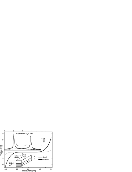
Since the resistance shows a peak in the the domain state of the F layers, we cannot interpret the data in terms of mechanisms which yield a decreased resistance (enhanced superconductivity) when the relative magnetization directions in the two F layers deviate from parallel. In principle, quasiparticle trapping could provide a mechanism for increased resistancerusanov06 . It would then have to be argued that the domain state locally leads to antiparallel configurations between the two F layers, as was actually found in the case of F/S/F trilayers involving (La,Ca)MnO3 and YBa2Cu3O7.pena05 However, in view of the weak pinning properties of the superconductor, another possibility is flux flow resistivity associated with the motion of vortices formed spontaneously above Bloch domain walls. The sample is in the force-free configuration () for the applied field, but induced vortices pointing out of the plane of the sample will feel a Lorenz force due to the applied current, which can cause vortex motion across the width of the wire. To clarify this, we measured current (I) - voltage (V) characteristics on the same sample GdNi(11)/MoGe(21)/GdNi(11) at 1.8 K, well below the transition, and with the field either at - or sligtly above +. They are shown in Fig.4, which also shows a sketch of the sample configuration, with the directions of applied field, current, and flux inside the F-layer (including the domain wall). At this temperature we find a true supercurrent, and a gradual onset of voltage. Using a 1V criterion, the critical currents in the low and high resistive states taken from Fig.4 are 640 and 340 A respectively. Resistance peaks at this temperature therefore can still be seen, as long as the bias current is large enough to depin the vortices. This is shown in the inset of Fig.4, where the voltage (resistance) was taken at a bias current of 1 mA.
The effect is not strongly sensitive to variation of the S and/or F layer thicknesses. This is demonstrated by the data in Fig. 5 in which MoGe layer is thicker, as well as the inset of Fig. 5 (thicker GdNi). These all show qualitatively similar switching behavior to the original sample. In the case of the thicker MoGe layer some additional features are observed around zero field. These are the two F layers switching independently, (also confirmed by magnetoresistance measurements above Tc - not shown here). This is most likely a combination of a reduction of the direct coupling between the F layers for thicker MoGe, and an increase of the roughness and therefore of the top GdNi layer for a thicker spacer. With thicker GdNi the is reduced, the peaks can shifted to below 0.1 mT leading to a sensitivity in the switching at the steepest part of the curve (increasing field sweep) /mT at an applied field of T. In Fig. 5 we also show the effect of patterning wires of different widths. The switching field changes from a 100m to 2m width due to shape anisotropy, and with it therefore the field at which vortices are present in the MoGe. This allows us further control over in complement to varying the thickness of the GdNi.

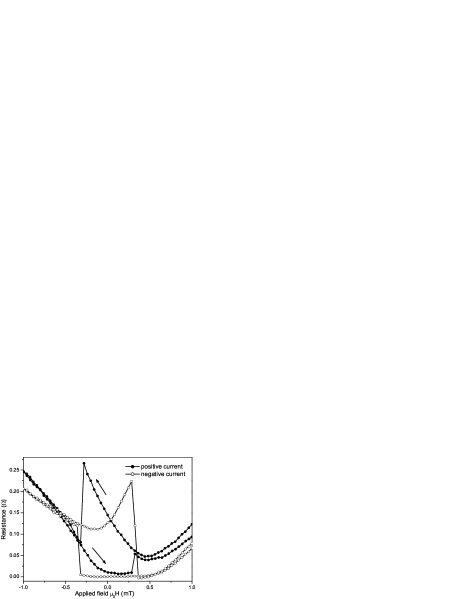
A point of interest is that in bilayer samples the switching behavior is less pronounced and also more complicated, since we now find asymmetry in the peak value of the voltage (resistance), but also asymmetry with respect to the current direction. Fields sweeps are shown in Fig. 6 for a bilayer sample MoGe(21)/GdNi(22), at a temperature of 3.88 K, near the bottom of the transition. For positive current (parallel to positive ) a jump rather than a peak is seen at , and a rather broad peak occurs at . We also observe an increasingly resistive background (suppression of the superconductivity) at higher fields. For the other current direction the reverse is the case: a peak in occurs at when sweeping from negative . Unraveling this behavior would need extensive study of the I-V characteristics, which will be for future work. We can, however, identify several differences between trilayers and bilayers. For instance, the bilayer is in fact asymmetric : the order parameter is strongly suppressed at the S/F interface, but not at the free interface, and vortex pinning may actually be sensitive to (inhomogeneities at) the free interface. Also, given the observation of only one resistance peak in the trilayer case it appears that the domain walls couple across the MoGe layer, at least for relatively thin MoGe. We made similar observations of only one resistance peak for trilayers with two different thicknesses of the F-layer, such as GdNi(11)/MoGe(21)/GdNi(22). We can speculate that this domain wall coupling both enhances the local flux density in the superconductor and sharpens the switching behavior.
IV Vortex formation
We have argued above that the magnetoresistive peaks we observe are due to vortices formed in the S layer above Bloch walls present in the F layer. To make this more compelling, we now estimate whether such vortices can actually be expected to form. For this we use the results from the model discussed recently by Burmistrov and Chtchelkatchev.burmistrov05 Basically, they find the amount of flux coming out of a Bloch wall of width situated in a ferromagnetic film of thickness characterized by a volume (saturation) magnetization , and from a free energy consideration calculate whether this can lead to the formation of a vortex in a superconducting layer of thickness , characterized by a London penetration depth , placed on top of the ferromagnet. For the case of a single domain wall they find, for given , , and , the minimum or critical magnetization needed to overcome the lower critical field of the superconductor. Since in our experiments is a materials constant, it is more convenient to write this condition in terms of a minimum thickness for the F-layer , which takes the form
| (1) |
Here, = if , otherwise
equals ; is given by , with the Ginzburg-Landau coherence length and
the flux quantum; G 0.916 is the Catalan constant, and units. For
MoGe, the relevant values are 0.7 m, which for a 20 nm film
yields 24.5 m; and 5 nm, leading to
1.8 A/m, an extremely low value which is due to the combination of a large bulk
penetration depth and a small film thickness. For GdNi, the relevant characteristic
are and . As discussed above, = 7.8 A/m
(corresponding to 0.98 T) is relatively large. Values for are not exactly
known, but the weak magnetocrystalline anisotropy leads to large wall widths, which
we take of order 1 m. The relevant limit is then ,
and eq. 1 yields = 2.9 nm. For the thicknesses we use, and
under the assumption of Bloch walls, the flux from a domain wall is therefore easily
large enough to create vortices.
This is the main conclusion from the calculation, but several more remarks are in
order. First, it is interesting to note that, in this limit, does not
depend on (apart from the logarithmic factor ), since . Then, we have disregarded the effect of the in-plane applied
field. In terms of the model, this is allowed since , which means
that the field fully penetrates without more than the vacuum contribution to the
free energy. Experimentally, it can be noted that misalignment effects are
apparently not relevant, since vortices are only created in significant amounts in
the domain state of the ferromagnet. Making a rough estimate, an applied field of
2 mT (outside the flux flow peak) under a 1∘ misalignment yields an
induction of A/m, again much smaller than the estimated .
Furthermore, we note that, although the flux density from the domain wall is well
above the lower critical field , it is still much lower than the upper
critical field . With a typical value of -
2.5 T/K, and taking T-Tc 100 mK, is found to be
0.25 T, very much larger than . In summary therefore, the
reason that vortices can be observed close to the resistive transition in our
MoGe/GdNi system is that the amorphous ferromagnet combines a reasonably large
magnetization with a large domain wall width, while the amorphous superconductor
combines a large penetration depth with a high upper critical field.
Given these different constraints, it is of interest to consider the possibility of vortex formation in various S/F systems which are currently under investigation as -junctions or spin switches, especially those based on Nb such as Nb/Py, Nb/Co or Nb/CuNi. The F layers in these combinations are qualitatively different, with Py having large and large , Co having large and small , and CuNi having small and larger . Also considered can be YBa2Cu3O7 (YBCO) and La0.7Ca0.3MnO3 (LCMO). For Nb, we use typical values of = 50 nm, = 50 nm, = 12 nm, for YBCO we use = 50 nm, = 180 nm, = 2 nm. The different values for the ferromagnets are given in Table 1, together with the computed value for . This is of course based on the assumption of Bloch and not Néel walls in such thin films, which may not be the case, but the numbers are instructive nonetheless.
| System | [T] | [m] | [nm] | () |
|---|---|---|---|---|
| a-MoGe/a-GdNi | 0.98 | 1 | 2.9 | 0.03 |
| Nb/Py | 0.7 | 1 | 5.7 | 16 |
| Nb/Co | 1.6 | 0.05 | 5.9 | 0.8 |
| Nb/CuNi(50) | 0.1 | 0.25 | 19.1 | 0.16 |
| Nb/CuNi(10) | 0.1 | 0.5 | 20 | 1.6 |
| YBCO/LCMO | 0.75 | 0.05 | 51 | 0.06 |
The table shows that the combination MoGe/GdNi actually yields the lowest value for due to the combination strong magnet / large domain wall. Still, for the strong magnetsthe numbers do not vary overmuch, is typically a few nm. For weak CuNi it is significantly larger, which is interesting in view of the observations of Ryazanov et al. ryazanov03 . They found flux flow behavior in the curves of a Nb wire at in-plane applied fields around the coercive field of a block of 18 nm thick CuNi on top of a portion of the wire and ascribed the effect to vortices induced in the S layer due to Bloch domain walls in the CuNi. Taking into account that the Nb layer in their case was only 10 nm thick, the estimated value is 20 nm, which is roughly the thickness used in the experiment. The Bloch wall scenario for this experiment appears not unreasonable, since the prepared state is in-plane magnetized, while CuNi has a tendency to perpendicular magnetization in this thickness range, as found for CuNi/Cu multilayers ruotolo04 . The largest value for is found for YBCO/LCMO, which is due to the large value of in this system.
V Conclusions
We have demonstrated that amorphous F/S/F heterostructures can show large magnetoresistance associated with vortex motion in the S layer, induced by magnetic domains in the F layers. This magnetoresistance can be several tens of Ohms change in a field step of a few tens of T due to the combination of weak domain wall and vortex pinning in these amorphous materials. We note that this effect can be a relatively simple test for the presence of Bloch domain walls in a ferromagnetic film. Also, the strong signals may provide a possibility to combine magnetic domain and flux logicallwood02 ; reichhardt04 in a flexible way, since we have demonstrated that both the GdNi thickness and wire widths can be effective tools to tune the fields at which the peaks in flux flow resistivity are observed. That said, we also should mention some problems open for further research. One point we have not touched is the obvious question whether the measured increase in resistance can be tied to flux-flow resistivity in a quantitative way from the standard formula , with the normal-state resistance. At the moment we cannot answer that question since, apart from the fact that our measurements have not been performed in the linear regime of the characteristics where homogeneous flow can be assumed, we know neither the local field, nor the amount of vortices (determined by the domain wall width) between the voltage contacts. Also disregarded in the discussion are possible geometrical effects which would lower the entry field for vortices due to an inhomogeneous current distribution. This touches different questions such as whether this allows smaller values than , but also whether the nucleation of magnetic domains, through their creation of vortices, actually is facilitated by edges or corners. Fabrication of structures with artificial nucleation points would be an interesting extension of the present work.
Acknowledgements.
We thank B. Leerink for preliminary measurements on the GdNi system, and R. Hendrikx and M. Hesselberth for X-ray and Rutherford Backscattering measurements. This work is part of the research programme of the ‘Stichting voor Fundamenteel Onderzoek der Materie (FOM)’, which is financially supported by the ‘Nederlandse Organisatie voor Wetenschappelijk Onderzoek (NWO)’.References
- (1) A. I. Buzdin, Rev. Mod. Phys. 77, 935 (2005).
- (2) L. R. Tagirov, Phys. Rev. Lett.83, 2058 (1999).
- (3) I. Baladié and A. Buzdin, Phys. Rev. B 67, 014523 (2003).
- (4) Y.Fominov, A. A. Golubov and M. Yu. Kupriyanov, Pis’ma Zh. Éksp. Teor. Fiz. 77, 609 (2003); [JETP Lett. 77, 510 (2003)].
- (5) J. Y.Gu, C.-Y. You, J. S. Jiang, J. Pearson, Y. B.Bazaliy and S. D. Bader, Phys. Rev. Lett.89, 267001 (2002).
- (6) A. Y.Rusanov, S. Habraken and J. Aarts, Phys. Rev. B 73, 060505(R) (2006).
- (7) R. J. Kinsey, G. Burnell and M. G. Blamire, IEEE Trans. Appl. Supercond. 11, 904 (2001).
- (8) Z. Yang, M. Lange, A. Volodin, R. Szymczak, and V. V. Moshchalkov, Nature Materials 3, 793 (2004).
- (9) M. Lange, M. J. Van Bael, and V. V.Moshchalkov, Phys. Rev. B 68, 174522 (2003).
- (10) W. Gillijns, A. Yu. Aladyshkin, M. Lange, M. J. Van Bael and V. V. Moshchalkov, Phys. Rev. Lett. 95, 227003 (2005).
- (11) V. V. Ryazanov, V. A. Oboznov, A. S. Prokof’ev and S. V. Dubonos, Pis’ma Zh. Éksp. Teor. Fiz. 77, 43 (2003); [JETP Lett. 77 39 (2003)].
- (12) I. S. Burmistrov, and N. M. Chtchelkatchev, Phys. Rev. B 72, 144520 (2005).
- (13) B. L. T. Plourde, D. J. Van Harlingen, N. Saha, R. Besseling, M. B. S. Hesselberth and P. H. Kes, Phys. Rev. B 66, 054529 (2002).
- (14) G. J. C. van Baarle, A. M. Troianovski, T. Nishizaki, P. H. Kes and J. Aarts, Appl. Phys. Lett.82, 1081 (2003).
- (15) K. Moorjani and J. M. D. Coey, Magnetic glasses (Elsevier, Amsterdam, 1984).
- (16) R. Asomoza, A. Fert, I. A. Campbell, A. Liénard and J. P. Rebouillat, J. Phys. F: Met. Phys. 9, 349 (1979).
- (17) We use a density of 6.0 at/m3, see A. Gangulee and R. C. Taylor, J. Appl. Phys. 49, 1762 (1978).
- (18) The magnetization even becomes slightly negative because of the diamagnetic contribution of the Si substrate.
- (19) V. Peña, Z. Sefrioui, D. Arias, C. Leon, J. Santamaria, J. L. Martinez, S. G. E. teVelthuis and A. Hoffmann, Phys. Rev. Lett. 94, 057002 (2005).
- (20) A. Ruotolo, C. Bell, C. W. Leung, and M. G. Blamire, J. Appl. Phys. 96, 512 (2004).
- (21) D. A. Allwood, G. Xiong, M. D. Cooke, C. C. Faulkner, D. Atkinson, N. Vernier and R. P. Cowburn, Science296, 2003 (2002).
- (22) C. J. Olsen Reichhardt, C. Reichhardt, M. J. Hastings and B. Jankó, Physica C 404, 266 (2004).