Large-scale electronic structure theory for simulating nanostructure process
Abstract
Fundamental theories and practical methods for large-scale electronic structure calculations are given, in which the computational cost is proportional to the system size. Accuracy controlling methods for microscopic freedoms are focused on two practical solver methods, Krylov-subspace method and generalized-Wannier-state method. A general theory called the ‘multi-solver’ scheme is also formulated, as a hybrid between different solver methods. Practical examples are carried out in several insulating and metallic systems with - atoms. All the theories provide general guiding principles of constructing an optimal calculation for simulating nanostructure processes, since a nanostructured system consists of several competitive regions, such as bulk and surface regions, and the simulation is designed to reproduce the competition with an optimal computational cost.
1 Introduction
Electronic structure theory plays a crucial role in understanding and controlling nanostructures, structures in nano-meter and ten-nano-meter scales. Dynamical simulation in these scales is, however, impractical for the present standard methodology, such as the Car-Parrinello method [1], owing to its heavy computational cost. From 1990’s, many calculation methods and related techniques have been proposed for large systems, systems with thousands of atoms or more, by calculating one-body density matrix or the Green’s function, instead of one-electron eigenstates. [2, 3, 4, 5, 6, 7, 8, 9, 10, 11, 12, 13, 14, 15, 16, 17, 18, 19] In these methodologies, calculation is carried out with real-space representation and a physical quantity is given as a trace form
| (1) |
Here the one-body density matrix is defined, from occupied one-electron eigenstates , as
| (2) |
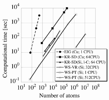
One can find that, if the matrix is of short range, the off-diagonal long-range component of the density matrix does not contribute to the physical quantity , which is important for practical success of large-scale calculations. [2] Actual calculation methods and their applications are found in recent reviews [3, 4] or papers. [5, 6, 7, 8, 9, 10, 11, 12, 13, 14, 15, 16, 17, 18, 19] A set of theories and program codes have been developed in our group and a test calculation of Fig. 1 shows that the computational cost is ‘order-’ or proportional to the system size () among the calculations with - atoms [15, 17, 16, 20, 19].
A practical success in an application study always requires the balance between the accuracy and the computational cost. Every calculation method has several controlling parameters and one should establish a systematic way of setting them in optimal values. Here we remember that a nanostructure is composed of several comparable regions with essential difference in electronic structure, such as bulk and surface regions. Since the competition of these regions gives various structural and functional properties of nanostructures, the requirement on dynamical simulation of a nanostructure is to reproduce the competition, or to reproduce the difference in electronic structure among the regions, throughout the process.
In this paper, we will show how to construct an optimal calculation scheme for nanostructure process. The essential concepts are (i) controlling method of the accuracy and the computational cost by monitoring residuals for microscopic or basis freedoms and (ii) choice or combination of different calculation methods. Hereafter the word ‘solver method’ is used as a practical calculation method of density matrix with a given Hamiltonian .
This paper is organized as follows; In Sec. 2, we will explain the foundation of two methods, Krylov subspace method and generalized Wannier state method. They are practical solver methods to calculate the density matrix for a given system and we will compare them, in Sec. 2.3, from a practical view point. In Sec. 3, we will construct a methodology of ‘multi-solver’ scheme, as a hybrid or combination of different solver methods. Several applications as molecular dynamics (MD) simulations will be presented in Sec. 4, so as to clarify the methodological points. In the present paper, we limit the formulations into those for a Hamiltonian as a real-symmetric matrix. Practical calculations were carried out with Hamiltonians in the Slater-Koster (tight-binding) form; The Hamiltonian for fcc Cu is constructed from the first-order form of the linear muffin-tin orbital theory [21] and those for C and Si are typical ones in Ref. [22] and Ref. [23], respectively.
2 Theory (1) Practical solver methods
2.1 Solver methods with Krylov subspace
Krylov subspace is a general mathematical concept defined as the linear space of
| (3) |
Here the ‘starting’ vector () and the dimension of the subspace () are arbitrary. Many iterative methods, such as the standard conjugate-gradient method, are formulated with Krylov subspace. See a recent textbook [24], for example. In the present context, the matrix is a Hamiltonian and is a real space basis. A large-scale calculation can be realized, when the density matrix is constructed within the Krylov subspace . The Krylov subspace method enables us also to calculate the Green’s function , which gives directly the information of electronic states, such as the density of states (DOS). When the dimension is equal to that of the original Hamiltonian matrix , the linear space of Eq. (3) is complete and all the calculation results are exact. [24]
2.1.1 Subspace-diagonalization method
Here we explain a practical solver method with Krylov subspace, called ‘subspace-diagonalization method’ (KR-SD) [16]; First, we construct an orthogonal basis set for the Krylov subspace ();
| (4) |
by the Lanczos procedure, a three-term recurrence formula. The -th basis is constructed in the -dimensional Krylov subspace (). In result, a reduced Hamiltonian matrix
| (5) |
is obtained as an explicit matrix. A typical subspace dimension is in MD simulations. Then, we diagonalize the reduced (small) matrix
| (6) |
with a negligible computational cost. The resultant eigen vectors are described as the set of coefficients .
The density matrix is obtained by
| (7) | |||||
| (8) |
with the definition of
| (9) |
Here the occupation number is given by the Fermi-Dirac function with a temperature (level-broadening) parameter and the chemical potential . The chemical potential is determined by the bisection method. The Green’s function can be calculated in a similar manner. [16] In short, the present procedure is a standard quantum-mechanical calculation for eigen states, except the point that the calculation is carried out within the Krylov subspace. Therefore it is straightforward to apply the method to calculations with a nonorthogonal basis set, in which a generalized eigen-value equation, instead of Eq. (6), is solved within the subspace.
2.1.2 Shifted conjugate-orthogonal conjugate-gradient method
Another solver method with Krylov subspace was formulated and called ‘shifted conjugate-orthogonal conjugate-gradient’ (SCOCG) method. [19] Its foundation is given by a mathematical theorem proved recently. [25] The practical procedure is based on an iterative solver method for the linear equation of the Green’s function;
| (10) |
because of . The density matrix is obtained by
| (11) |
The SCOCG method and KR-SD method share many common features but are different in the numerical treatment. See the original paper [19] for detailed comparison. For the present time, we use, mainly, the KR-SD method for MD simulation and we think that the SCOCG method is suitable to discuss a very fine energy spectrum of the Green’s function. [19]
2.1.3 Accuracy control with residual
So as to monitor the accuracy during the simulation, we calculate a residual vector of the Green’s function; [19]
| (12) |
The residual vector is defined individually among the basis suffix . We observed that the required subspace dimension for a given criteria on the residual vector is different among surface and bulk regions. [19] Such a determination of the controlling parameters is an example of the accuracy control for microscopic or basis freedoms.
2.2 Solver methods with generalized Wannier state
Another method for obtaining the density matrix in large systems is formulated using generalized Wannier state. [26, 27, 5, 7, 28, 11, 29, 30] A physical picture of the generalized Wannier states is localized chemical wave function in condensed matters, such as a bonding orbital or a lone-pair orbital with a slight spatial extension or ‘tail’. [5, 7, 28, 11, 29, 30] Their wavefunctions are equivalent to the unitary transformation of occupied eigen states and satisfy the equation of
| (13) |
where the matrix is the Lagrange multipliers for the orthogonality constraint . The suffix of a wavefunction indicates the position of its localization center, such as bond site. Since Wannier states give the density matrix in Eq. (2) by replacing eigen states into Wannier states , any physical quantity can be reproduced in the trace form of Eq. (1).
Our practical solver methods are based on a mapped eigen-value equation [11, 31] that is equivalent to Eq. (13);
| (14) |
where
| (15) | |||
| (16) |
The energy parameter should be much larger than the highest occupied level. Equation (14) was derived in Refs. [11, 31] and will be derived again, from a different theoretical background, in Sec. 3.1 of this paper.
2.2.1 Variational procedure in Wannier-state method
Equation (14) gives a practical iterative procedure to generate Wannier states under explicit localized constraint, [11, 15, 17, 31] which is called variational Wannier state method. See papers [11, 31] for details. Residual vector for each wavefunction
| (17) |
is monitored for each Wannier state during the simulation, so as to control the accuracy, which realizes the accuracy control for microscopic or basis freedoms, as discussed in the Krylov-subspace method with Eq. (12). A practical success in the Wannier-state method is realized, when all or a dominant number of wavefunctions are well localized. Examples and technical details are given in Sec. 4.2 and references [11, 15, 31].
2.2.2 Perturbative procedure in Wannier-state method
We developed also a perturbative method, [11, 29, 32, 31] in which a perturbation solution of Eq. (14) is constructed for each Wannier state ;
| (18) |
Here and are the unperturbed and first-order perturbation terms, respectively, and the factor is the normalization factor. The unperturbed term should be prepared as an input quantity and the perturbation term and the normalization factor are determined automatically by the standard first-order perturbation procedure. [11, 29, 32, 31] During a simulation, the weight of the unperturbed term
| (19) |
is monitored, for each wavefunction, as an accuracy control for microscopic or basis freedoms. In silicon crystal, for example, the ideally -bonding wavefunction is chosen as the unperturbed term and the weight of the unperturbed term is dominant () [11, 29, 31], which validates the perturbative treatment. When the perturbative method is validated, its computational performance is faster than that of the variational method, since the perturbative method gives a simpler procedure to generate the wavefunctions and does not require any iteration loop.
2.3 Comparison between Krylov-subspace and Wannier-state methods
When the Wannier-state methods are compared with the Krylov-subspace methods, the Wannier-state methods require an initial guess of wavefunctions in the variational (iterative) method or an unperturbed term of wavefunction in the perturbative method. As an example, the reconstruction on Si(001) surface was calculated with the force on atoms. The calculation was carried out by the two Krylov-subspace methods, (i) the subspace diagonalization procedure [16] and (ii) the SCOCG procedure [19], and (iii) the variational Wannier-state method. [31] In the variational Wannier-state method, the initial guess of the wavefunctions are prepared to be the lone-pair state of for surface states and to be the -bonding states for other (bulk) states. The three methods reproduce the energy differences satisfactorily among the , , and surfaces, when these results are compared with those of the eigen-state calculation with the present Hamiltonian [33] and the standard ab initio calculation [34].
The perturbative Wannier-state method is much limited in its applicability than the above three methods, because the unperturbed term should be prepared as a good approximation ( or ). So far we have applied the perturbative Wannier-state method only to the bulk (-bonding) wavefunction in the diamond-structure solids without deformation or with small (elastic) deformation. [11, 29, 32, 31] Since the first-order perturbation form was used for the wavefunction in these cases, the calculated energy is correct within the second order with respect to deformation and the elastic constants are well reproduced. We should say, however, that a drastic change of wavefunction, like that in a bond-breaking process, is not reproduced by the perturbative Wannier-state method, if the bulk (-bonding) wavefunction is chosen as the unperturbed term.
Despite the limitations, the computational performance of the Wannier-state methods is faster, at best by several hundred times, than that of the Krylov-subspace method, if it is applicable. In Fig. 1, for example, the Wannier-state method with the perturbative procedure (WS-PT) using single CPU is faster than the Krylov-subspace method with the subspace-diagonalization procedure (KR-SD) using 64 CPUs.
When one thinks about a guiding principle for how to choose a solver method in an application study, the above discussion suggests that the Wannier-state methods give a faster performance, when the input wavefunctions are near the final solutions and, particularly, they are well localized. In other cases, the Krylov-subspace method is preferable, since the Krylov-subspace method does not require any input quantity for electronic states.
3 Theory (2) Multi-solver scheme
3.1 Formulation
As another fundamental methodology for large-scale calculations, we developed a ‘multi-solver’ scheme [15, 31], as hybrid or combination of two different solver methods. Its basis idea is that the density matrix is decomposed into two parts called ‘subsystems’ and they are given by different solver methods. As discussed below, the multi-solver scheme will be fruitful, particularly, when the simulation system is composed of different regions, such as bulk and surface regions, and different solver methods are used in these different regions.
The mathematical foundation of the multi-solver scheme is based on the commutation relation of the density matrix;
| (20) |
When the occupied one-electron states, eigenstates or Wannier states, are classified into two groups A and B, the density matrix is decomposed into the corresponding two parts
| (21) |
where
| (22) | |||
| (23) |
Here we call and ‘subsystems’ and the two subsystems are orthogonal
| (24) |
owing to the orthogonality relation
| (25) |
If the subsystems are defined from eigenstates, a mapped Hamiltonian
| (26) |
with a scalar , satisfies the commutation relation
| (27) |
owing to Eq. (24) and
| (28) |
We call the scalar ‘energy-shift parameter’. If is given, the problem for obtaining is reduced to a standard quantum mechanical problem with the well-defined Hamiltonian . In practical calculations, the energy shift parameter is chosen to be so large that the states in do not lie in the occupied energy region of . Note that Eqs. (27), (28) are satisfied, even if the subsystems are constructed by eigen states with fractional occupancy.
If the subsystems are defined from Wannier states, on the other hand, Eq. (27) are not satisfied, because Eq. (28) is not satisfied. Then we redefine the mapped Hamiltonian as
| (29) |
which satisfies Eq. (27) in the cases of eigenstates and Wannier states. See A for proof. A simplest case is that the subsystem is consist of only one Wannier state . In this case, the mapped Hamiltonian in Eq. (29) is reduced to that in of Eq. (15), because of and . In other words, the present theory gives another derivation of Eq. (14), the mapped equation of Wannier state. From a practical view point, the term in Eq. (29) can be ignored, when the energy shift parameter is so large that the energy band of is well separated, energetically, from that of . If the term is ignored, the mapped Hamiltonian is reduced to the form of Eq. (26).
3.2 Example 1
Hereafter, the multi-solver scheme will be demonstrated. Although the formulation of the multi-solver scheme is general, we have used, so far, the scheme only with the perturbative Wannier-state method for a subsystem (). Among these cases, the subsystem is determined in the first-order perturbation form, and then the other subsystem is determined, through the mapped Hamiltonian , by a different solver method (). In other words, the present procedure does not contain a self-consistent loop (). A related general discussion will be given in Sec. 4.3.
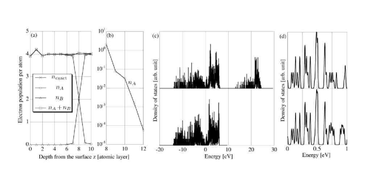
The first example is a Si slab with ideal (001) surface, in which we use the eigen-state method for and the perturbative Wannier-state method for . Each atomic layer contains 64 atoms and the total number of atoms is in the periodic simulation cell. Since an ideal (001) surface gives an almost zero energy gap (0.025 eV), the present example is one of the severest tests for the present methodology. The coordinate is written in the unit of atomic layer (). The surface atoms are located at and have dangling-bond electrons. The atoms in the opposite surface () are terminated by the bulk (sp3-bonded) Wannier states and do not have any dangling-bond electrons. The coordinate of bulk-bond sites can be described as half integers . In the multi-solver scheme, the subsystem is constructed from the Wannier states whose localization (bond) centers are located deeper than the eighth atomic layer (). The rest system is assigned to the subsystem that contains the surface states. The wavefunctions in are determined by the perturbation form and, then, is determined by diagonalizing the mapped Hamiltonian . The energy shift parameter is chosen as a.u. ( 27.2 eV).
In Fig. 2(a), the electron populations of the subsystems, and , are plotted as the function of the atomic coordinate . The total electron population in the multi-solver scheme reproduces the exact one . As a remarkable result, the population at is contributed by both of the subsystem and with an almost equal weight, since the Wannier states located at and those at belong to and , respectively. Figure 2(b) shows that decays quickly at , because of the nature of the mapped Hamiltonian .
So as to understand the multi-solver scheme, Figs. 2(c)(d) show the DOS of the original Hamiltonian and the mapped Hamiltonian . The energy origin () is chosen at the lowest unoccupied level in . Each eigen level is drawn as a spike with the width of eV. In the DOS of the mapped Hamiltonian, the band in the occupied energy region () is that of , while the band of is shifted by , owing to the term of in , and is located at the high-energy region at . As in Fig. 2(d), the two DOS profiles agree excellently at the bottom of the unoccupied energy region (eV). Here we recall that the original and mapped Hamiltonians, from their definitions, share the unoccupied eigen states that gives the density matrix of () and the disagreement in the present result appears only because is deviated from the exact one. The excellent agreement at the band bottom (eV) appears, since these states are contributed dominantly by surface states and are almost free from the subsystem .
3.3 Example 2
The multi-solver scheme was demonstrated in large-scale calculations. The first example is reconstructed (001) surface of Si slab with atoms, which is determined with the force on atoms. The practical procedure is the same as in Sec.3.2, except the point that the subsystem is calculated by the Krylov-subspace (KR-SD) method instead of the exact diagonalization method. The result shows the correct surface reconstruction. [16]
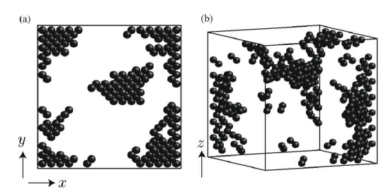
The second example is a MD simulation of a silicon nanocrystal with 4501 atoms. The the multi-solver scheme is constructed from the variational Wannier-state method for and the perturbative Wannier-state method . [31] An external load is imposed in the [001] direction and one initial defect bond is introduced by imposing a repulsive force on an atom pair. The sample is deformed with external load, the initial defect bond and thermal motion but not fractured. The subsystems, and , are assigned automatically during the MD simulation, as explained below; First, all the wavefunctions are calculated by the perturbative solver method, in which the weight of the unperturbed term is defined for each wavefunction . (See Sec. 2.2) If the weight of a specific wavefunction is less than 95 % of the averaged weight (), the corresponding wavefunction is assigned into the subsystem and is determined by the variational procedure. In other words, if the perturbative procedure does not give a satisfactory accuracy, the procedure is switched automatically into the variational one. The result of the automatic assignment is shown in Fig. 3, in which atoms are visible, only if its electron population is significantly contributed from . As a result, the subsystem , treated by the variational procedure, appear mainly near the sample edges and in the internal region near the initial defect bond, because these regions are significantly deformed and the electronic states in these regions are fairly deviated from that in ideal crystal.
As a technical detail of the MD simulation with the multi-solver scheme, we used a fine tuning technique of lattice constant; [31] In calculations of ideal silicon crystal, the equilibrium lattice constant or bond length differs by 2 % between the variational and perturbative methods. The difference can cause, in principle, an artificial lattice mismatch in the multi-solver scheme and therefore we tuned the bond length, by imposing an additional two-body classical potential on an atom pair or bond site, if the atom pair is occupied by a perturbative Wannier state. This fine tuning technique avoids the possible artificial lattice mismatch. Although the calculation results without the fine tuning (not shown) did not indicate any practical problem among our calculations of silicon, we presume that an error of 2 % in lattice constant might be non-negligible in several cases. For example, the lattice constant between Si and Ge is different by 4 % and the artificial lattice mismatch by 2 % might cause a problem, when a Si/Ge system is calculated.
4 Applications
4.1 Liquid carbon : a metallic system
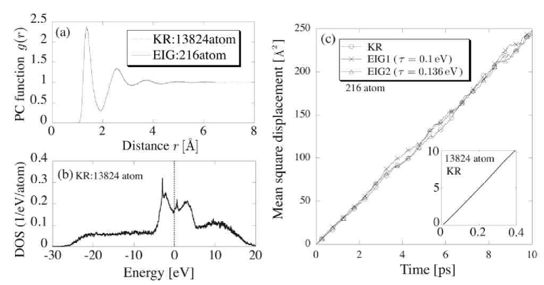
Liquid carbon was simulated with the Krylov-subspace method as a test calculation. The cubic simulation cell is used with 216 and 13824 atoms. The density and the temperature are set to be g/cm2 and K, respectively. The time interval between MD steps is set to be fs. As technical details, the subspace dimension and the number of atoms in the real-space projection (See B) are chosen to be and , respectively.
Figure 4(a) shows the resultant pair correlation (PC) function for the conventional eigen-state method with 216 atoms and for the Krylov-subspace method with 13824 atoms. The two graphs are indistinguishable, owing to an excellent agreement. In Fig. 4(b), the DOS is calculated, from the Green’s function, by the Krylov subspace method with 13824 atoms. In the DOS calculation, the controlling parameters are set into a heavier computational cost ( and ), so as to reproduce the fine DOS profile. Since the present Hamiltonian includes only and orbitals, the resultant DOS is missing in higher energy regions. The imaginary part of the energy is chosen at eV. The resultant DOS profile in Fig. 4(b) shows the correct feature of liquid carbon, as follows; A narrow band appears, from eV to eV, as in nanotubes, which can be decomposed the bonding and antibonding bands. The bond in liquid phase is, however, imperfect and non-bonding (atomic) states appear as a sharp peak near the chemical potential (eV).
Figure 4(c) shows the resultant mean square displacement (MSD) for the Krylov subspace method (KR) and the conventional eigen-state method (EIG1,EIG2). The main figure shows a system of 216 atoms by the two methods, while the inset shows that of 13824 atoms by the Krylov subspace method. In the eigen-state method, the level-broadening (temperature) parameter in the Fermi-Dirac function is set to eV (EIG1) and eV (EIG2), respectively, so as to show that the detailed treatment near the Fermi level causes different fluctuation behaviors of the MSD. Since the difference in fluctuation behavior is seen even among the two cases of the eigen-state method, we conclude that the Krylov subspace method shows satisfactory agreements with the eigen-state method for PC function and diffusion constant (the gradient of the linear behavior in the main figure of Fig. 4(c)).
4.2 Silicon : cleavage process
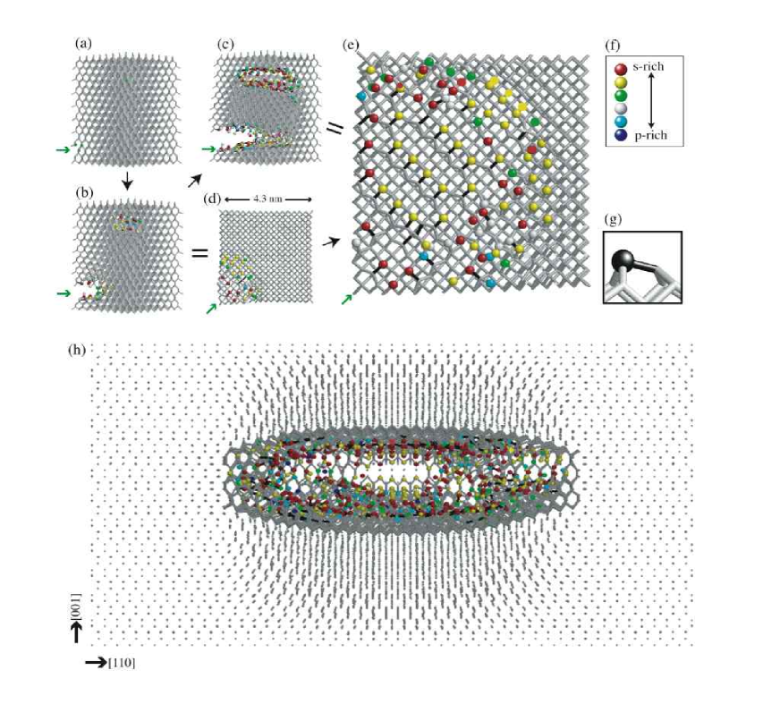
As a practical large-scale calculation, silicon cleavage process was investigated. [15, 31, 17] The Wannier-state method is used, since it is faster than the Krylov-subspace method, when, as discussed in Sec. 2.3, a dominant number of wavefunctions are well localized. The number of atoms in the localization region for each Wannier state () is assigned to be , which is determined by the residual norm . The resultant density matrix has a spatial spread, in its off-site elements, over regions with hundreds of atoms. Particularly, wavefunctions near cleaved regions tend to have a large residual norm and the localization constraint on such wavefunctions are automatically relaxed to increase the number . We found that such a way of controlling the accuracy for microscopic freedoms is crucial for reproducing the surface reconstruction on cleaved surface. See Ref. [31] for details.
Figure 5(a)-(c) shows a silicon cleavage process with the variational Wannier-state method. The external load is imposed on the direction, as in our previous simulation [15]. The present system, unlike the previous one [15], does not contain any initial defect for ‘cleavage seed’. In result, the cleavage starts from two points on the sample edges and two cleavage planes appear. The lower cleavage surface is shown in Figs. 5(d) and (e). In Fig. 5, a rod (atomic wavefunction) or ball (bonding wavefunction) is assigned for each wavefunction, according to the weight distribution among atoms. The black rods are the reconstructed bonds that are not seen in the initial (crystalline) structure. A ball is assigned for an atomic (non-bonding) orbital, localized on an atom site. On the cleaved surface, an asymmetric dimer appears, as on a clean (001) surface, with a ball (lone-pair state) on the upper atom, which is shown in Fig. 5(g). For quantitative discussion of orbital freedoms, a parameter is defined, [15] for a wave function , as
| (30) |
where is the s orbital at the -th atom. For example, in an ideal hybridized state. To visualize the orbital freedom of wave functions, the atomic (non-bonding) states are classified by the color of ball, according to the value of (See the caption of Fig. 5). After a bulk (sp3) bond is broken, the corresponding wavefunction is stabilized with increasing the weight of orbitals (), which results in appearance of red or yellow balls on cleaved surface.
As a remarkable result, a well-defined dimer-row domain is formed by nine dimers in Fig. 5(e), in which the tilting freedoms of asymmetric dimers are fixed into the configuration, although the surface energy of the surface is higher than that of the surface (See Sec. 2.3). We suggest that the directional anisotropy of deformation is caused by the cleavage propagation direction, as indicated by the green arrow in Fig. 5(e), and gives the ordering of the tilting freedoms into the configuration. We also calculated many other systems (not shown) in different sample geometry, which supports the above suggestion.
Figure 5(h) is a larger system simulated by the multi-solver scheme, in which we use the variational and perturbative Wannier-state methods for subsystems and , respectively. [15, 31] The system contains 118850 atoms and the sample dimension is in the unit of the atomic layers, where corresponds to about 20 nm. Here the subsystem was composed of selected Wannier states near fracture regions and the rest part of the electron system is defined as the subsystem . The number of Wannier states in the subsystem is approximately 5 % of the total and the computational cost by the present multi-solver scheme is nearly of that by the single-solver calculation with the variational procedure. In Fig. 5(h), the electronic states in the subsystem are depicted as rods or balls and those in the subsystem are invisible. The cleave surface in Fig. 5(h) contains (001) surface but is fairly unstable with many step formations. [15, 31] See Refs. [15, 17] for the physical discussion of the instability.
4.3 General discussion on the multi-solver scheme
Finally, a general discussion is made for a practical application of the multi-solver scheme. Among the present examples, the procedure was carried out without a self-consistent loop (), as explained in the beginning of Sec. 3.2. The present non-selfconsistent procedure is practical, particularly, if the electron system can be decomposed into two parts that are governed by stronger and weaker binding mechanisms, respectively. In the present examples, the electronic states in the bulk part () are governed by a stronger binding mechanism (the bonding) than those in surface states () and can be well described without any detailed information of the surface states (). Another example of the decomposition may be a system with strong bonds and weak bonds. The situation of the decomposition is a candidate of the multi-solver scheme. When the multi-solver scheme is used, the solver method for each subsystem should be chosen from the discussion of Sec. 2.3.
We note that the multi-solver scheme with a self-consistent loop can be realized, in principle, and its practical application might be a possible future work.
5 Concluding remarks
This paper presents fundamental theories and practical methods for large-scale electronic structure calculations, particularly for dynamical process with nm-scale or 10-nm-scale structures. First, we presented several practical solver procedures, based on Krylov subspace and generalized Wannier state, so as to obtain the density matrix without calculating eigen states. We emphasized that every method has a way of accuracy control for microscopic freedoms, by monitoring the residuals of exact equations. Second, the ‘multi-solver’ scheme was formulated based on the commutation relation of the density matrix and was used for a hybrid or combined method of different solver methods. Several practical large-scale calculations were carried out in metallic and insulating cases.
These methodologies enable us to design a simulation of nanostructure process with an optimal computational cost, in which the accuracy is controlled dynamically for microscopic (basis) freedoms and solver methods may be different among different regions. These points are essential in nanostructured systems, nm-scale or 10-nm-scale systems, because a competition between different regions, such as bulk and surface regions, is essential and is required to be reproduced in simulation. Since the above requirement is general among nanostructure processes, the present discussion is always valid, even when a different system is calculated by a different solver method from those in the present paper.
Appendix A Proof of the fundamental equation in the multi-solver scheme
Here we prove Eq. (27), the fundamental equation in the multi-solver scheme, when the subsystems , are constructed from Wannier states in Eqs. (22) and (23) and the mapped Hamiltonian is defined by Eq. (29). We notice that the projection operator onto the unoccupied Hilbert space, , is defined as
| (31) |
and satisfies
| (32) |
Equation (27) is satisfied as follows;
| (33) | |||||
where the second equality is obtained by Eqs. (24) and the fourth and sixth equality is obtained by Eq. (31) and Eq. (32), respectively. The last equality is obtained by the orthogonality relation of .
Appendix B Technical details and numerical aspects of the Krylov-subspace method
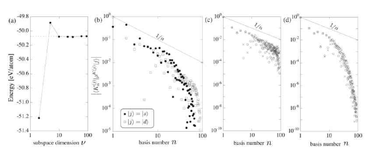
Here we discuss several technical details of the Krylov-subspace method and demonstrate how the method works, particularly in metals. As a demonstration, a fcc Cu system was calculated with a periodic simulation cell of atoms. The temperature (level-broadening) parameter in the Fermi-Dirac function is set to be eV. As a practical technique, a real-space projection technique is introduced; The Krylov subspace is generated by a Hamiltonian projected in real space, , instead of the original one , where the projection operator projects a function onto the spherical region whose center is located at the atomic position of the -th atomic basis. The resultant Krylov subspace is the same as the original one , while the bases lie within the projection region ( ). Since the procedure of constructing the Krylov subspace is independent among the starting bases , all the procedures and the quantities are well-defined with the real-space projection technique. The projection radius is determined for each starting basis , so that a given number of atoms, , should be contained inside the radius. The present calculation with atoms was carried out using the projection technique with . The calculation without the projection technique was also carried out in a smaller (876-atom) system, which is discussed below.
In Fig. 6(a), the convergence behavior of the calculated band structure energy is shown as the function of the subspace dimension, in which a reference value is also calculated by standard eigen-state calculation with the standard Brouillion-zone integration. The deviation from the reference value is about 0.01 eV per atom for 10, 20 and 30 and less than 1 meV per atom for and 90. Since the density matrix is calculated in the form of Eq. (8), its representation within the Krylov subspace is plotted in Fig. 6(b), where the starting bases are set to be and () orbitals, as examples. In Fig. 6(b), we observe a or faster decay, and this observation is also seen with the other staring bases ( and orbitals). The decay behavior of Fig. 6(b) is explained by a general mathematical analysis of the Lanczos procedure [16], in which a decay should appear with the zero-temperature formulation () and a faster decay should appear with a finite temperature formulation (). The quantity , on the other hand, also decays as or faster (not shown), since the (normalized) vector has a spatial spread within -th hopping range from the starting basis (). Consequently, their product () decays as or faster, which validates the fast convergence in the summation of Eq. (8).
We should emphasis that the decay behavior in Fig. 6(b) comes from a general property of the Lanczos procedure, as discussed above, not from the projection technique. The above statement is confirmed numerically in Figs. 6(c)(d), in which fcc Cu systems were calculated with or without the real-space projection and the resultant decay behavior is affected significantly by the temperature (level-broadening) parameter , but not by the projection technique.
References
- [1] Car R and Parrinello M 1985 Phys. Rev. Lett. 55 2471
- [2] Kohn W 1996 Phys. Rev. Lett. 76 3168
- [3] Galli G 2000 Phys. Status Solidi B217 231
- [4] Wu S Y and Jayamthi C S 2002 Phys. Rep. 358 1
- [5] Mauri F Galli G and Car R 1993 Phys. Rev. B47 9973
- [6] Li X-P Nunes R W and Vanderbilt D 1993 Phys. Rev. B47 10891
- [7] Ordejón P Drabold D A Grumbach M P and Martin R 1993 Phys. Rev. B48 14646
- [8] Goedecker S and Colombo L 1994 Phys. Rev. Lett 73 122
- [9] Hoshi T and Fujiwara T 1997 J. Phys. Soc. Jpn. 66 3710
- [10] Roche S and Mayou D 1997 Phys. Rev. Lett. 79 2518
- [11] Hoshi T and Fujiwara T 2000 J. Phys. Soc. Jpn. 69 3773
- [12] Ozaki T and Terakura K 2001 Phys. Rev. B64 195126
- [13] Soler J M Artacho E Gale J D García A Junquera J Ordejón P and Sánchez-Portal D 2002 J. Phys.:Condens. Matter 14 2745
- [14] Bowler D R Miyazaki T and Gillan M J 2002 J. Phys. Condens. Matter 14 2781
- [15] Hoshi T and Fujiwara T 2003 J. Phys. Soc. Jpn. 72 2429
- [16] Takayama R Hoshi T and Fujiwara T 2004 J. Phys. Soc. Jpn. 73 1519
- [17] Hoshi T Iguchi Y and Fujiwara T 2005 Phys. Rev. B72 075323
- [18] Skylaris C-K Haynes P D Mostofi A A and Payne MC 2005 J. Chem. Phys. 122 084119
- [19] Takayama R Hoshi T Sogabe T Zhang S-L and Fujiwara T 2006 Phys. Rev. B73 165108
- [20] Hoshi T Takayama R Iguchi Y and Fujiwara T 2006 Physica B 376-377 975
- [21] Andersen O K and Jepsen O 1984 Phys. Rev. Lett. 53 2571
- [22] Xu C H Wang C Z Chan C T and Ho K M 1992 J. Phys. Condens. Matter 4 6047
- [23] Kwon I Biswas R, Wang C Z, Ho K M and Soukoulis C M 1994 Phys. Rev. B 49 7242
- [24] van der Vorst H A 2003 Iterative Krylov methods for large linear systems (Cambridge: Cambridge University Press)
- [25] Frommer A 2003 Computing 70 87
- [26] Kohn W 1973 Phys. Rev. B7 4388
- [27] Kohn W 1993 Chem. Phys. Lett. 208 167
- [28] Marzari N and Vanderbilt D 1997 Phys. Rev. B56 12847
- [29] Hoshi T and Fujiwara T 2001 Surf. Sci. 493 659
- [30] Andersen O K Saha-Dasgupta T and Ezhov S 2003 Bull. Mater. Sci. 26 19
- [31] Hoshi T 2003 Docter Thesis (Tokyo: School of engineering, University of Tokyo)
- [32] Geshi M Hoshi T and Fujiwara T 2003 J. Phys. Soc. Jpn. 72 2880
- [33] Fu C C, Weissman M and Saúl A 2001 Surf. Sci. 494 119
- [34] Ramstad R Brocks G and Kelly P J 1995 Phys. Rev. B 51 14504