Quantum point contact due to Fermi-level pinning and doping profiles in semiconductor nanocolumns
Abstract
We show that nanoscale doping profiles inside a nanocolumn in combination with Fermi-level pinning at the surface give rise to the formation of a saddle-point in the potential profile. Consequently, the lateral confinement inside the channel varies along the transport direction, yielding an embedded quantum point contact. An analytical estimation of the quantization energies will be given.
1 Introduction
Structures based on quasi-1D nanocolumns are not only of major interest for basic research in the area of quantum transport but can also be considered as prototype systems of future nanodevices for information technology. Research in this field has attracted much attention recently due to the fact that nanocolumns can be fabricated either by employing self-organized growth modes or by lithographic patterning using a top-down approach Ref_NL5_2470 ; Ref_APL81_4458 ; Ref_PhysE25_2004 ; Ref_NL3_149 ; Ref_NL5_981 . In any case, due to their lateral dimensions in the nanometer regime, quantum confinement effects are expected to arise in such nanocolumns, leaving their signatures in the electronic transport properties. As a common feature, most of the application-relevant semiconductor material systems exhibit Fermi-level pinning at the outer surface due to surface states. Depending on the energetic position of the neutrality point, either surface depletion or surface accumulation occurs. In the following, we will consider the class of surface-depleted semiconductors such as GaAs or GaN. For nanocolumn systems, the spatial extent of the system can approach the size of the depletion region and lateral quantum confinement effects gain considerable influence on the electronic spectrum. The depletion length strongly depends on space charge, for example due to ionized doping impurities. Hence, doping profiles in combination with surface pinning have a significant influence on the potential profile on a nanometer length scale inside the nanocolumn channel.
We will discuss how nanoscale doping profiles inside a nanocolumn in combination with Fermi-level pinning at the surface give rise to the formation of a saddle-point in the potential. As a result, the lateral confinement inside the channel varies along the transport direction, yielding an embedded quantum point contact without the need for any heterostructure. In the following sections, we give an analytical estimation of the quantization energies and discuss a realistic example.
2 Nanocolumn confinement potential
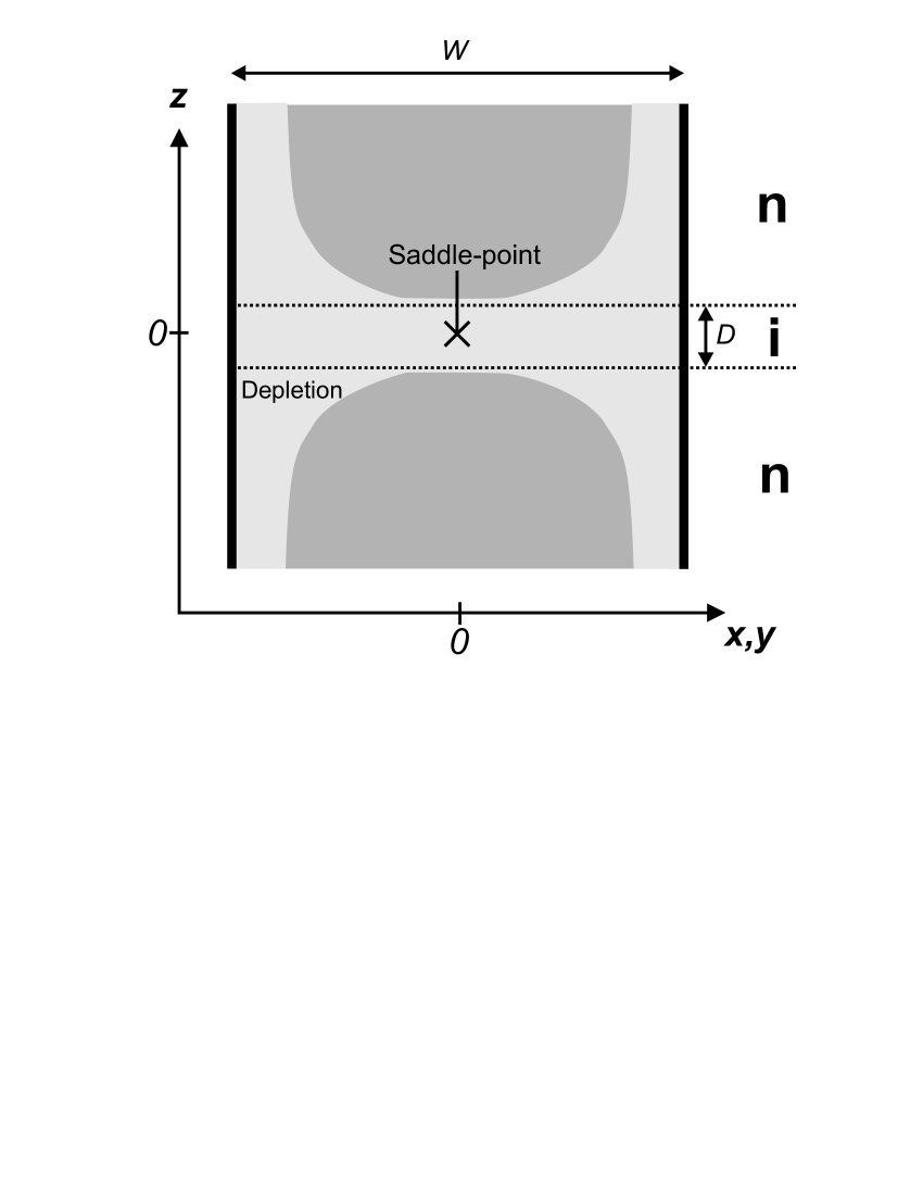
In order to visualize the interplay between surface pinning and doping profiles, we now consider a typical example of a cylindrical nanocolumn with an embedded doping profile as depicted in Fig. 1. Here, the main feature consists of a nanoscale intrinsic () layer between two -doped contact regions, perpendicular to the transport direction.
The Poisson equation for the conduction band profile (electronic potential energy) reads as
| (1) |
for a given charge density , and . As a boundary condition, we assume Fermi-level-pinning at the outer surface of the nanocolumn. Furthermore, the system is assumed to be rotational invariant within the -plane. Note that and have to be determined self-consistently, containing contributions from free electrons and ionized donors. In general, such a nanoscale problem requires a quantum statistical approach and cannot be solved analytically. In the following, we thus provide a simplified analytical estimation for the expected behavior.
For a homogeneously doped nanocolumn, the potential profile can be constructed to a good approximation by the well-known harmonic Schottky depletion model as depicted in Fig. 2(a). For a given donor concentration one obtains a depletion length of
| (2) |
This expression for represents a good approximation for the cylindrical column if . (For a more general discussion of the Poisson problem in systems with cylindrical symmetry see Refs. Ref_SSE46_885 ; Ref_JE_63_1115 ].)
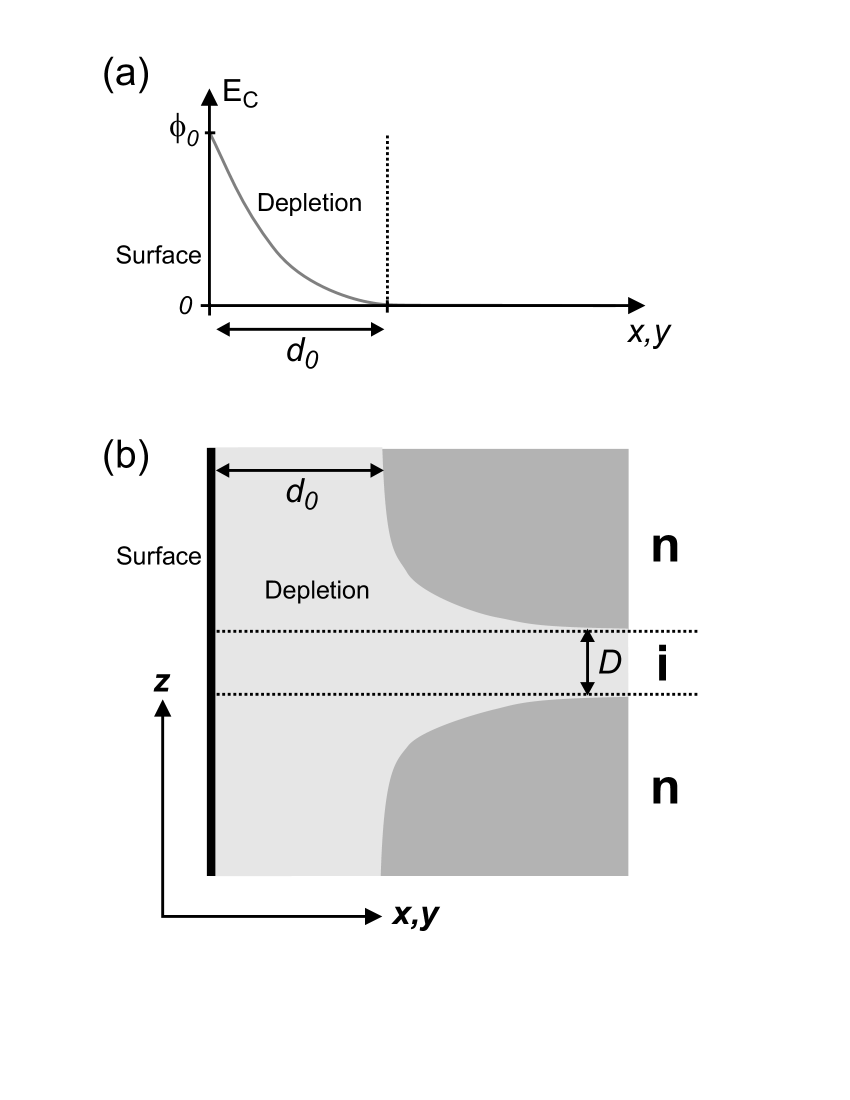
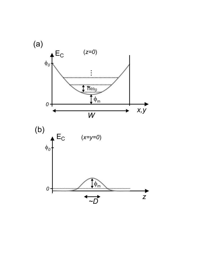
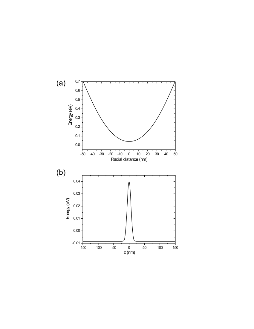
For the structure, we insert an intrinsic layer of thickness as sketched in Fig. 2(b). Due to within the intrinsic layer, the resulting must exhibit compensating curvatures in and . The overall potential within the intrinsic layer thus must exhibit a saddle-point as visualized in Fig. 1, exhibiting a minimum (confinement in the constriction) in -direction and a maximum (barrier) in -direction. The cross-sectional potential within the -plane at is plotted qualitatively in Fig. 3(a), whereas the potential along the center axis () is sketched in Fig. 3(b). The resulting lateral quantization energy varies with along the center axis, exhibiting the maximum value at which thus provides a quantum point contact (constriction) within the channel of the nanocolumn. This qualitative finding is a consequence of surface pinning in combination with the doping profile on a nanometer scale. It is a unique feature of the considered nanocolumn system, not found in bulk device structures and does not require any built-in heterostructure.
Four relevant length scales exist for this system (see also Fig. 1): The column diameter , the intrinsic layer thickness , the homogenous Schottky depletion length as defined in Eq. (2), and the “pinning de Broglie wavelength”
| (3) |
for an effective electron mass and the given . For realistic system parameters , an approximate expression for the potential profile in the vicinity of the saddle-point can be given: Within the -plane at , we can write (see also Fig. 3(a))
| (4) |
with the effective mass and the the harmonic oscillator frequency . From the pinning boundary conditions at we readily obtain
| (5) |
Furthermore, along the -axis at , we can approximate (see also Fig. 3(b))
| (6) |
with a positive constant . The width of this barrier is determined by a length scale and this yields
| (7) |
(The proportionality factor between and is of the order of 1. In general, it may depend on and and can be determined numerically, see Sec. 3.) From the condition we finally obtain for the barrier height
| (8) |
and the quantization energy within the saddle-point
| (9) |
This result can be recast as
| (10) |
3 Realistic example
In order to visualize the results of the previous section, we now consider a realistic example. We choose GaAs as the semiconductor material with an effective mass of , , a nanocolumn diameter of nm, a doping concentration of cm-3, an intrinsic layer thickness of nm, and a Fermi-level pinning of eV. The system is assumed to be in an equilibrium state at room temperature.
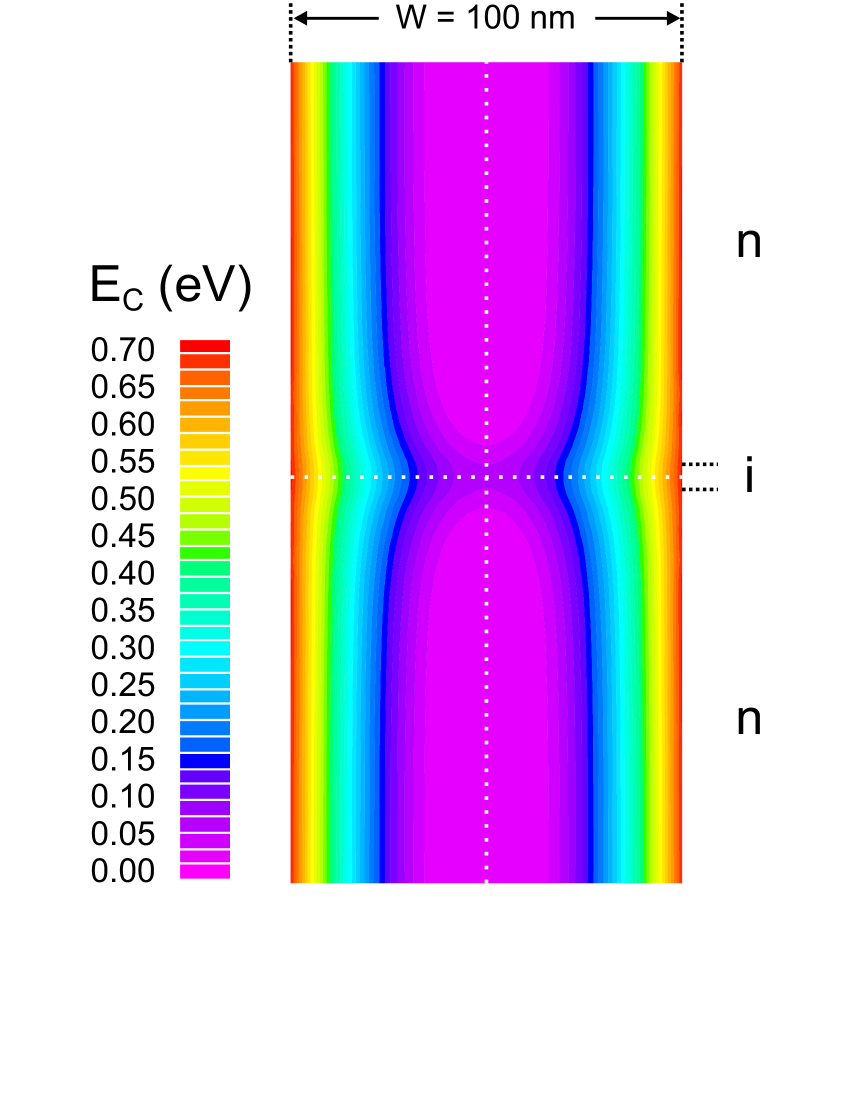
By use of a numerical 3D Poisson-solver Ref_Silvaco for cylindrical symmetry, we have calculated the potential profile within the nanocolumn structure. Fig. 4 visualizes the results as a color map. As an important feature of the system, one can clearly identify the formation of a saddle-point as predicted in Sec. 2. Fig. 5(a) and (b) furthermore show the details of the potential energy within the -plane at and along the center axis at , respectively. (Compare also with Fig. 3.) In turn, a barrier height of meV can be extracted from the simulation. Furthermore, for the curvature of the -potential within the saddle-point we get eVm-2.
In order to compare these values with the expressions of Sec. 2, we invert Eq. (8) and obtain
| (11) |
Inserting the simulated value for , we thus get nm which is in good agreement with nm. Furthermore, employing Eq. (5), we obtain a curvature of eVm-2, which stands in excellent agreement with the result extracted from the simulation above. As for the depletion length, we obtain nm from Eq. (2), which fits very well to the results in Fig. 4 for . The analytical expressions given in Sec. 2 thus represent good approximations for the estimation of the quantum point contact parameters.
Finally, the lateral quantization energy within the quantum point contact given by Eq. (9) reads as meV (the same follows from Eq. (10) with the pinning wavelength nm provided by Eq. (3)). Compared to the energy scale meV at room temperature, we thus can expect a significant impact on the electronic transport properties of a nanodevice based on such a nanocolumn structure at application-relevant temperatures Ref_NL5_2470 .
4 Summary
We have shown how nanoscale doping profiles inside a surface-depleted nanocolumn give rise to the formation of a saddle-point in the potential profile. The obtained lateral confinement varies within the channel direction, resulting in an embedded quantum point contact, which can be the origin of novel collimation transport effects in such nanocolumn structures.
The considered quantum confinement effect is solely due to the formation of a saddle-point in the potential as a special solution of the 3D Poisson equation for a nanoscale intrinsic layer in combination with surface pinning boundary conditions, without the need for any kind of heterostructure. The presented results can be utilized for a new kind of “saddle-point potential engineering” to improve the transport characteristics of quasi-1D nanodevices.
References
- (1) J. Wensorra, K. M. Indlekofer, M. I. Lepsa, A. Förster, and H. Lüth, Nano Letters 5 (2005) 2470.
- (2) M. T. Björk, B. J. Ohlsson, C. Thelander, A. I. Persson, K. Deppert, L. R. Wallenberg, and L. Samuelson, Appl. Phys. Lett. 81 (2002) 4458.
- (3) L. Samuelson, C. Thelander, M. T. Björk, M. Borgström, K. Deppert, K. A. Dick, A. E. Hansen, T. Martensson, N. Panev, A. I. Persson, W. Seifert, N. Skold, L. R. Larsson, and L. R. Wallenberg, Physica E 25 (2004) 313.
- (4) Y. Cui, Z. Zhong, D. Wang, W. Wang, and C. Lieber, Nano Letters 3 (2003) 149.
- (5) R. Calarco, M. Marso, T. Richter, A. I. Aykanat, R. Meijers, A. van der Hart, T. Stoice, and H. Lüth, Nano Letters 5 (2005) 981.
- (6) J. H. Luscombe and C. L. Frenzen, Solid-State Electronics 46 (2002) 885.
- (7) J. A. Hernandes and A. K. T. Assis, J. of Electrostatics 63 (2005) 1115.
- (8) Atlas/Blaze, SILVACO International (2005).