Present address: ]Laboratoire de Spectrométrie Physique, Université Joseph Fourier, Grenoble, France
Transport spectroscopy of a single dopant in a gated silicon nanowire
Abstract
We report on spectroscopy of a single dopant atom in silicon by resonant tunneling between source and drain of a gated nanowire etched from silicon on insulator. The electronic states of this dopant isolated in the channel appear as resonances in the low temperature conductance at energies below the conduction band edge. We observe the two possible charge states successively occupied by spin-up and spin-down electrons under magnetic field. The first resonance is consistent with the binding energy of the neutral state of an arsenic donor. The second resonance shows a reduced charging energy due to the electrostatic coupling of the charged state with electrodes. Excited states and Zeeman splitting under magnetic field present large energies potentially useful to build atomic scale devices.
pacs:
73.21, 73.23, 73.63Dopant atoms are essential in semiconductor technology since they provide extrinsic charges necessary to create devices such as diodes and transistors. Nowadays the size of these electronic devices can be made so small than the discreteness of doping can influence their electrical properties asenov-99-nt . On the other hand it may be an important breakthrough if a dopant could be used as the functional part of a device instead of just providing charges. As an example, dopant-based spin qubits in silicon are possible candidates for quantum computation kane-98-nat ; vrijen-00-pra thanks to their longer spin coherence time tyryshkin-03-prb as compared to two-dimensional quantum dots defined by top gates in III/V heterostructures elzerman-05-review ; petta-05-sci . Although dopants are well known in bulk semiconductors, specific questions arise in the context of nano-scale devices like the reduced life-time of the two-electron state under electric field involved by read-out schemes of spin qubits testolin-05-prb . The aim of this work is to study the electronic states of single dopants in gated silicon nanostructures to bring information useful for these issues.
Electron tunneling through isolated impurities has been observed previously in two-terminal devices such as GaAs/AlGaAs double barrier heterostructures geim-94-prl ; deshpande-96-prl . Here we present experimental results on electron transport through the localized states of individual n-type dopants in silicon nanowires. In contrast to previous studies, our devices have a three-terminal configuration with source, drain, and gate electrodes allowing a detailed investigation of charge, orbital, and spin states. In particular, we observe both the neutral and negatively charged states, and compare their binding energy with the case of bulk dopants. This work provides a quantitative description of the electronic properties of a single dopant connected to electrodes in a gated nanostructure. This is the first transport experiment measuring the charge states of a real atomic system with a attracting Coulomb potential, thus very different from quantum dots with harmonic potentials.

Our devices are 60 nm tall crystalline silicon wires (fins) with large contacts patterned by 193 nm optical lithography and dry etching from Silicon-On-Insulator. After a boron channel implantation, a 100 nm poly-crystalline silicon was deposited on top of a nitrided oxide (1.4 nm equivalent oxide thickness), then received a phosphorus (P) implant as pre-doping, and was patterned using an oxide hard-mask to form a narrow gate (Fig. 1 a,b). Next, we used high-angle arsenic (As) implantations as source/drain extensions, while the channel was protected by the gate and 50 nm wide nitride spacers and remains p-type. Finally, As and P implants and a NiSi metallic silicide are used to complete the source/drain electrodes. Conventional operation of this n-p-n field effect transistor is to apply a positive gate voltage to create an inversion in the channel and allow a current to flow. At low temperature, the sub-threshold conductance shows series of conductance peaks due to electron tunneling through a potential well in the conduction band sellier-06-cm . This well located in the channel is separated from the highly-doped contacts by energy barriers in the access regions due to a poor n-type doping caused by masking silicon nitride spacers next to the gate (Fig. 1b). Here we focus on short devices with 60 nm gate length where the subthreshold regime exhibits specific conductance peaks due to isolated dopants in the channel. All the measurements presented here were gathered on the same sample, but similar features have been observed in other samples of the same length (the width, 385 nm here, is not important because of a corner-effect fossum-03-ieee ; corner-effect ). The experiments were carried out in a dilution fridge at a base temperature of 100 mK. The differential conductance was measured with a lock-in technique using a 50 V amplitude ac voltage.
The energy barrier between source and drain, measured by fitting the thermally activated current at temperatures above 150 K sellier-06-cm , is shown on Fig. 1c. At low gate voltage, when the middle of the channel is the highest point of the potential profile, the barrier height decreases linearly with a coupling . An extrapolation of this linear part to zero barrier shows that the conduction band edge in the channel reaches the Fermi level at 400 mV gate voltage, value above which the low temperature conductance is expected to rise from zero. However, several resonances (a1, b1, a2, b2) are visible at energies below the conduction band edge (inset of Fig. 1c). They come from isolated dopants in the channel and will be analyzed in details throughout the paper. Fig. 1c also show that residual barriers remain at larger gate voltage. Located in the access regions, they create a potential well in the conduction band of the channel, with Coulomb blockade at low temperature as revealed by the conductance peaks c1 and c2.
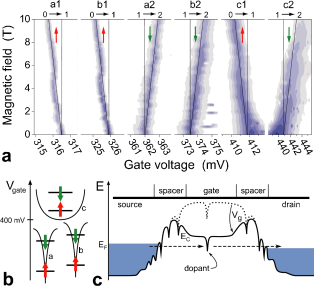
When magnetic field is applied (parallel to the current here), each peak shifts linearly with field (Fig. 2a) and the slopes are consistent with the Zeeman shift of spins having a g-factor of 2 as expected for electrons in silicon (using the conversion factor of each peak as discussed later). Peaks labelled with a 1 (2) correspond to tunneling of spin up (down) electrons under magnetic field. Since the first visible resonances are always of spin up type (also observed in other samples), we conclude that the first peaks (a1 and b1) correspond to tunneling of a first electron () on two different impurities (a and b), and the second set of peaks (a2 and b2) correspond to the second charge state () of each impurity (see Fig. 2b). Note that b1 can not be the second electron of a1 because a two-electron ground state must be a singlet with opposite spins engel-01-prl . Peaks c1 and c2 above the band edge are also respectively spin up and down under magnetic field. They correspond to the first and second electrons of a larger dot (called c) defined electrostatically by the gate in the conduction band profile (Fig. 2c). In this sample, the higher charge states of dot c () are not visible probably due to the progressive loss of Coulomb blockade above 460 mV where the confining barriers disappear. In contrast, in all samples, the impurities like a and b always have exactly two charge states () as expected for dopants because their single positive charge can bind no more than two electrons and with a very small second binding energy hill-77-prl . In addition, the measured Zeeman shifts are experimentally insensitive to the field direction as expected for the 3D Coulomb potential of dopants as opposed to quantum dots in two-dimensional electron gases (2DEG).
Isolated n-type dopants in the p-type channel may come from residual impurities in the SOI layer or from ion implantation of the contacts. Those contributing to the conductance should be close to the gate because of the strong band-bending and along the edges of the wire because this band-bending is stronger due to the corner-effect corner-effect . This strong restriction leads to a silicon volume containing less than one residual donor (considering that p-type silicon should contain less donors than acceptors). The observed isolated donors must therefore arise from the implantation process.

These isolated dopants are atomic-like systems with one or two electrons bound by Coulomb attraction to a central ion and can be characterized by their first and second binding energies. These values are known for dopants in bulk silicon, but we show in the following that we can also measure them in gated nanostructures. Binding energies are related to the gate voltage spacing between the conductance peaks and the conduction band edge located at 400 mV (Fig. 1c). However the energy change on the dopant site is a fraction of the gate voltage spacing, with , , and being the capacitances between the dopant and respectively the source, drain, and gate electrodes. This ratio is determined from the conductance diagram versus gate and bias voltages (Fig. 3b) where positive and negative slopes of conducting sectors equal and (the drain is at ground). We get and for the first peaks (a1 or b1), and and for the second peaks (a2 or b2) probably due to thinner barriers at higher gate voltage. The dopants are therefore well centered in the channel () and mainly coupled to the gate (). The resulting values (a1 or b1) and (a2 or b2) are consistent with the coupling factor determined previously from the gate voltage dependence of the barrier height in the channel below 300 mV. This result validates our assumption that the conduction band in the middle of the channel evolves with the same coupling below and above 300 mV. This point is important since we use it to conclude that the band edge crosses the Fermi level at 400 mV (Fig. 1c) with two dopants below (peaks a1 to b2) and a larger dot above (peaks c1 and c2). In the following we use as an averaged value for the conversion factor.
From the 84 mV (74 mV) spacing between peak a1 (b1) and the band edge, we get 59 meV (52 meV) for the first binding energy of dopant a (b). Since this charge state is neutral, its binding energy is not expected to be modified by the capacitive coupling with the nearby electrodes. For technological reasons, both arsenic and phosphorus dopants are used to make the contacts. Our measured values correspond better to the 54 meV bulk value of arsenic than to the 46 meV of phosphorus ramdas-81-rpp . The small difference between a and b could be related to fluctuations in the band edge energy in the channel, induced for example by disorder at the oxide interface.
The binding energy of the second electron (2 meV only for bulk dopants taniguchi-76-ssc ) is usually very small in this atomic-like system because of a strong repulsive Coulomb interaction called charging energy (52 meV for bulk arsenic dopants). In our case however, since the state is charged, the capacitive coupling with the nearby electrodes is expected to reduce the charging energy to a value where . The 46 mV (48 mV) spacing between peaks a1 and a2 (b1 and b2) indicated on Fig. 3a corresponds indeed to a charging energy between the one-electron and the two-electrons bound states of 32 meV (34 meV) lower than the 52 meV of the bulk. The deduced dopant/gate capacitance F ( F) corresponds to a sphere with 2.7 nm radius in bulk silicon or near a metallic plane covered with a thin layer of silicon dioxide. This radius compares very well with the 2.5 nm Bohr radius of a neutral donor in bulk silicon or with the 3 nm Bohr radius estimated for the negatively charged state norton-76-prl . As a conclusion, the second binding energy of the dopant+gate system is significantly increased by the capacitive coupling, and this effect could provide a longer life-time for the two-electron state involved in the read-out scheme of dopant-based quantum gates.
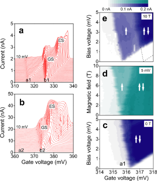
We now turn to the excited state (ES) spectroscopy of the two charge states. In bulk silicon the six-fold valley degeneracy of the conduction band is lifted on a dopant site by the tetragonal symmetry and the first electron ground state (GS) is split into one non-degenerate GS and a few ES all around 12 meV above the GS for phosphorus atoms (22 meV for arsenic) ramdas-81-rpp . An ES of b1 is visible at 5 meV on Fig. 4a as a second current step on top of the GS one. This lower level spacing than expected may originate from the strong band bending and Stark effect near the gate friesen-05-prl which are inherent to these nano-structures. This interesting point will be the object of further investigations. Regarding the two-electrons state, no ES would be observed for a bulk ion since any excitation lies in the continuum hill-77-prl . Here however this charged state is more strongly bound due to the capacitive coupling with the nearby electrodes and several ES can exist. An ES of b2 is indeed clearly visible at 3 meV (Fig. 4b) and has a larger amplitude than the singlet GS in agreement with the triplet degeneracy expected for this first ES with two electrons.
These level spacings of several meV are quite large as compared to 2DEG quantum dots and explain why the quantum regime of Coulomb blockade beenakker-91-prb is observed up to 15 K with conductance peaks increasing for lowering temperature (inset of Fig. 3a, note that at very low temperature the peak width is limited by the escape rate to source and drain). Another consequence of the large level spacing is the absence of level crossing under magnetic field on Fig. 2a because the 1.2 meV Zeeman splitting at 10 T is still smaller than the level spacing. This point is also illustrated on Fig. 4 c, d, e showing the current through the state a1 for a field sweep from 0 to 10 T. The single current step at zero field splits into two steps, the left one corresponding to a flow of spin up electrons and the right one to the sum of spin up and down. The Zeeman splitting at 10 T is given by the bias voltage at which the two spin states contribute and we get 1.2 mV as expected for a spin 1/2 electron in silicon, but here the electron is also bound on a dopant. The dotted lines on Fig. 4e mark the region of the Coulomb-blocked spin down current. The current in the left region is fully polarized with spin up electrons and the dopant acts there as a spin filter. A similar magnetic field behavior has been observed in GaAs/AlGaAs quantum dots hanson-03-prl but with a much lower g-factor than in silicon and with a possible contribution of orbital effects absent in case of dopants.
In conclusion, we used silicon nanowires to investigate the spectrum of single dopants in gated nanostructures. These dopants form attracting Coulomb potentials and induce resonances in the sub-threshold conductance due to electron tunneling through their discrete energy levels. We observed the and charge states, measured their binding energy and the capacitive coupling with nearby electrodes in case of charged states. By means of transport spectroscopy versus bias voltage and magnetic field, we measured the quantum level spacing and Zeeman spin splitting.
We thank F. Koppens and M. Sanquer for useful discussions.
References
- (1) A. Asenov, Nanotechnology 10, 153 (1999).
- (2) B.E. Kane, Nature 393, 133 (1998).
- (3) R. Vrijen et al., Phys. Rev. A 62, 012306 (2000).
- (4) A.M. Tyryshkin et al., Phys. Rev. B 68, 193207 (2003).
- (5) J.M. Elzerman et al., in Lecture Notes in Physics (Springer Berlin / Heidelberg) vol. 667, pp. 25–95 (2005).
- (6) J. Petta et al., Science 309, 2180 (2005).
- (7) M.J. Testolin et al., Phys. Rev. B 72, 195325 (2005).
- (8) A.K. Geim et al., Phys. Rev. Lett. 72, 2061 (1994).
- (9) M.R. Deshpande et al., Phys. Rev. Lett. 76, 1328 (1996).
- (10) H. Sellier et al., cond-mat/0603430.
- (11) J.G. Fossum et al., IEEE Elec. Dev. Lett. 24, 745 (2003).
- (12) Transport is confined to the edges of the silicon wire because the conduction band edge is lower due to a stronger electric field produced by the gate.
- (13) H.-A. Engel and D. Loss, Phys. Rev. Lett. 86, 4648 (2001).
- (14) R.N. Hill, Phys. Rev. Lett. 38, 643 (1977).
- (15) A.K. Ramdas and S. Rodriguez, Rep. Prog. Phys. 44, 1297 (1981).
- (16) M. Taniguchi and S. Narita, Solid State Commun. 20, 131 (1976).
- (17) P. Norton, Phys. Rev. Lett. 37, 164 (1976).
- (18) M. Friesen, Phys. Rev. Lett. 94, 186403 (2005).
- (19) C.W.J. Beenakker, Phys. Rev. B 44, 1646 (1991).
- (20) R. Hanson et al., Phys. Rev. Lett. 91, 196802 (2003).