Transport properties of semiconducting nanocrystal arrays at low temperatures
Abstract
We study the electron transport in semiconducting nanocrystal arrays at temperatures , where is the charging energy for a single grain. In this temperature range the electron transport is dominated by co-tunneling processes. We discuss both elastic and inelastic co-tunneling and show that for semiconducting nanocrystal arrays the inelastic contribution is strongly suppressed at low temperatures. We also compare our results with available experimental data.
Arrays of quantum semiconducting dots, artificial materials with programmable electronic properties, can be tailored to fit many applications ranging from solar cells and elements for energy conversion to generation radiation detectors. Constructing functional electronic devices based on nanocrystals requires understanding their transport properties Yu03 ; tran+prl05 . Electron transport in nanocrystal arrays is governed by the interplay between the internal energy structure of a single nanoparticle and by the strength of inter-particle coupling, i.e by the probability of electron tunneling between neighboring grains. The coupling is quantified by the tunneling conductance BeloborodovRMP , which can be tuned by varying inter-granule distances in fabricated nanocrystal arrays (For review see Collier98 ; Murray00 ).
Each semiconducting nanocrystal is characterized by two energy scales: (i) the mean energy level spacing , where is the density of states at the Fermi surface, is the grain size, and is the dimensionality of a grain, and (ii) the charging energy with being the effective dielectric constant (for a typical grain size of and , are of the order of ). In semiconductors the density of states is of about two orders of magnitude smaller than that in metals. Thus in semiconducting dots the mean energy level spacing, which is inversely proportional to the density of states, can be of order of the charging energy, , in contrast to metallic granular materials where typically .
In this paper we consider transport properties of semiconducting arrays in the limit of weak coupling between the grains, , where is the quantum conductance, and low temperatures . In this temperature regime the electron transport due to sequential tunneling Averin89 , following the activation law , is strongly suppressed. Instead the conductivity of semiconducting nanocrystal arrays is described by the following temperature dependence Philipe04 ; Wehrenberg05 ; Romero05 ; Yakimov03 :
| (1) |
where is the characteristic energy () scale with being the localization length () of the electron trapped on a particular granule remark_xi and a numerical constant of order one. This behavior is identical to the temperature dependent Mott-Efros-Shklovskii variable range hopping (VRH) conductivity in usual bulk semiconductors Shklovskiibook ; Efros .
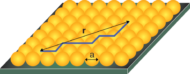
Two remarks are in order: First, this VRH behavior can be observed at temperatures . At temperatures the hopping length becomes of the order of the grain size , see Fig. 1, and Eq. (1) does not hold anymore. Close to , the conductivity follows the simple activation law. Second, Eq. (1) for the conductivity holds also for three dimensional semiconducting nanocrystal arrays and thick granular films with the sample thickness larger than the hopping length .
For the VRH process of Eq. (1) to realize, two ingredients are necessary: first, a finite density of localized states (DOS) on the Fermi surface and second, the mechanism for an electron to tunnel over a distance exceeding the granule size, i.e. a mechanism for a “direct” tunneling through many grains (see Fig. 1). The possible source of a finite DOS in a periodic granular array are charged impurities in the insulating matrix which generate random shifts of the chemical potential of a granule; this was suggested in Ref. [Shklovskii04, ]. The tunneling mechanism mediating VRH was identified as the so-called multiple co-tunneling process in Refs. [Beloborodov05, ; Feigelman05, ], where a theory for VRH in arrays of metallic granules was constructed.
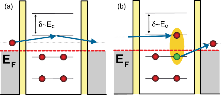
The essence of a co-tunneling process is that an electron tunnels via virtual states in intermediate granules thus bypassing the huge Coulomb barrier. This can be visualized as coherent superposition of two events: tunneling of the electron into a granule and the simultaneous escape of another electron from the same granule. There are two distinct mechanisms of co-tunneling processes, elastic and inelastic co-tunneling Averin90 ; Glazman06 . Elastic co-tunneling means that the electron that leaves the dot has the same energy as the incoming one, Fig. 2 (a). In the event of inelastic co-tunneling, the electron coming out of the dot has a different energy than the entering electron. This energy difference is absorbed by an electron-hole excitation in the granule, which is left behind in the course of the inelastic co-tunneling process, Fig. 2 (b).
The probability for electron tunneling through many grains via elastic or inelastic co-tunneling can be most easily found for the case of the diagonal Coulomb interaction, namely
| (2) |
where is the probability of one elastic/inelastic co-tunneling event through a single grain and is the number of grains, Fig. 1. Below we discuss the probability for elastic and inelastic electron co-tunneling separately and derive expressions for the corresponding localization length , which is defined by . In terms of the amplitude for an electron tunneling through a grain the probability can be expressed as , where the symbol denotes the averaging over randomness in the system.
Semiconducting nanocrystal arrays are described by the Hamiltonian
| (3) |
where are the grain indexes and summation in the second term of the r.h.s. of Eq. (3) is performed over nearest neighbors. The term stands for electrons in the single grain , and is the tunneling Hamiltonian between the adjacent grains and
| (4) |
Here are the random tunneling matrix elements and [] is the creation [annihilation] operator on the th grain. The symbol ′ at the sum is to reflect that due to the large mean level spacing in semiconducting grains , only a few terms of the sum are important.
Elastic co-tunneling.— First we discuss the conductivity of semiconducting nanocrystal arrays due to elastic co-tunneling, Fig. 2 (a). In order to derived the probability for such a process, we calculate the related amplitude for the elemental elastic co-tunneling process which is in general given by ; the energies are differences of energy levels of adjacent grains. Averaging over the random tunneling matrix elements, we obtain for the amplitude probability density the following expression
| (5) |
where is the inverse electron escape time from a grain and we used Gaussian distributed tunneling matrix elements remark_distr , . Since for semiconducting grains the mean level spacing is of the order of [remark_sum, ], we obtain for the elastic localization length , using Eqs. (2), (5), the following expression
| (6) |
For one has to take into account all terms of the sum in (5) leading to a different power of the logarithm in the denominator of (6). Therefore it follows that for the localization length of semiconducting nanocrystal arrays is smaller than the localization length in metallic arrays if the grain size and dielectric constant, i.e. , are the same Beloborodov05 ; BeloborodovRMP .
Inelastic co-tunneling.—Next, we discuss the contribution to the conductivity of a semiconducting nanocrystal array due to inelastic co-tunneling processes, Fig. 2 (b). In contrast to the elastic process the amplitude has an exponential dependence on the mean level spacing, , which reflects the fact that the smallest energy of an electron-hole pair is of the order of mean energy level spacing in a grain. The amplitude probability density for an inelastic co-tunneling process has therefore the form
| (7) |
For high temperatures, , the numerator approaches unity. For the inelastic localization length we obtain
| (8) |
For temperatures , the last term in the denominator of Eq. (8) is the dominant one. In this case the localization length reduces to
| (9) |
Comparing Eqs. (6) and (9) one can see that at low temperatures, meaning that inelastic processes are strongly suppressed and therefore the main mechanism for conductivity is elastic co-tunneling.
Discussion.—As we have shown, the inelastic co-tunneling process is suppressed in semiconducting nanocrystal arrays. This can also be seen by comparing the crossover temperatures separating the elastic and inelastic mechanisms of electron co-tunneling in the metallic and semiconducting case. For metallic granular arrays this is of the order of [Averin90, ; BeloborodovRMP, ; Feigelman05, ], where the mean level spacing is small. In the case of semiconducting nanocrystal arrays is of the order of the charging energy, , therefore the crossover temperature is of the order of , i.e., much larger than the temperature such that at low temperatures inelastic co-tunneling does not contribute to the transport.
If the applied electric field grows sufficiently high, , the hopping conductivity becomes field-dependent: , where and , in full analogy with the Shklovskii result Shklovskii73 for hopping conductivity in usual bulk semiconductors in a strong electric field.
As a last remark, we would like to discuss the possibility of the observation of the Mott law in semiconducting nanocrystal arrays. In usual (bulk) semiconductors, the Efros-Shklovskii law may turn into the Mott behavior with the increase of temperature. This happens when the typical electron energy involved in a hopping process becomes larger than the width of the Coulomb gap , i.e. when it falls into the flat region of the density of states where Mott behavior is expected. To estimate the width of the Coulomb gap, , one compares the Efros-Shklovskii expression for the density of states
| (10) |
with the DOS in the absences of the long-range part of the Coulomb interactions, . Using the condition we obtain
| (11) |
Inserting the value for the bare DOS, , into Eq. (11) we finally obtain
| (12) |
Equation (12) means that there is no flat region in the density of ground states and, thus, the Mott regime is difficult to observe in semiconducting nanocrystal arrays.
Recent experiments on semiconducting nanocrystal materials, CdSe, PbSe, and GeSi, revealed the VRH conductivity Philipe04 ; Wehrenberg05 ; Romero05 ; Yakimov03 . The results allow for determining the characteristic energy scale and/or field . These scales are related via . Using our results for the localization length (6) in connection with the definition of both energy scales, e.g., the mean grain size can be calculated, i.e., represents an alternative to direct measurements with, e.g. a scanning tunneling microscope. As an example we reexamine the results of Ref. [Philipe04, ] for CdSe nanocrystal arrays which were measured in the low and high electric field regime: was measured to be which gives together with a localization length . Using their value for gives . Due to the logarithm in (6), the localization length is of the order of the grain size () and therefore our estimates are also in agreement with their directly observed size of .
In conclusion, we have discussed transport properties of semiconducting nanocrystal arrays at low temperatures. We have shown that the electron transport is dominated by co-tunneling processes and for temperatures the main mechanism for electron tunneling through many grains is the elastic electron co-tunneling. Our results for the localization length can be used to extract information about the morphology of the sample, e.g., the average grain size, without direct measurements.
Acknowledgements.—We thank Philippe Guyot-Sionnest and Andrei Lopatin for useful discussions. A.G. acknowledges support by the DFG through a research grant. This work was partly supported by the U.S. Department of Energy Office of Science through contract No. DE-AC02-06CH11357.
References
- (1) D. Yu, C. Wang, and P. Guyot-Sionnest, Science 300, 1277 (2003).
- (2) T. B. Tran, I. S. Beloborodov, X. M. Lin, T. P. Bigioni, V. M. Vinokur, and H. M. Jaeger, Phys. Rev. Lett. 95, 076806 (2005).
- (3) I. S. Beloborodov, K. B. Efetov, A. Lopatin, and V. M. Vinokur, cond-mat/0603522 (to be published in Rev. Mod. Phys.).
- (4) C. Collier, T. Vossmeyer, and J. Heath, Annual review of Physical Chemistry 49, 371 (1998).
- (5) C. Murray, C. Kagan, and M. Bawendi, Annual review of Materials Science 30, 545 (2000).
- (6) D. V. Averin and A. A. Odintsov, Phys. Lett. A 140, 251 (1989).
- (7) D. Yu, C. J. Wang, B. L. Wehrenberg, and P. Guyot- Sionnest, Phys. Rev. Lett. 92, 216802 (2004).
- (8) B. L. Wehrenberg, D. Yu, J. Ma, and P. Guyot-Sionnest, J. Phys. Chem. B 109, 20192 (2005).
- (9) H. Romero and M. Drndic, Phys. Rev. Lett. 95, 156801 (2005).
- (10) A. I. Yakimov, A. V. Dvurechenskii, A. V. Nenashev, and A. I. Nikiforov, Phys. Rev. B 68, 205310 (2003).
- (11) On length scales well exceeding the grain size (for example on the scale of the hopping length) the behavior of the semiconducting nanocrystal array is similar to that of bulk semiconductors.
- (12) B. I. Shklovskii and A. L. Efros, Electronic properties of Doped Semiconductors, Springer-Verlag, New York, 1988.
- (13) A. L. Efros and B. I. Shklovskii, J. Phys. C 8, L49 (1975).
- (14) J. Zhang and B. I. Shklovskii, Phys. Rev. B 70, 115317 (2004).
- (15) M. V. Feigel’man and A. S. Ioselevich, Pis ma Zh. Eksp. Teor. Fiz. 81, 341 (2005) [Sov. Phys. JETP Lett. 81, 227 (2005)].
- (16) I. S. Beloborodov, A. Lopatin, and V. Vinokur, Phys. Rev. B 72, 125121 (2005).
- (17) D. Averin and Yu. Nazarov, Phys. Rev. Lett. 65, 2446 (1990).
- (18) L. Glazman and M. Pustilnik. cond-mat/0501007
- (19) For our considerations the assumption of a Gaussian distribution of the tunneling matrix elements is not crucial, since a different distribution will only change the expression for the electron escape time and therefore the qualitative picture for the localization length remains the same.
- (20) Eq. (6) is valid also if is slightly smaller than . Only in this case one can take into account only a few terms in the summation over the states in Eq. (5) in order to derive Eq. (6). If the grains are metallic Eq. (6) is still valid as long as the grain size is very small such that is of order .
- (21) B. I. Shklovskii, Fiz. Tekh. Poluprovodn. (S.-Petersburg) 6, 2335 (1973) [Sov. Phys. Semicond. 6,1964 (1973)].