Microwave photoresistance of a high-mobility two-dimensional electron gas in a triangular antidot lattice
Abstract
The microwave (MW) photoresistance has been measured on a high-mobility two-dimensional electron gas patterned with a shallow triangular antidot lattice, where both the MW-induced resistance oscillations (MIRO) and magnetoplasmon (MP) resonance are observed superposing on sharp commensurate geometrical resonance (GR). Analysis shows that the MIRO, MP, and GR are decoupled from each other in these experiments.
pacs:
73.40.-c, 73.21.-b, 72.40.+wThe subject of electronic transport in a high-mobility two-dimensional electron gas (2DEG) under microwave (MW) irradiation (frequency ) and a small magnetic field () has attracted much recent attention, largely because of the spectacular microwave-induced magneto-resistance oscillations 1 (MIRO) and the subsequent zero-resistance states (ZRS) observed in very clean samples.2 ; 3 ; 4 ; 5 ; 6 ; 7 The period (in 1/) of MIRO is controlled by a ratio between the and the cyclotron frequency, . To a large extent, present theoretical models proposed to explain the MIRO are focused on the displacement of electrical currents by random scatters,8 ; 9 or on the electron distribution function modulated by the presence of microwaves.10 These models are able to explain the observed large amplitude oscillations, and suggest that in very clean samples and under sufficient microwave power, the 2DEG can exhibit absolute negative conductivity (ANC). The ZRS arise 11 because in the ANC regime, the system reaches an instability against the formation of current domains, and the measured voltage in a macroscopic sample vanishes. Other models which do not invoke ANC include those based on orbital dynamics 12 ; 13 or coherent interference effect.14
The MIRO and ZRS in a modulated 2DEG has been studied in recent theoretical work.15 ; 16 In particular, for one-dimensional (1D) modulation,15 the displacement model8 ; 9 and the distribution model10 are found to contribute to MIRO in an anisotropic manner. In principle, experiments in such a system can help to distinguish the relative contributions from each mechanism. For 2D modulation,16 different features can be expected on an ultraclean 2DEG. Moreover, a periodical modulation breaks translational symmetry of the 2DEG allowing studies of photoresistance with a finite momentum transfer in this system.
In this paper we report on an experimental study of MW photoresistance in a 2D periodically modulated 2DEG. The MIRO are observed in a triangular antidotes array patterned in a high-mobility GaAs/AlxGa1-xAs heterojunction. The MIRO retain a 1/ periodicity as in unpatterned 2DEG, but their amplitude is strongly damped. We also found the photoresistance peaks corresponding to long-wavelength magnetoplasmon (MP) resonance; the dispersion of MP is controlled by the width of the Hall bar rather than the period of potential modulation. We conclude that the MIRO, MP, and DC geometric resonance (GR) are decoupled from each other in these experiments. While MW photoconductivity has been reported for antidot arrays in a modest-mobility 2DEG,17 our work on a high-mobility system reveals different features, including MIRO, and opens a new window for studies of nonequilibrum quantum transport.
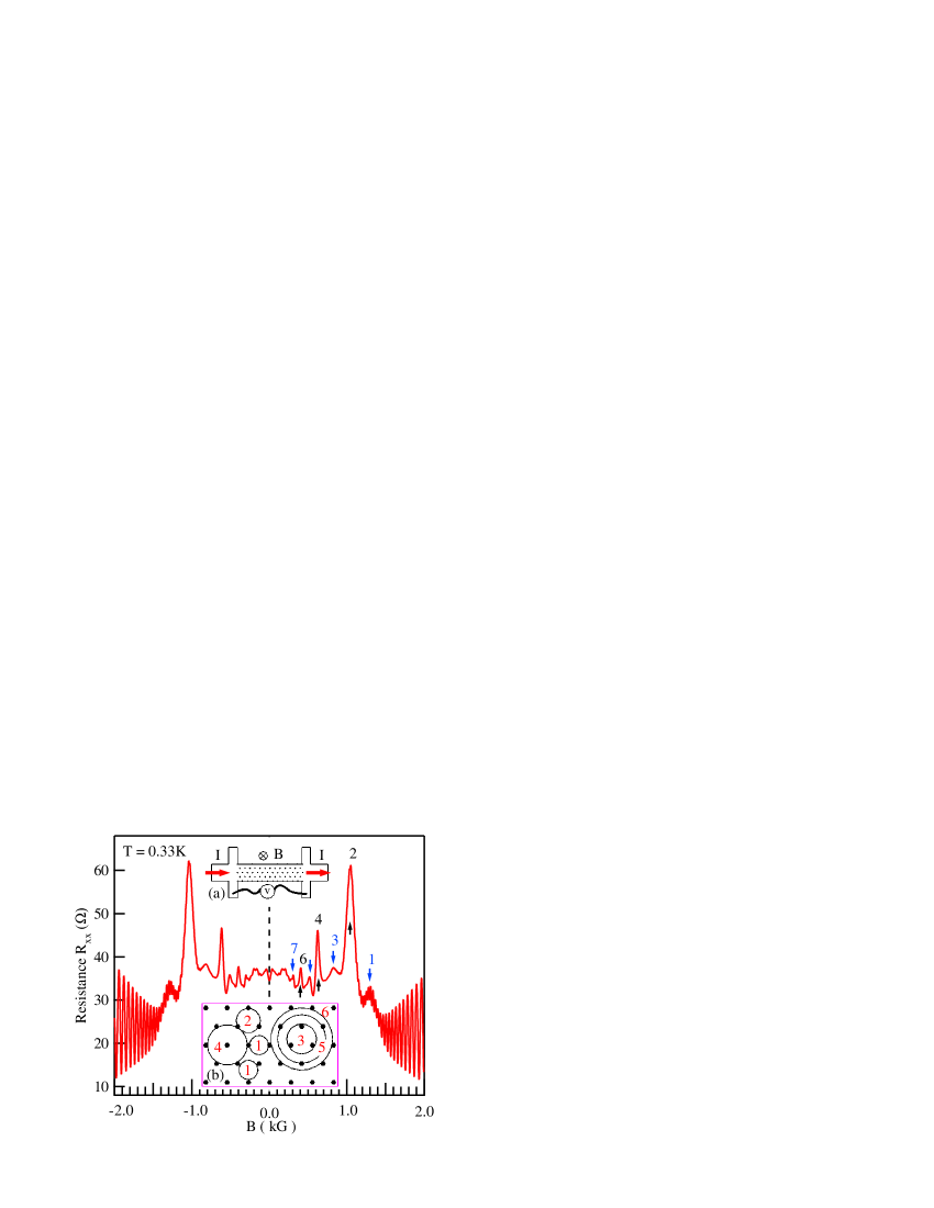
Our 2DEG is cleaved from a high-mobility GaAs/Al0.3Ga0.7As heterostructure wafer grown by molecular beam epitaxy, with a K mobility 107 cm2/V s before processing. An 80-m-wide, 320-m-long Hall bar was first defined on the sample by optical lithography and wet etching, then a triangular antidot lattice, with period nm and dot diameter = 300 nm, was patterned on the Hall bar through -beam lithography and reactive ion etching [see inset (a) in Fig. 1]. After the processing, the 2DEG has an electron density cm-2 and a mobility cm2/V s . Such parameters were obtained after a brief illumination from a red light-emitting diode at = 4 K. Note that the introduction of antidot lattice reduced the mobility four fold. However, the transport mean free path, 22 m, where is the electron-effective mass and is the Fermi velocity, exceeds the period by at least one order of magnitude, indicating a much cleaner system than previously reported.17 ; 18 ; 19
Our measurement was performed in a 3He refrigerator equipped with a superconducting magnet. The MW was supplied by a set of Gunn diodes and sent via a waveguide to the sample immersed in the 3He coolant. The mutual orientation of the waveguide, sample, and the magnetic field corresponds to Faraday configuration; the excitation current flows perpendicularly to the microwave polarization. The magnetoresisitance was measured with a standard low-frequency lock-in technique (frequency 23 Hz and excitation current 1 A).
To characterize the sample, at first we measured its magnetoresistance without MW irradiation. A trace is shown in Fig. 1, in which a set of sharp peaks were resolved and are attributed to geometrical resonance. In magnetoresistance, GR occurs whenever the cyclotron radius becomes commensurate with the period a of the artificial scatterers,18 ; 19 i.e.,
| (1) |
where is a constant depending on the geometry of the artificial periodic scatterers, and with is the magnetic length and is the Fermi wave vector of the 2DEG. Note that is satisfied in the magnetic-field regime of all these peaks, where is the momentum relaxation time determined by mobility, thus a full cyclotron orbit can be completed between the scattering events.
The observed GR (Fig. 1) are much sharper than previously reported18 ; 19 and up to seven distinct resistance peaks are clearly resolved, attesting to the extraordinary quality of the sample. Remarkably, the GR peaks exhibit an alternating strength in a sweep, with the “even” peaks (i.e., 2,4,6) standing out as compared to the “odd” peaks (1,3,5,7). Moreover, the peak position in does not conform to the set of ratio in previous reports.18 ; 19 For example, according to Ref. 19, , the strongest peak occurs at corresponding to a first-pinned semiclassical orbit in a triangular lattice of period a, whereas in Fig. 1 the strongest peak (labeled by 2) occurs at . A similar observation can be found for the second-strongest peak (4 in Fig. 1), where is found to shift from 0.85 to 0.94 in the present case. The 10% increase of the ratio indicates that in high-mobility samples, major resistance peaks may not correspond to pinned orbits. Rather, they correspond to those commensurate orbits, which dynamically experience most frequent scattering events, and hence higher conductance. Since in our high-mobility sample the GR occur in the regime , and so, , these states give rise to the high-resistance peaks in the Hall bar geometry. This scenario requires that the electron orbit of radius be scattered sequentially by multiple antidots. The orbital dynamics described here is equivalent to the theoretically studied runaway trajectories of delocalized electrons skipping from one antidot to another.19b ; 19c These orbits are drawn schematically in inset (b) of Fig. 1. The exceptional sharpness of the peak can be attributed to the small ratio of in the present sample.
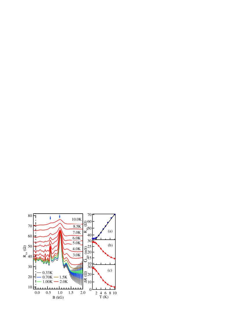
Our temperature-dependent measurements show that the major resistance peaks (2,4,6) persist up to above 10 K whereas the minor peaks (1,3,5) essentially diminish at 6 K. From these temperature dependences, we can roughly estimate the height of antidot potential for the electron orbits involved, which is much less than the Fermi energy of the 2DEG (100 K).
Temperature dependence of the GR was measured from = 0.33 to 10 K; the results are shown in Fig. 2. At K, the amplitude of the GR shows very little change with temperature, while the Shubnikov-de Haas oscillations dampen quickly with increasing temperature. At K, the GR peaks are greatly damped by raising the temperature. This is clearly depicted in inset (c) of Fig. 2. This temperature dependence is consistent with the dominance of thermally excited phonon scattering at this temperature range,20 rather than the mechanism of smearing of Fermi surface21 typically taking place at 100 K. Interestingly, this behavior is similar to the temperature dependence of the = 0 conductance [inset (b)], which is characteristic for the thermally excited phonon scattering model.20 From insets (a), (b), and (c), we can see that this regime transition happens at about 2 K.
In the rest of the paper we shall report on photoresistance on the patterned 2DEG sample, where the photoresistance is defined as the change of resistance due to MW irradiation: , and being the magnetoresistance with or without MW irradiation, respectively. As an example, Fig. 3(a) shows traces with and without continuous MW irradiation at = 56 GHz. In this measurement, the lattice temperature was kept at K.
trace with MW irradiation looks quite complicated because GR and MW-induced oscillations overlap in this low magnetic field regime. And as can be seen, the GR dominate this regime and make the MW-induced oscillation difficult to resolve. Our analysis shows that under MW irradiation, both the electron-heating effect and MIRO contribute to the of the patterned 2DEG. The heating effect originates from the strong dependence of GR peaks in the temperature range 1.5 K, as presented earlier. Since GR peaks exhibit a negative temperature coefficient, , electron heating results in a reduction of in the sample. Our main purpose in this experiment is to recover the photoresistance from the background of the electron-heating signal.
It is possible to deduce the by numerically substracting from , as shown by the dotted line in Fig. 3(b). The obtained in this way shows an oscillatory structure roughly periodical in 1/, similar to the MIOR observed in unpatterned 2DEG. On the other hand, significant distortion of the can be anticipated owning to the contribution from the electron heating effect. While both the and data were taken at approximately the same lattice temperature 1 K, the electron temperature is expected to be considerably higher in , leading to a large heating component.
The can also be measured directly by a double modulation technique22 in the following fashion. The MW was chopped at a frequency = 11.5 Hz, and the sample excitation current is synchronized at the double frequency 2 = 23 Hz. Using the frequency as a lock-in reference, it can be shown that the can be attained from the lock-in signal.22 The at the same MW frequency 56 GHz, measured with a double-modulation method, is shown in Fig. 3(b). We note that the obtained by both methods coincide reasonably well in their oscillatory structure in , indicating the equivalence of these two methods in obtaining the .
The following observations can be made for the MIRO in a modulated 2DEG, as measured here, in comparision to the MIRO in an unpatterned 2DEG.1 First, the MIRO in modulated 2DEG retain the characteristic period in determined by = /. Second, the damping of MIRO is much steeper in the modulated sample even though the mobility is comparable. The mobility of the unpatterned sample in Ref. 1, is about cm2/V s, where up to ten MIRO peaks can be observed, whereas in the present sample of a mobility cm2/V s, only two peaks are clearly resolved. Of course, mobility is directly proportional to the transport lifetime , which is only relevant at = 0. In a small magnetic field, the electron orbital dynamics are strongly influenced by the modulation. The above observations may point to an interesting theoretical question as to how such a modulation will affect the electrical current distribution in the MIRO regime. On a side note, our results could also support the notion that MIRO is a bulk, rather than an edge, effect.

Using the double-modulation method, we have measured the MIRO in a wide range of frequencies between 32 and 130 GHz, and qualitatively the same conclusion can be drawn throughout this range: MIRO can be clearly observed in a 2DEG with a shallow triangular antidots modulation, but with strongly damped amplitude.
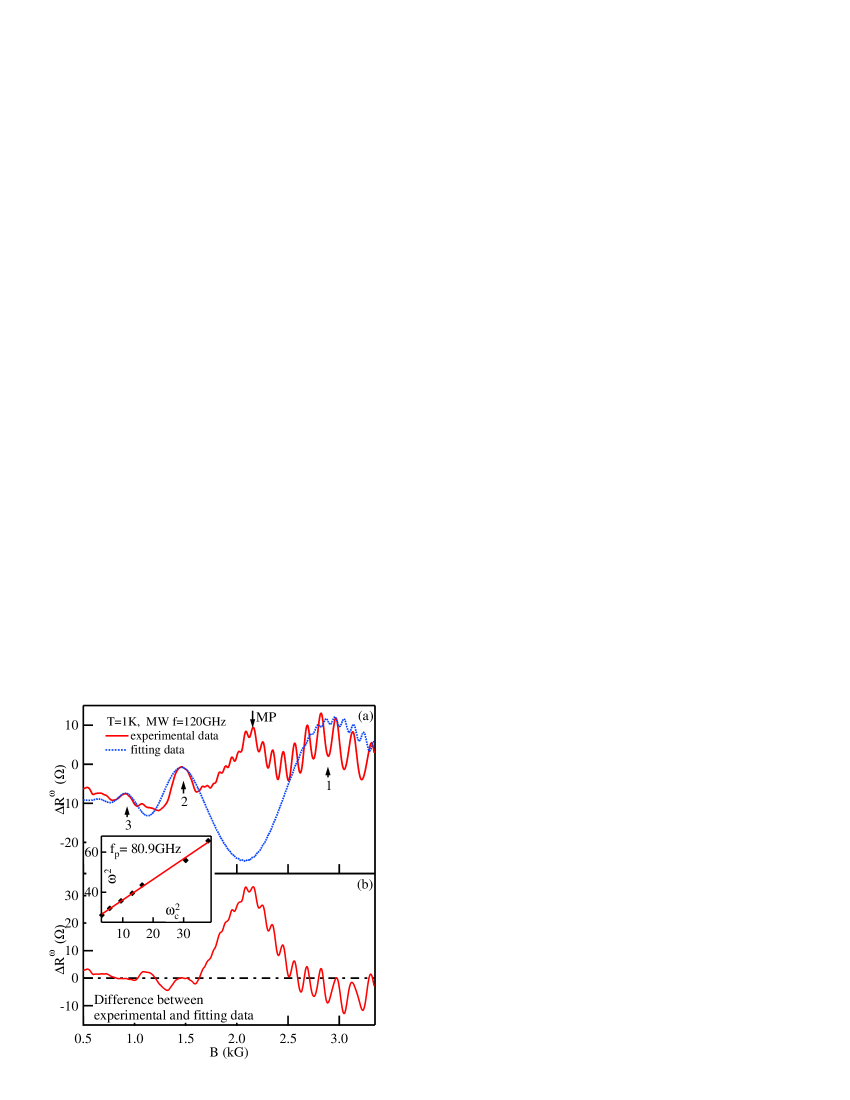
We observed an additional single resistance peak in the high-frequency regime, 85 GHz, and identified it as the signal of magnetoplasmon resonance.1 ; 23 Since the MIRO and MP resistances are superposed, we rely on the following empirical procedure to extract the MP signal.
It is shown empirically in Ref. 24, that the periodicity and the shape of in the MIRO can be reasonably fitted by a model based on the oscillatory electron distribution function at a given temperature , with the Landau level width being a fitting parameter. In Fig. 4, we fit the 120 GHz experimental (solid line) with a calculated curve (dotted line). Both the zero line and the amplitude of the curve were adjusted such that the envelops of both coincide. From the fit we obtain a width of 56 eV 0.65 K, corresponding to a scattering time of 12 ps. It is interesting to compare the fitted in the MIRO of unpatterned 2DEG from the same wafer, which is 41 eV (16 ps).
Subtracting the fitting curve from the experimental trace, we arrive at a trace which is dominated by a strong MP peak. For 2DEG, the magnetoplasmon resonance shall occur at
| (2) |
where is the MW frequency, is the cyclotron frequency, and is the 2D plasmon frequency, which is given by23
| (3) |
where wave vector with w the lateral width of 2DEG. The relation of Eq. (3) is well revealed in the inset of Fig. 4, and a fitting gives a 2D plasmon frequency of 80.9 GHz. For our GaAs sample, taking into account the fact that the 2DEG is very close to the surface, the effective dielectric constant is 6.9.23 Using and the width of Hall bar is 80 m , with formula (3) we arrive at a 2D plasmon frequency 98 GHz, which is about 20% larger than the measured one.
In summary, we have experimentally studied the microwave photoresistance in a high-mobility 2DEG modulated by a 2D triangular potential. The geometric resonance observed in the sample is remarkably different from previous systems of lower mobility. We observed microwave-induced resistance oscillations and magnetoplasmon resonance that are characteristically similar to those of unpatterned 2DEG. Present data shows that MIRO, MP, and geometric resonance are essentially decoupled from each other in these experiments. Ultimately, one would like to pursue the experimental regime where periodical modulation would lead to characteristically new behavior in the MIRO and ZRS. Along this line, a clean 2D electron system consisting of a short modulation period approaching magnetic length would offer exciting opportunities. Finally, the issue concerning scattering parameters and their influences in the microwave photoresistance remains open for experimental as well as theoretical work.
We thank K. Stone for technical assistance in the experimental work and D. Wu, and N. Zheng for sample fabrication. This work was supported by contract No. NSF-DMR 0408671.
References
- (1) M. A. Zudov, R. R. Du, J. A. Simmons, and J. L. Reno, Phys. Rev. B 64, 201311(R) (2001).
- (2) R. G. Mani, J. H. Smet, K. von Klitzing, V. Narayanamuri, W. B. Johnson, and V.Umansky, Nature 420, 646 (2002).
- (3) M. A. Zudov, R. R. Du, L. N. Pfeiffer, and K. W. West, Phys. Rev. Lett. 90, 046807 (2003); C. L. Yang, M. A. Zudov, T. A. Knuuttila, R. R. Du, L. N. Pfeiffer, and K. W. West, ibid. 91, 096803 (2003).
- (4) S. I. Dorozhkin, JETP Lett. 77, 577 (2003).
- (5) R. L. Willett, L. N. Pfeiffer, and K. W. West, Phys. Rev. Lett. 93, 026804 (2004).
- (6) S. A. Studenikin, M. Potemski, P. T. Coleridge, A. S. Sachrajda, and Z. R. Wasilewski, Solid State Commun. 129, 341 (2004).
- (7) For an incomplete list of references prior to 2004, see, e.g., R. R. Du, M. A. Zudov, C. L. Yang, L. N. Pfeiffer, and K. W. West, Physica E 22, 7 (2004); M. G. Vavilov and I. L. Aleiner, Phys. Rev. B 69, 035303 (2004).
- (8) A. C. Durst, S. Sachdev, N. Read, and S. M. Girvin, Phys. Rev. Lett. 91, 086803 (2003); J. Shi and X. C. Xie, ibid. 91, 086801 (2003); X. L. Lei and S. Y. Liu, ibid. 91, 226805 (2003).
- (9) V. I. Ryzhii, Sov. Phys. Solid State 11, 2078 (1970).
- (10) I. A. Dmitriev, M. G. Vavilov, I. L. Aleiner, A. D. Mirlin, and D. G. Polyakov, Phys. Rev. B 71, 115316 (2005).
- (11) A. V. Andreev, I.L. Aleiner, and A.J. Millis, Phys. Rev. Lett. 91, 056803 (2003).
- (12) J. C. Phillips, Solid State Commun. 127, 233 (2003).
- (13) J. Inarrea and G. Platero, Phys. Rev. Lett. 94, 016806 (2005).
- (14) D. H. Lee and J. M. Leinaas, Phys. Rev. B 69, 115336 (2004).
- (15) J. Dietel, L. I. Glazman, F. W. J. Hekking and F. von Oppen, Phys. Rev. B 71, 045329 (2005).
- (16) M. Torres, and A. Kunold, J. Phys.: Condens. Matter. 18, 4029 (2006).
- (17) E. Vasiliadou, R. Fleischmann, D. Weiss, D. Heitmann, K. von. Klitzing, T. Geisel, R. Bergmann, H. Schweizer, and C. T. Foxon, Phys. Rev. B 52, R8658 (1995).
- (18) D. Weiss, M. L. Roukes, A. Menschig, P. Grambow, K. von Klitzing, and G. Weimann, Phys. Rev. Lett. 66, 2790 (1991).
- (19) T. Yamashiro, J. Takahara, Y. Takagaki, K. Gamo, S. Namba, S. Takaoka, and K. Murase, Solid State Commun. 79, 885 (1991).
- (20) E. M. Baskin, G. M. Gusev, Z. D. Kvon, A. G. Pogosov, and M. V. Entin, JETP Lett. 55, 678 (1992).
- (21) Mesoscopic Physics And Electronics, edited by T. Ando et al. (Springer-Verlag, Berlin, 1998), Chap. 2.5, pp.72-76.
- (22) J. Zhang, S. K. Lyo, R. R. Du, J. A. Simmons, and J. L. Reno, Phys. Rev. Lett. 92, 156802 (2004).
- (23) P. H. Beton, P. C. Main, M. Davison, M. Dellow, R. P. Taylor, E. S. Alves and L. Eaves, S. P. Beaumont, and C. D. W. Wilkinson, Phys. Rev. B 42, 9689 (1990).
- (24) M. A. Zudov, Ph.D. thesis, University of Utah, 1999.
- (25) E. Vasiliadou, G. Muller, D. Heitmann, D. Weiss, K. von. Klitzing, H. Nickel, W. Schlapp, and R. Losch, Phys. Rev. B 48, 17145 (1993).
- (26) S. A. Studenikin, M. Potemski, A. Sachrajda, M. Hilke, L. N. Pfeiffer, and K. W. West, Phys. Rev. B 71, 245313 (2005).