Influence of the inhomogeneous field at the tip
on quantitative piezoresponse force microscopy
Abstract
Ferroelectric domain imaging with piezoresponse force microscopy (PFM) relies on the converse piezoelectric effect: a voltage applied to the sample leads to mechanical deformations. In case of PFM one electrode is realized by the tip, therefore generating a strongly inhomogeneous electric field distribution inside the sample which reaches values up to V/m directly underneath the apex of the tip. Although often assumed, this high electric field does not lead to an enhancement of the piezoelectric deformation of the sample. On the contrary, internal clamping of the material reduces the observed deformation compared to the theoretically expected value which depends only on the voltage thus being independent of the exact field distribution.
pacs:
77.80.Dj, 68.37.Ps, 77.84.-sFerroelectric domain patterns are the basis of a multitude of applications such as quasi-phase-matched frequency converters Fej92 , electro-optic scanners Gah01 , nonlinear photonic crystals Bro00 , and ultra-high density data storage devices Cho05 . For further improvement of the domain patterns their visualization with high lateral resolution is indispensable. Although several techniques have been developed Soe05 , piezoresponse force microscopy (PFM) has become a standard technique in recent years mainly because of its easy use. However, the interpretation of the obtained images is still challenging, therefore quantitative data is published very rarely. This deficiency is often justified by the presumption that due to the strong dependency of the electric field on the tip radius, which in general is not known exactly, a quantitative analysis of the data is not possible. Arguing that way, however, ignores the fact that, at least in a first approximation, not the electric field distribution but only the applied voltage determines the piezoelectric deformation of the sample. Although this statement is self-evident from theoretical considerations, we carried out experiments with different single-domain crystals, comparing the measured deformation underneath the tip with and without an additional top electrode.
PFM is based on the deformation of the sample due to the converse piezoelectric effect. The piezoresponse force microscope is a scanning force microscope (SFM) operated in contact mode with an additional alternating voltage applied to the tip. In piezoelectric samples this voltage causes thickness changes and therefore vibrations of the surface which lead to oscillations of the cantilever that can be read out with a lock-in amplifier. In ferroelectric samples different orientations of the polar axis of adjacent domains lead to a domain contrast, i. e., the domain faces are displayed as bright or dark areas in PFM images (an overview of the PFM technique can be found in Alexe ). The generally observed frequency dependence of those measurements Agr05 ; Scr05 ; Lab00 was recently be explained by a system-inherent background Jun05a . We also proposed a detection scheme that allows a straight forward quantitative analysis of the obtained data Jun05b . In this contribution we investigate the influence of the strongly inhomogeneous electric field of the tip on the piezoelectric deformation measured with PFM.
The (longitudinal) converse piezoelectric effect says that in an external electric field a piezoelectric material of thickness undergoes a thickness change proportional to the appropriate piezoelectric coefficient :
| (1) |
Note that the thickness change does not depend on the thickness of the sample but only on the applied voltage . That is why for piezoelectric transducer elements, not thick crystals but stacks of multiple piezoelectric discs, all of them connected individually, are utilized piezo .
In case of PFM the electric field is generated by the tip and a large homogeneous back electrode. Typical dimensions are: tip radius nm, thickness of the crystal several 100 µm, and back electrode some mm2. The voltage applied between tip and back electrode usually is 10 – 20 Vpp which leads to electric field strength at the very tip of the order of V/m (for nm and V). Assume a coordinate system such that the -axis is perpendicular to the surface of the sample under investigation (thus lies in the symmetry axis of the tip). Because the electric field has a radial symmetry, piezomechanical deformations due to field components perpendicular to cancel out at the position of the tip apex. The electric field relevant for PFM measurements can therefore be reduced to . Equation (1) is also valid if the electric field is not homogeneous along the sample thickness because . Therefore the inhomogeneous distribution of the electric field underneath the tip has no effect on the piezoelectric deformation along the direction.
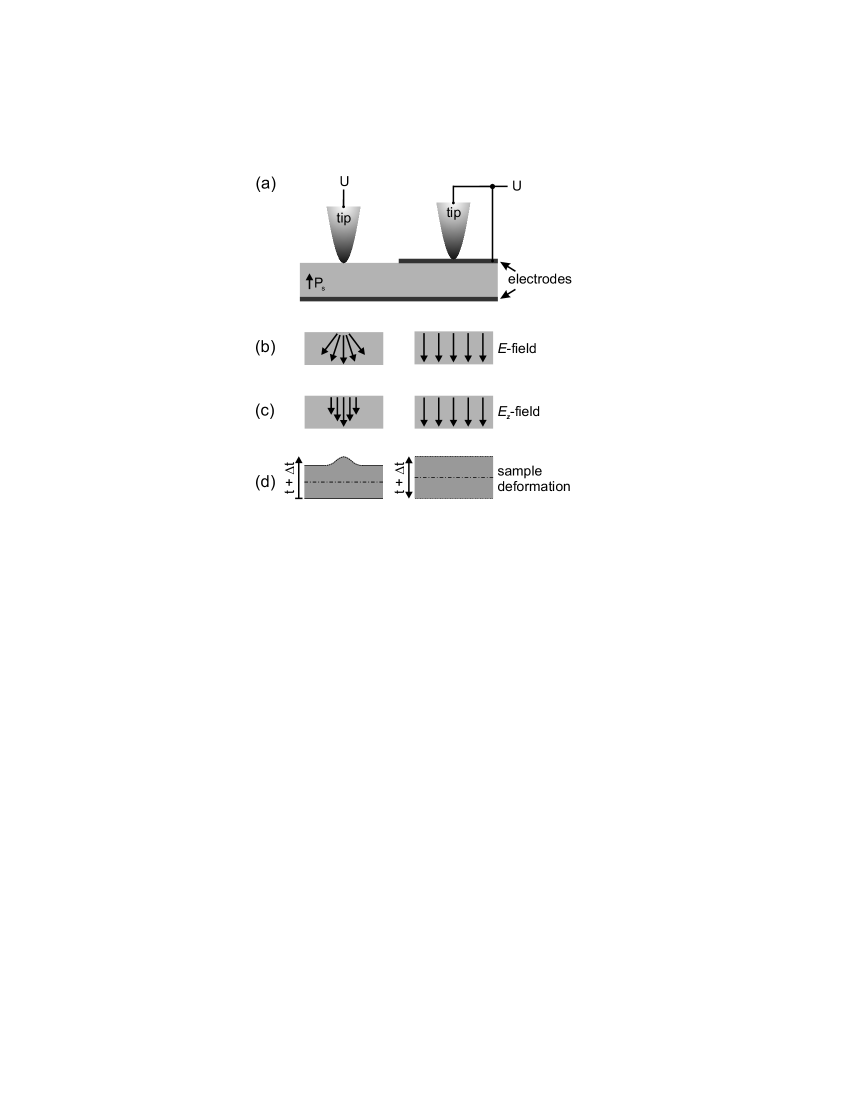
In order to support this statement we prepared samples of different single crystals where part of the topface was covered with a conductive, 50 nm thick gold-layer of 10 mm2 area, the backside being fully covered with a gold layer to ensure a homogeneous back electrode (Fig. 1(a)). In case of the PFM tip acting as electrode the field distribution is strongly inhomogeneous whereas with the large gold electrode a homogeneous field inside the crystal is generated (b). In (c) the relevant electric field component is depicted. The expected deformations are schematically shown in (d). In case of a homogeneous field (right side) the whole volume of the sample undergoes a thickness change whereas in case of the tip acting as an electrode, the deformation occurs only in a restricted volume at the very surface of the crystal.
For PFM measurements a frequency of 10 - 100 kHz usually is chosen for the alternating voltage applied to the tip. With the tip acting as electrode, the generally observed frequency dependence can be attributed to mechanical resonances of the SFM head, why for different samples the same frequency spectra are observed. Accounting for this background one can obtain quantitative, frequency independent results Jun05a . When using a homogeneous electrode to apply the voltage, however, the whole sample is vibrating, thereby also exciting the sample holder. In this case the frequency spectrum is no longer independent neither on the sample used nor on its mounting. To overcome this difficulty, we carried out measurements at very low frequencies (some Hz) thereby avoiding any mechanical excitation both of the SFM head, and of the sample and sample holder.
Tabular 1 summarizes the experimental results obtained with single crystals of lithium niobate (), -quartz as well as a periodically poled potassium titanyl phosphate (KTP) Can06 . For all samples, the values determined by PFM with the tip acting as electrode are smaller by roughly a factor of three compared to the data obtained with homogeneous electrodes. For of -quartz there is agreement for the published values of the piezoelectric coefficients. For , however, the values reported for range from 6 – 7 pm/V War68 ; Smi71 ; Oka89 to 16 – 23 pm/V Yam67 ; Chk71 ; Bha05 . Interestingly for the other piezoelectric coefficients , , and there is a reasonable good consensus in those publications. As the KTP is a multidomain sample it is not possible to obtain meaningful data with a large top electrode (see also Jun06a ). The goal of this contribution, however, is not to discuss possible reasons for these surprising discrepancies. From our measurements we tend to join the groups having reported the large values.
| Sample | PFM-tip | PFM-top | Literature | Ref. |
| [pm/V] | [pm/V] | [pm/V] | ||
| 5 - 7 | 19 - 22 | 16 - 23 | Yam67 ; Chk71 ; Bha05 | |
| 6 - 7 | War68 ; Smi71 ; Oka89 | |||
| KTP | 6 | – | 10 - 26 | Gra97 |
| -quartz | 0.8 | 2.3 | 2.3 | Bec58 |
So why are the values measured with the tip acting as electrode too small by a factor of three? We suppose that mainly internal clamping of the sample constrains the mechanical deformation. Because of the inhomogeneity of the electric field, the full deformation occur in a very small volume (m-sized). This, however, leads to clamping and thus to a reduced piezoelectric deformation. Note that the load of the tip can not cause this effect, because the crystal undergoes the same load underneath the tip also with a large electrode. Increasing the load by a factor of 100 does not affect the values measured either. Furthermore we carried out a series of measurements with different cantilevers, varying both spring constant and tip radius, but could not observe any dependence.
The strongly inhomogeneous field at the very tip might also lead to another effect reducing the deformation of the crystal: it is not ensured that the material still answers linearly applying an electric field of V/m, as it is present at the very tip. This would also lead to values for the piezoelectric coefficient smaller than expected.
A further point is: why are the values measured with the tip as electrode to small by roughly the same factor for all three samples? We explain this by the stiffness of those materials which is of the same order of magnitude War68 ; Smi71 ; Bec58 , the samples thereby undergo similar mechanical clamping. Performing experiments with single crystals exhibiting very different elastic properties should therefore lead to other factors. Ceramics, however, behave completely different why they are not suited for comparative measurements.
The results as described above sustain the statement declared in the beginning of this contribution that the electric field distribution at the very tip does not lead to an enhancement of the piezoelectric deformation measured with PFM.
There is an important point in the technical realization of the experiment described above: When measuring the piezoelectric deformation with PFM and a large top electrode, it is absolutely mandatory to connect the top electrode directly because applying the voltage to it only via the tip generally fails. This is also the case for fresh gold layers and metal coated tips due to the small contact area and the inevitable surface adsorbates when measuring under ambient conditions. In case of no electrical contact, however, the top electrode acts as a metallic shielding, thus no piezoelectric deformation but only the system inherent background is observed Jun05a ; Jun06a . Note that because the crystal is supported by a stable mount, also in the case of a homogeneous electrode the whole thickness change is measured as thickness change at the top face.
Calculations like the one in the paper by Kolosov et al. Kol95 are simply wrong: admittedly, the electric field at the very tip can reach values up to V/m, however, this electric field persists not along the whole thickness of the crystal. Therefore the value of nm (sample thickness mm and m/V) is incorrect.
In this contributions we tried to clarify, despite its simplicity, an apparently still not generally accepted feature of PFM imaging: the surface deformation of the sample is not enhanced due to the high electric field at the very tip. We hope having disposed the idea of large PFM signals due to electric field enhancement of the tip. This is not the case - neither from a theoretical point of view nor from experimental results. In contrary, the values measured with PFM are smaller than expected.
Acknowledgements.
Financial support of the DFG research unit 557 and of the Deutsche Telekom AG is gratefully acknowleged.References
- (1) M. M. Fejer, G. A. Magel, D. H. Jundt, and R. L. Byer, IEEE J. Quantum Elect. 28, 2631 (1992).
- (2) K. T. Gahagan, D. A. Scrymgeour, J. L. Casson, V. Gopalan, and J. M. Robinson, Appl. Opt. 40, 5638 (2001).
- (3) N. G. R. Broderick, G. W. Ross, H. L. Offerhaus, D. J. Richardson, and D. C. Hanna, Phys. Rev. Lett. 84, 4345 (2000).
- (4) Y. Cho, S. Hashimoto, N. Odagawa, K. Tanaka, and Y. Hiranaga, Appl. Phys. Lett. 87, 232907 (2005).
- (5) E. Soergel, Appl. Phys. B 81, 729 (2005).
- (6) M. Alexe and A. Gruverman, eds., Nanoscale Characterisation of Ferroelectric Materials (Springer, Berlin; New York, 2004) 1st ed.
- (7) A. Agronin, M. Molotskii, Y. Rosenwaks, E. Strassburg, A. Boag, S. Mutchnik, and G. Rosenman, J. Appl. Phys. 97, 084312 (2005).
- (8) D. A. Scrymgeour and V. Gopalan, Phys. Rev. B 72, 024103 (2005).
- (9) M. Labardi, V. Likodimos, and M. Allegrini, Phys. Rev. B 61, 14390 (2000).
- (10) T. Jungk, Á. Hoffmann, and E. Soergel, arXiv.org: cond-mat/0510005 (2005).
- (11) T. Jungk, Á. Hoffmann, and E. Soergel, arXiv.org: cond-mat/0512373 (2005).
- (12) www.piezojena.com products & services download theory
- (13) C. Canalias, S. Wang, V. Pasiskevicius, and F. Laurell, Appl. Phys. Lett. 88, 032905 (2006).
- (14) A. W. Warner, M. Onoe, and G. A. Coquin, J. Acous. Soc. Am. 42, 1223 (1968).
- (15) R. T. Smith and F. S. Welsh, J. Appl. Phys. 42, 2219 (1971).
- (16) H. Okamura and J. Minowa, Electron. Lett. 25, 395 (1989).
- (17) T. Yamada, N. Niizeki, and H. Toyoda, Jap. J. Appl. Phys. 6, 151 (1967).
- (18) V. V. Chkalova, V. S. Bondaren, G. O. Fokina, F. N. Strizhev, Izv. An. Azerb. SSR 35, 1886 (1971).
- (19) G. Bhagavannarayana, G. C. Budakoti, K. K. Maurya and B. Kumar, J. Mater. Res. 15, 2814 (2005).
- (20) H. Graafsma, G. W. J. C. Heunen, S. Dahaoui, A. El Haouzi, N. K. Hansen, and G. Marnier, Acta Cryst. B 53, 565 (1997).
- (21) R. Bechmann, Phys. Rev. 110, 1060 (1958).
- (22) T. Jungk, Á. Hoffmann, and E. Soergel, arXiv.org: cond-mat/0602137 (2006).
- (23) O. Kolosov, A. Gruverman, J. Hatano, K. Takahashi, and H. Tokumoto, Phys. Rev. Lett. 74, 4309 (1995).