Modulation Doping near Mott-Insulator Heterojunctions
Abstract
We argue that interesting strongly correlated two-dimensional electron systems can be created by modulation doping near a heterojunction between Mott insulators. Because the dopant atoms are remote from the carrier system, the electronic system will be weakly disordered. We argue that the competition between different ordered states can be engineered by choosing appropriate values for the dopant density and the setback distance of the doping layer. In particular larger setback distances favor two-dimensional antiferromagnetism over ferromagnetism. We estimate some key properties of modulation-doped Mott insulator heterojunctions by combining insights from Hartree-Fock-Theory and Dynamical-Mean-Field-Theory descriptions and discuss potentially attractive material combinations.
pacs:
72.80.Ga,73.20.-r,71.10.FdI Introduction
The electronic properties of transition metal oxidesimada ; tokura ; dagotto are determined by delicate balancing acts involving hybridized oxygen p and transition-metal d orbitals and strong correlations that suppress charge fluctuations on transition metal sites. Magnetic and transport properties in these materials are extraordinarily sensitive to the character of the orbitals present at the Fermi energy, and therefore to external influences like doping and strain. This sensitivity has motivated interest in the epitaxial growth of oxide heterojunctions and artificial layered oxides. This line of research seeks im part to emulate the achievements of semiconductor materials researchers who have over the past few decades learned to engineer the electronic properties of epitaxially grown semiconductor materials by exploiting lattice-matching strains and modulation doping. Because of the greater sensitivity of their electronic properties and because of the wider range of phenomena (particularly magnetic phenomena) that occur, the implications for physics and for technology of substantial advances in the oxide case are likely to be enormous. In anticipation of future progress on the materials side, we explore in this paper some of the physics of modulation doping in epitaxially grown transition metal oxides, emphasizing differences between the strongly-correlated-material case and the familiar semiconductor heterojunction case. We find that strong correlations enhance the two-dimensional character of the metals that occur near modulation-doped heterojunctions and the range of doping which is possible without producing unwanted parallel conduction. We argue that two-dimensional electron systems produced in this way are likely to have remarkable properties and that modulation doping near interfaces between two-different Mott insulators may make it possible not only to create weakly-disordered low-dimensional strongly correlated electron systems, but also to engineer the compromises that occur in these systems between different types of magnetic order.
Transition metal oxides are prototypical strongly-correlated-electron systems. Understanding their electronic properties has been one of the most challenging topics in condensed matter theory. Single-particle energy scales like the widths of bands near the Fermi energy are often comparable to or smaller than characteristic interaction energy scales, challenging band theory descriptions. Several different classes of transition metal oxides have been studied extensively revealing various interesting types of order involving spin, charge, and orbital degree of freedomsimada ; tokura ; dagotto and leading to fundamental discoveries like high- superconductivity and colossal magnetoresistance. In the last decade, notable progress has been made in manipulating transition metal oxides by gating and by controlled layer by layer growth. Ahn et al. have applied the field-effect approach to ferroelectric oxide/high-Tc cuprate heterostructures and successfully tuned superconducting properties.ahn1 ; ahn2 Ohtomo et al.ohtomo have observed unusual metallic behavior at Mott-insulator-band-insulator (MIBI) heterostructures realized by precisely controlled growth of LaTiO3/SrTiO3 layers. Very recently, Chakhaliankeimer et al. have studied the interplay between magnetic and superconducting order at an interface between (La,Ca)MnO3 and YBCO. These achievements not only provide new platforms for fundamental research, but also demonstrate the promise of devices with functionality that is based on the unique properties of strongly correlated oxide materials.
There have also been important advances in the theoretical description of artificially layered transition metal compounds. Efforts have been mademp1 ; RM ; ZF ; mp2 ; AL to understand differences between surface and bulk properties in strongly-correlated materials, providing insights into the main consequences of the absence of translational invariance along certain directions. First principles calculations for PbTiO3/SrTiO3 superlattices demonstrated interesting ferroelectric properties.rabe The effect of spatially inhomogeneous multilayered structures on transport properties has been examined.freericks Recently Okamoto and Millisokamoto1 ; okamoto2 ; okamoto3 used combined insights from Hartree-Fock theory (HFT) and dynamical mean-field theory (DMFT) to investigate the LaTiO3/SrTiO3 model MIBI heterostructure systems mentioned above, and successfully described the interplay between long-range Coulomb interactions and strong short range correlations in the electron density distribution near MIBI heterojunctions. They concluded that the unusual metallic behavior observed by Ohtomo et al. originates at the MIBI interface and that the properties of this interface are very different from those in the bulk, because of an electronic surface reconstruction reminiscent of the purely electronicSawatzky reconstructions imposed by space-charge physics on systems with polar surface terminationsNoguera2000 .
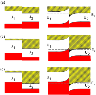
Motivated by this recent work we consider in this paper modulation doping near an interface between two-different Mott insulators, a MIMI heterojunction. The model system that we have in mind is sketched in Fig. [ 2]. Most classes of transition metal compounds are either ternary or quaternary, with additional spectator atoms that donate electrons to hybridized transition metal-oxygen orbitals near the Fermi energy. These systems can be doped by replacing the spectator atoms by atoms with a different valence. Modulation doping of a MIMI heterojuntion is achieved by doping the larger gap material at a spectator atom location that is removed from the heterojucntion. The extra electrons then enter the upper Hubbard band of the lower gap Mott insulator, creating a two-dimensional doped Mott insulator that is trapped near the heterojunction by space charge electric fields. The spatial separation between dopants and the carriers that reside in the upper or lower Hubbard bands should give rise to strongly correlated metals that are relatively free from disorder due to chemical doping, and are two-dimensional in character. These systems are illustrated schematically in Fig.[ 1]. We study these systems using both HFT and DMFT as in previous studies, and also demonstrate that a generalized Thomas-Fermi theory (TFT) can be employed to capture key qualitative physics of strongly-correlated heterostructures in a very direct way. TFT yields accurate results for charge-density profiles and for the critical doping associated with the onset of parallel conduction. We conclude that both the doping fraction and the distance between the heterojunction and the doping layer play a role in the competition that occurs between different magnetically ordered states.
In the next section we describe the single-band Hubbard model used in this paper to address modulation-doped Mott-insulator heterojunction properties. In Section III we discuss results obtained for the electronic properties of this model using HFT, TFT, and DMFT. In section IV we discuss materials which might be suitable for modulation doping of Mott insulator heterojunctions. Finally in Section V we summarize our findings and speculate on the potential of modulation doped Mott insulators.
II Single-band Hubbard Model
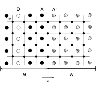
The model system we focus on this paper is sketched in Fig. 2. The heterostructure is composed of two different perovskites, and , where both and ’ are group III elements and and are group IV elements which have nominal electronic structure in this structure. Since the total number of electrons per unit cell is odd, compounds of this type must be Mott-type when they are insulators, unless translational symmetries are broken. Modulation doping is achieved by replacing some of the atoms in the larger gap insulator by elements with a different valence. In this paper we assume electron doping for convenience, although the hole doping case is completely equivalent, apart from (important!) materials specific details which we don’t attempt to model in this qualitative study. If we assume that a fraction of the atoms in a single layer of the larger gap material is replaced by donor atoms then the sum over all atom layers of the upper Hubbard band fractional occupancy must be in order to accommodate the extra electrons. When modulation doping is successful the added electrons reside in the lower gap material, placing them some distance from the ionized donor atoms and reducing the importance of the chemical disorder normally associated with doping.
For this qualitative study we use a single-band Hubbard model that ignores any orbital degeneracies that might be present. Modulation-doping depends critically on the long-range Coulomb interactions so these must be realistically represented in the model. Our model Hamiltonian includes hopping, short-range repulsion, and long-range Coulomb interaction terms , where
| (1) |
for and for . We do not account for randomness in the dopant layer in this paper. The index denotes the position of a transition metal ion () so that and respectively in a perovskite unit cell with lattice constant . For the sake of definiteness, we ignore the possibility of a d-band offset between the two materials, although these will certainly occur in practice. Given this assumption, a Type-I MIMI heterojunction will occur whenever the Hubbard parameter is large enough to produce insulating behavior in both materials. We consider a system with a finite number of layers labeled sequentially from left to right and define for to and for to with so that the larger gap material is on the left. We treat the Coulomb part of the interactions in a mean-field Hartree approximation. Since Coulomb potentials in the absence of doping are implicitly included in the model band Hamiltonian, in evaluating this potential we include only the extra charges in the dopant layer and charges due to occupancy of lower or upper Hubbard bands. To be specific, the reference background has charge per atom equal to for each site and for each , , and site. As a result, the mean-field long-ranged Coulomb interaction is:
| (2) |
where is the electron density on site .
III Type-I MIMI Heterojunction Electronic Structure
III.1 Hartree-Fock Theory
In HFT the strong on-site Coulomb interactions is also treated in a mean-field approximation so that
| (3) |
HFT is equivalent to minimizing the microscopic Hamilton in the space of Slater-determinant wavefunctions. As notedokamoto3 previously there are typically a number of self-consistent solutions of the HF equations, corresponding to a number of local minima of the Hartree-Fock energy functional. The various minima usually are distinguished by different types of magnetic order. Our philosophy in examining several different solutions without strong emphasis on their relative HF energies is that different types of order will occur near different interfaces but neither the single-band Hubbard model nor any of the electronic structure approximations we consider (or indeed any known electronic structure approximation) is sufficiently reliable to confidently select between them. Indeed phase transitions between Mott insulator states with magnetic order and paramagnetic metallic phases, corresponding to magnetic and non-magnetic extrema of the Hartree-Fock energy functional, are often first order. (We will however make some conclusions of a more qualitative nature concerning trends and tendencies related to modulation doping.) As explained more fully below, we find that the HFT electron density distribution near a MIMI heterostructure is sensitive mainly to the relative orientations of electron spins on neighbouring metal sites on adjacent layers. Consequently, we present results only for usual bipartite antiferromagnetic (AFM) and ferromagnetic (FM) states, which in this respect cover the two possibilities. These two ordered states are metastable in both undoped and modulation doped regimes for the range of parameters we have studied.
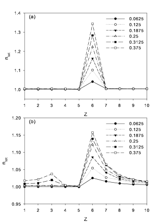
The results of our HFT calculations are summarized in Fig. 3. We have chosen typical parameters for a one-band Hubbard model of perovskite transition metal oxides, taking , , and .okamoto1 ; mizokawa We can see from Fig. 3 that the modulation doping effect occurs for both AFM and FM states, although the details of the electron density distributions are quite different in the two cases. Short-range correlations therefore appear to play a relatively strong role in determining the charge distribution near MIMI heterostructures, in contrast to the MIBI heterojunction case in which they playokamoto1 a relatively minor role. The upper Hubbard band electrons are noticeably more confined to the interface in the AFM state case and spread further into the smaller-U layer in the FM state case. This difference in density-distribution follows from a corresponding difference in the compromise between band-energy minimization and interaction energy minimization in the two-cases. The ferromagnetic state which has all spins parallel maximizes the hopping amplitudes between sites, doing a better job of minimizing band energy at a cost in interaction energy. The bandwidth of the mean-field quasiparticle states is for FM states and for AFM states. Increased doping should favor FM states over AFM states, at least within HF theory. From a real-space point of view, doping frustrates the staggered moment order of the AFM state more strongly than it frustrates the FM order because of the nearest-neighbor hopping term . In other words, doping favors the FM state over the AFM state.
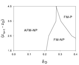
The doped electrons have a strong tendency to accumulate nearly completely in one layer in the AFM state case. Larger setback distances for the dopant layer should result in larger space-charge fields at the heterojunction and less opportunity for electrons to spread out away from the interface, robbing the ferromagnetic state of the extra stability that it gains from the third dimension. We expect therefore that for a given doping level , antiferromagnetism will be favored by a larger setback distance for the dopants. A larger setback distance also favors the development of parallel conduction channel. These trends can be seen in the ground-state phase diagram plotted in Fig. 4. In summary, modulation doping in MIMI heterostructures may make it possible not only to create weakly-disordered low-dimensional strongly correlated electron systems, but also to engineer the compromises that occur in these systems between different types of magnetic order.
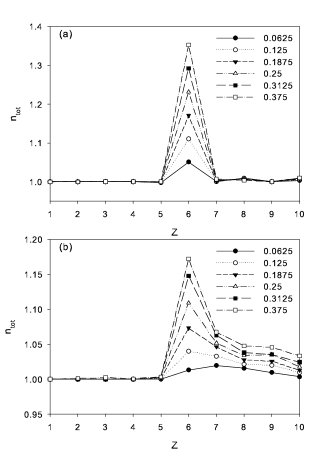
We note in Fig. 3 that for the FM state, a parallel conduction channel starts to appear adjacent to the doping layer at . For the parameters we have chosen modulation doping successfully places the carriers in a more remote layer up to this doping level.
III.2 Thomas-Fermi Theory
The HFT results can be understood using a Hubbard-model version of Thomas-Fermi theoryspruch . The TF equation for this system are:
| (4) |
where is the chemical potential at density without long-ranged Coulomb interaction and is the electrostatic potential for th layer obtained from the charge density by solving the Poisson equation. In principle, should be obtained from the exact solution of the three-dimensional Hubbard model. This input is unfortunately still unavailable. Instead, we can use HFT to obtain . In this way we have separate versions of the TF equations for AFM, FM, and PM states. As for , in the continuum limit each layer can be approximated by a 2-d uniformly-charged plane so that we have:
| (5) |
where is the layer index for of the dopant layer and is summed over all electronic layers. Fig. 5 shows results calculated using this TFT for the same parameters as used in Fig. 3. The total electron density distributions are almost identical to those obtained from the full microscopic HFT. We do note that the parallel conduction channel in the FM state appears at lower doping in TF theory than in the microscopic theory.
The local-density approximation for correlations implicit in the Thomas-Fermi theory is obviously least reliable in judging the relative chemical potentials for adding carriers to spatially separate layers. The discrepancy also occurs partly because the long-ranged Coulomb interaction was evaluated using a three-dimensional lattice version in the microscopic HFT whereas a continuum approximation for the layers was used in the TFT calculations. We expect that the TFT model is too simplified to determine the critical doping for parallel conduction accurately for any particular heterojunction, but it may be used to analyze trends.
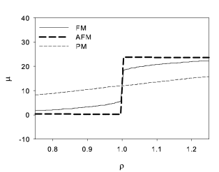
The most important consequence of strong local interactions in the Hubbard model is the emergence of a jump in the chemical potential when the electron density per site crosses from less than one to more than one. As illustrated in Fig. 6, the opening of the Hubbard gap is accompanied by slower dependence of the chemical potential on density just above and just below , i.e. by an increase in the thermodynamic density of states within the Hubbard bands. To capture these features we approximate the chemical potential in the upper Hubbard band near , by , where is the bottom of the upper Hubbard band, and is the thermodynamic density of states averaged over the energy range of interest near the bottom of the band. This notation is chosen to emphasize similarities to semiconductor heterojunction physics. Using this result in each layer we find that
| (6) |
where is the index of the first metal layer on the small U side of the heterojunction. This simple and approximate expression emphasizes that increases with , decreases with and, as in the semiconductor case, decreases with the donor layer set-back distance. ¿From HFT we estimate that for AFM states while for FM states. In both cases is approximately . As illustrated in Fig. 6, tends to be larger for AFM states than for FM states. The precise form of the thermodynamic density of states near the band edge in any particular approximation can only be determined numerically. This simple expression does not fully capture the difference between AFM and FM states, but it does capture some simple but important properties. More effective modulation doping will occur materials combinations with larger difference, and smaller (i.e. larger dielectric constant ) values. Additionally, because of stronger tendency to confine electrons in one layer in AFM state, is larger in AFM than in FM states in general. These features are confirmed by our numerical calculations.
TFT is successful because the dominating energy scales are the electrostatic energy and the correlation energy arising from local correlations. The ground state electron density distribution is a result of competition between these two energy scales, which is accurately captured by the TF approximation.
III.3 Dynamical Mean-Field Theory
HFT provides a particularly poor description of paramagnetic (PM) strongly correlated states because it is unable to capture correlated quantum fluctuations. In the limit of large it is clear that the thermodynamic properties ( for example) of a paramagnetic state are much more similar to those of ordered states than suggested by Hartree-Fock theory. To obtain a better description of paramagnetic modulation-doped electron systems we appeal to dynamical mean-field-theory DMFTgeorges1 . Full DMFT calculations are however too time consuming, even for our relatively simple model, and we therefore employ the two-site method, a minimal realization of DMFT that is able to capture the essential physics near a Mott transition.potthoff1 The two-site method has been used previously to describe a MIBI heterostructureokamoto1 . Following the general framework of DMFT and the notation used by Okamoto et al.okamoto1 , the electron Green’s function for each in-plane momentum can be written as:
| (7) |
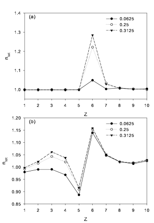
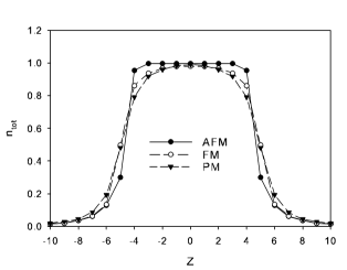
where is given in Eq. 2. The self energy is obtained by solving a two-site quantum impurity model for each layer and satisfying a set of self-consistency equationspotthoff1 ; okamoto1 . We note that the two-site method predicts that the critical value of for the metal-insulator transition of a 3-d single band Hubbard modelmp2 to be . The and values we have chosen are both larger than so that both perovskites are Mott insulators in the two-site method. Fig. 7 compares the results from DMFT and HFT for paramagnetic states. These results demonstrate that modulation doping is possible without magnetic order in DMFT. The failure of HFT in this respect is a well understood consequence of the importance of on-site correlation effects for MIMI heterostructure properties, and of the failure of HFT to capture these correlations.
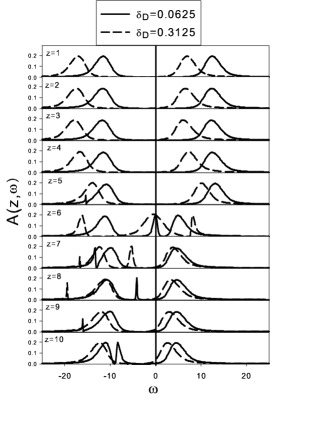
In Fig. 8 we plot DMFT layer-dependent electronic spectral functions
| (8) |
Only the layer closest to the interface on the smaller-U side ( in the figure) develops finite spectral weight near the Fermi surface upon doping. The appearance of a peak in the spectral function near the Fermi energy in layers close to the interface is reminiscent of the findings of Okamoto et al.okamoto1 for a MIBI heterojunction, who refer to this tendency as electronic surface reconstruction. The robustness of this phenomenon beyond the two-site method is not certain at present, nevertheless it is intriguing that it occurs in two quite different heterojunction systems. This finding has a natural interpretation in DMFT. In Eq. 7, acts like ”layer-resolved chemical potential,” which determines the total electron density in layer . For each layer one must solve a separate quasi two-dimensional quantum impurity model whose solution shows insulating (metallic) behavior for electron density close to (away from) 1. The self-consistency equations ensure that all solutions are related. Consequently, DMFT generally predicts that a layers with electron density away from 1 (layer 6 in the present calculation) is metallic.
III.4 Thomas-Fermi Theory for MIBI Heterostructures
Our TFT can accurately reproduce the electron density distribution near a MIBI heterostructureokamoto1 calculated in previous work. Following the notation of Okamoto and Millis, the electrostatic potential in the TF relation of Eq. 4 can be written as:
| (9) |
where . Fig. 9 shows solutions of the TF equations for AFM, FM, and PM states which are in accurate agreement with Okamoto’s results. The three-unit-cell wide crossover is clearly seen for each state. The reason for the weaker dependence on the details of on-site correlations is that many layers have electron filling smaller than one. Electrons only fill in the lower Hubbard band. As a result, the correlation gap between the Hubbard bands, which is sensitive to the details of the on-site correlation, does not affect the electronic structure very much.
IV Materials Considerations
It is still a challenge to determine model parameters appropriate for particular transition metal oxides, although a number of different approaches have been proposed. imada ; torrance ; arima ; anisimov Although not fully mutually consistent, these ideas do provide a general picture of how important model parameters vary, and are a useful rough guide to possible materials combinations that might exhibit MIMI modulation doping. materials (: Rare earth) appear to be an attractive possibility because of their relative simplicity. It has been shown that YMO3 has stronger electronic correlation than LaMO3 because of the smaller toleranceimada factor . Therefore YMO3/LaMO3 heterostructure appear to be a good candidate for realizing modulation doping. In particular LaTiO3 and YTiO3 are both Mott insulators with distorted perovskite structures (GdFeO3 type) having gaps and respectivelyokimoto . They might be used to realize a modulation doped heterostructure if YTiO3 could be doped. We emphasize that at present we do not know how the d-bands are aligned at a heterojunction between these two materials. Indeed, aside from the band-lineup issue, it is importnat to recognize that the simple model considered in this paper is not sufficiently rich to capture all aspects of the interface physics that can be relavant to modulation doping and to magnetic order in the interface layer. For example orbital degeneracy plays a key role in the magnetic state of bulk YTiO3 and in all liklihood would also play a role in determining the magnetic state of any two-dimensional matallic layer at the interface.
Although our one-band model is intended to qualitatively describe systems with cubic perovskite structure, some of our results should be generalizable. As emphasized above, the modulation doping effect is a consequence of Coulomb space-charge fields and on-site correlations. We therefore do not expect that perfect affinity to the ideal perovskite structure to be of key importance. Other type Mott insulators with =rare earth or alkaline earth and Mn,Cr might also be good candidates, although there will certainly be additional complications because of the larger -valence that are not addressed at all in this work. Building up more realistic models for potential building block materials is an important challenge for theory.
V Summary and Conclusions
In this paper, we have presented some theoretical considerations related to modulation doping near heterojunctions between two different Mott insulators, combining insights from Hartree-Fock Theory, Thomas-Fermi Theory, and Dynamical Mean-Field-Theory approaches. Using typical parameters within a simple single-band Hubbard model, we predict that modulation doping is possible with doping layers set back from the heterojunction by several lattice constants. Modulation doping can be used to create 2-d strongly correlated electron system with weak disorder and controllable densities. These systems could prove to be an interesting platform for systematic studies of strongly correlated system. Indeed, we find that the magnetic phase diagram can be altered not only by the dopant density but independently by the dopant layer setback distance. Unlike the case of MIBI heterostructures in which the Coulomb field dominates, the growth direction electron density distribution in MIMI heterojunction systems also depends strongly on the character of in-plane ordering. In the AFM state electrons are more confined to the interface while in the FM state electrons spread further away from the heterojunction into the smaller gap material. The results of HFT can be reproduced remarkably well by Thomas-Fermi theory, indicating that the electrostatic energy and the correlation energy resulting from local fluctuations dominate the physics of the heterostructure. From the TF equation, we estimate the critical doping at which modulation doping starts to fail. DMFT calculations show that modulation doping can occur without magnetic order , and that it requires only the on-site correlations that lead to the Mott-Hubbard gap. Layer-dependent spectral functions calculated using DMFT indicate that only the interface layer is metallic, reminiscent to the earlier findings of Okamoto et al.okamoto1 .
Doped Mott insulators typically appear to have exotic properties when the doping is small and more conventional properties when the doping is large and the total band filling is well away from one, the value at which local correlations have maximum importance. In the case of the extremely heavily studied cuprate systems, for example, this crossover is interrupted, by high-temperature superconductivity. It is interesting to consider whether or not the two-dimensional electron systems considered in this paper are Fermi liquids. Whereas bulk doping often leads eventually to a first order transitions between a doped Mott insulator and a relatively conventional metal, modulation doping in a single or several layers may make it possible to realize high-density, low-disorder, two-dimensional exotic metals which carry reflect the heritage of the three-dimensional Mott insulators from which they emerge. Since the very existence of these two-dimensional electronic systems depends on gaps that are entirely due to electron-electron interactions, it is clear that they cannot be adiabatically connected to non-interacting electron states. On the other hand, in the HFT description the doped state is a Fermi liquid with well defined quasiparticles. This approximation neglects quantum fluctuations of the magnetic state however, and its predictions for quasiparticle properties may not be reliable.
We have also speculated briefly on materials combinations that might be attractive to realize the physics discussed in this paper. Predictions of the phase diagram for particular materials combinations will require much more detailed modeling, and may be assisted by insights from experiment as well as from ab initio electronic structureNoguera2004 ; Sawatzky calculations. A detailed description would require many realistic features of perovskite materials to be addressed, for instance lattice distortionsgoodenough ; sawatzkypreprint which may vary with proximity to the interface, and related orbital degeneracy issues. Progress will require progress in materials growth and characterization and interplay with ab initio and phenomenological modelling.
VI Acknowledgments
This work was supported by the Welch Foundation. The authors acknowledge helpful discussions with Bernhard Keimer, Karin Rabe, George Sawatzky, David Singh, and John Goodenough. W.-C. Lee would like to thank Satoshi Okamoto for sharing precious experiences in DMFT.
References
- (1) M. Imada, A. Fujimori, and Y. Tokura, Rev. Mod. Phys. 70, 1039 (1998).
- (2) Y. Tokura and N. Nagaosa, Science 288, 462 (2000).
- (3) E. Dagotto, Science 309, 257 (2005).
- (4) C. H. Ahn, S. Gariglio, P. Paruch, T. Tybell, L. Antognazza, and J.-M. Triscone, Science 284, 1152 (1999).
- (5) For an overview, see C. H. Ahn, J.-M. Triscone, and J. Mannhart, Nature 424, 1015 (2003).
- (6) A. Ohtomo, D.A. Muller, J.L. Grazul, and H.Y. Hwang, Nature 419, 378 (2002).
- (7) J. Chakhalian, J.W. Freeland, G. Srajer, J. Strempfer, G. Khaliullin, J.C. Cezar, T. Charlton, R. Dalgliesh, C. Bernhard, G. Cristiani, H-U. Habermeier and B. Keimer, Nature Physics 2, 244 (2006).
- (8) M. Potthoff and W. Notling, Phys. Rev. B 60, 7834 (1999).
- (9) R. Matzdorf, Z. Fang, Ismail, Jiandi Zhang, T. Kimura, Y. Tokura, K. Terakura, and E.W. Plummer, Science 289, 746 (2000).
- (10) Z. Fang, I. V. Solovyev, and K. Terakura, Phys. Rev. Lett. 84, 3169 (2000).
- (11) S. Schwieger, M. Potthoff, and W. Nolting, Phys. Rev. B 67, 165408 (2003).
- (12) A. Liebsch, Phys. Rev. Lett. 90, 096401 (2003).
- (13) M. Dawber, C. Lichtensteiger, M. Cantoni, M. Veithen, P. Ghosez, K. Johnston, K.M. Rabe, and J.-M. Triscone, Phys. Rev. Lett. 95, 177601 (2005).
- (14) B.K. Nikolic, J.K. Freericks, and P. Miller, Phys. Rev. B 65, 064529 (2002); J.K. Freericks, Phys. Rev. B 70 195342 (2004).
- (15) S. Okamoto and A.J. Millis, Phys. Rev. B 70, 241104(R) (2004).
- (16) S. Okamoto and A.J. Millis, Nature 428, 630 (2004).
- (17) S. Okamoto and A.J. Millis, Phys. Rev. B 70, 075101 (2004).
- (18) R. Hesper, L. H. Tjeng, A. Heeres, and G. A. Sawatzky, Phys. Rev. B 62, 16046 (2000).
- (19) C. Noguara, J. Phys. Condens. Matter. 12, R367 (2000).
- (20) T. Mizokawa and A. Fujimori, Phys. Rev. B 51, 12880 (1995)
- (21) For a review, see L. Spruch, Rev. Mod. Phys. 63, 151 (1991)
- (22) A. Georges, G. Kotliar, W. Krauth, and M. J. Rozenberg, Rev. Mod. Phys. 68 13 (1996).
- (23) M. Potthoff, Phys. Rev. B 64, 165114 (2001)
- (24) J.B. Torrance, P. Lacore, C. Asavaroengchai, and R. M. Metzger, Physica C 182, 351 (1991).
- (25) T. Arima, Y. Tokura, and J.B. Torrance, Phys. Rev. B 48, 17006 (1993).
- (26) V.I. Anisimov, J. Zaanen, and O.K. Andersen, Phys. Rev. B 44, 943 (1992).
- (27) Y. Okimoto, T. Katsufuji, Y. Okada, T. Arima, and Y. Tokura, Phys. Rev. B 51, 9581 (1995).
- (28) C. Noguera, F. Finocchi and J. Goniakowski, J. Phys. Condens. Matt. 16, 2509 (2004).
- (29) N. Pavlenko, I. Elfimov, T. Kopp, and G.A. Sawatzky, cond-mat/0605589.
- (30) see, for example, J.B. Goodenough, Structure and Bonding, Volume 98, p1-16, (Feb 2001).