Single-mode heat conduction by photons
††preprint:Electrical conductance is quantized in units of in ballistic one-dimensional conductors wees88 ; wharam88 . Similarly, thermal conductance at temperature is expected to be limited by the quantum of thermal conductance of one mode, , when physical dimensions are small in comparison to characteristic wavelength of the carriers pendry83 . The relation between and obeys the Wiedemann-Franz law ashcroft76 for ballistic electrons (apart from factor 2 in due to spin degeneracy) greiner97 , but somewhat amazingly the same expression of is expected to hold also for phonons and photons, or any other particles with arbitrary exclusion statistics rego99 ; blencowe00 . The single-mode heat conductance is particularly relevant in nano-structures, e.g., when studying heat conduction by phonons in dielectric materials schwab00 , or cooling of electrons in metals at very low temperatures schmidt04 . Here we show, based on our experimental results, that at low temperatures heat is transferred by photon radiation, in our case along a superconducting line, when electron-phonon roukes85 as well as normal electronic heat conduction are frozen out. Thermal conductance is limited by , approaching this value towards low temperatures. Our observation has implications on, e.g., performance and design of ultra-sensitive bolometers and electronic micro-refrigerators giazotto06 , whose operation is largely dependent on weak thermal coupling between the device and its environment.
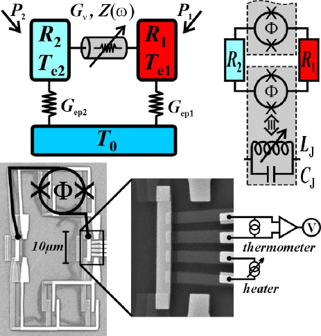
To get a picture of the radiative thermal coupling, we start by considering two resistors at temperatures and , whose resistances are and , respectively, connected via a frequency () dependent impedance , see Fig. 1. For simplicity we assume to be fully reactive, so that only the two resistors emit and absorb noise heating. The net power flow between the two resistors from 1 to 2 due to the electron-photon coupling is then given by pendry83 ; schmidt04
| (1) |
Here, is the total series impedance of the circuit, and are the boson occupation factors at the temperatures of the resistors . Specifically, for a lossless direct connection of the two resistors, , we can integrate (1) easily with the result
| (2) |
Here is the matching factor, which obtains its maximum value of unity, when . Thermal conductance by the photonic coupling, , defined as the linear response of for small temperature difference around can then be obtained from (2) for the lossless connection as
| (3) |
Thus it attains the maximum value for a single transmission channel, the quantum of thermal conductance, in a matched circuit. This result is predicted to hold not only for such photon-mediated coupling, but much more generally for carriers of arbitrary exclusion statistics wilczek82 ; haldane91 from bosons to fermions rego99 ; kane96 ; kane97 .
Due to its relatively weak temperature dependence, , electron-photon coupling is expected to become the dominant relaxation means at sufficiently low . The competing electron-phonon thermal conductance behaves normally as , where is a material parameter and is the volume of the resistor. This result derives from the expression of heat flux from electrons to lattice, , where and are the temperatures of the electrons in the resistor and of the lattice, respectively roukes85 . Equating from (3) and , one finds the cross-over temperature, , below which the photonic conductance should dominate: schmidt04 . For typical metals, for which Wm-3K-5, for mesoscopic resistors with m3, and for matching where is not too low as compared to unity, one obtains mK. Such temperatures are in the range of experiments that we describe here. By state-of-the-art electron-beam lithography one can obtain metallic islands of volumes as small as m3 pashkin00 , and there could be as high as several K.
To investigate the electron-photon thermal conduction experimentally we have imbedded a tunable impedance between the two resistors. This allows us to measure the modulation of , or , in response to the externally controllable impedance . In practice the two resistors are connected to each other symmetrically by two aluminium superconducting lines, interrupted by a DC-SQUID (Superconducting Quantum Interference Device) in each line, as shown in the electron micrograph and in the electrical model in Fig. 1. These SQUIDs serve as the thermal switches between the resistors as will be described below.
The structures have been fabricated by electron-beam lithography and three angle shadow evaporation. The film thickness of the superconducting lines is 20 nm. The two AuPd resistors are nominally identical, 6.6 m long, 0.8 m wide and 15 nm thick. Their resistances are each. One of them, say , is connected by four NIS (normal-insulator-superconductor) tunnel junctions to external aluminium leads to allow for thermometry nahum93 and Joule heating. The normal state resistance of each NIS junction is about 50 k. The resistors are connected by direct NS contacts to the superconducting lines in between, without a tunnel barrier. The resistors are, however, long enough such that they are not affected by proximity superconductivity noticeably. This is verified by the measured tunnel characteristics of the nearby NIS tunnel junctions. Due to the superconductors at a low working temperature, which is typically a factor of ten below the critical temperature K of aluminium, the normal electronic thermal conductance along the lines is efficiently suppressed.
Each DC-SQUID can be modelled as a parallel connection of a Josephson inductance and capacitance . can be tuned by external magnetic flux threading through the DC-SQUID loop, since the critical current is . Here is the Ambegaokar-Baratoff critical current ambegaokar63 determined by geometry and materials, and Wb is the flux quantum. Capacitance is a constant determined by geometry and materials.
The length of the lines connecting resistors and is m, i.e., much shorter than the typical thermal wavelength , which is several centimetres at 100 mK; here m/s is the speed of light on silicon substrate. Therefore we do not need to consider a distributed electrical model with a transmission line, but instead is effectively a lumped series connection of two circuits, i.e., . Here and we have assumed for simplicity that the two DC-SQUIDs are identical and they are exposed to the same magnetic field. This is expected to be a good approximation in view of the symmetric experimental configuration. The net heat flow between 1 and 2 is then given by
| (4) |
where the matching parameters now depend on temperature as
| (5) |
Above we have defined and .
For the full description, we still need a thermal model incorporating the two competing relaxation mechanisms, due photons and phonons, respectively. This is schematically depicted in Fig. 1, where the temperature in each resistor tends to relax via electron-phonon coupling to the constant temperature of the bath, and towards a common temperature of the two resistors via the tunable photonic conductance . denotes the external heat leak into resistor : due to wire connections has a significant non-zero value even in the absence of intentional heating, whereas turns out to be very small, since the corresponding resistor is not connected directly to external leads. We may describe the steady state of the system by thermal master equations
| (6) |
where equals for , and for , and is the volume of resistor . Equations (6) combined with (5) can be solved numerically to obtain the temperatures under given conditions.
The experiments were performed in a 3He-4He dilution refrigerator at temperatures from 30 mK up to several hundred mK. All the measurement wiring was carefully filtered and essentially only DC signals were employed. A typical measurement was done as follows. One of the SINIS tunnel junction pairs connected to resistor 1 was used as a thermometer by applying a small ( pA) DC current through it and by measuring the corresponding temperature dependent voltage. When biased at a low enough current, high sensitivity is obtained without significant self-heating or self-cooling effects giazotto06 . The SINIS thermometer is then calibrated by measuring this voltage against the bath temperature , by slowly sweeping the temperature of the mixing chamber through the range of interest, from about 40 mK up to about 300 mK. The actual measurements of thermal coupling are then done by stabilizing the bath at a desired temperature. Then we apply slow sweeps (/min) of external magnetic flux, which threads the two DC-SQUID loops nominally identically. A typical amplitude of the field sweep is such that it corresponds to 4 - 5 flux quanta through each DC-SQUID. In our geometry this corresponds to a field of about 100 T. SINIS thermometer reading is then averaged over several tens of such field sweeps, to measure accurately the periodic variation of in response to the field sweep.
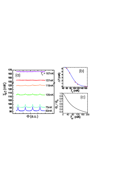
Figure 2 shows results of a measurement at a few bath temperatures as described above. We see that the modulation of in response to magnetic flux is about 6 mK at the lowest bath temperature and it decreases monotonically when is increased. Based on this data and our electrical and thermal models above, we expect that the maxima in correspond to the weakest electron-photon coupling at half-integer values of . In Fig. 2 (b) we plot with circles the corresponding modulation amplitude of between its maximum and minimum values, , as a function of for the experimental data in (a). We have added to the figure a solid line from our theoretical model assuming , fW, , nA. The last value is a fit parameter, since we cannot measure it directly in our geometry, but it is in line with the measured values of critical currents of DC-SQUIDs that we fabricated with the same parameters separately. We set fF based on the geometry of the device. Additionally, we use a typical value WK-5m-3 giazotto06 , and m3 for both resistors. The latter corresponds to the volume of each resistor excluding the overlap areas of NS contacts. The agreement between the experiment and the model is very good and we therefore use these very realistic parameters in analyzing all the results in this article. These data imply, see Fig. 2 (c), that at integer values of lies in the range 0.6…0.3, when we vary temperature from mK (the approximate value of at the minimum bath temperature) up to 200 mK, i.e., the electron-photon conductance is about one half of its quantum value in our experiment. Note that approaches the quantum of thermal conductance upon lowering temperature, since the thermal frequency decreases linearly with , and the line impedance at low frequencies, determined by , decreases likewise.
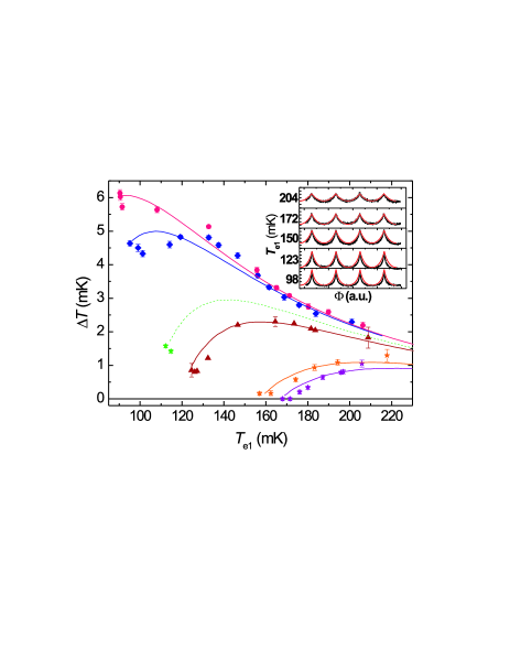
Next we present experiments where external power was applied to resistor 1, using the second pair of tunnel junctions connected to it as a heater. Figure 3 demonstrates such measurements at different bath temperatures. Compared to the data at the lowest bath temperature of 60 mK where essentially monotonic decrease of can be observed, the intermediate bath temperature data demonstrates non-monotonic dependence with initial increase of the signal on increasing the heating, and then slow decrease towards higher power levels and . Finally, at the highest values of , the signal is first absent but emerges upon increasing the input power. This behaviour arises because by applying Joule heating to just one resistor, we can establish a larger temperature difference between the two. Yet at large enough levels of , the overall temperature of the system increases, and the significance of the photon coupling with respect to electron-phonon coupling is diminishing, and the temperature modulation becomes very weak. All these dependences are fully consistent with our theoretical modelling of the system, and we obtain quantitative agreement with the data by using the same electrical and thermal parameters of the system as when modelling data of Fig. 2. The theoretical lines in Fig. 3 are the result of this modelling. In the inset of Fig. 3 we show a few full modulation curves of vs. at the bath temperature of 75 mK. The black lines are from experiment and the red ones from the theoretical model. The theoretical lines catch the main features of the shape of the experimental curves.
Prior to our experiment, the electron system like the one discussed in this article was assumed to be efficiently decoupled from the environment once the electron-phonon coupling is suppressed at low temperatures. Therefore, the observed photonic conductance has implications on performance and design of micro-bolometers and calorimeters, where efficient suppression of thermal coupling is usually taken for granted. Due to better coupling to the environment by photon conductance, the expected sensitivity of such devices is reduced, and their noise is enhanced. On the other hand, this mechanism could possibly provide a way to tune the thermal coupling of a bolometer to the heat bath in order to optimize its operation, which is a trade-off between sensitivity and bandwidth. The radiation of heat can possibly be benefitted also in removing excessive heat, e.g., on dissipative shunt resistors of ultra-sensitive or very low temperature SQUIDs savin06 , or at the back side of an electronic micro-refrigerator clark04 . Furthermore, the photonic coupling could act as a mediator of decoherence, e.g., on solid-state quantum coherent devices schon01 . The strength of this harmful effect depends, like in our present experiment, critically on matching between the noise source and the system that it affects on.
References
- (1) van Wees, B.J. et al., Quantized conductance of point contacts in a two-dimensional electron-gas, Phys. Rev. Lett. 60, 848-850 (1988).
- (2) Wharam, D.A. et al., One-dimensional transport and the quantisation of the ballistic resistance, J. Phys. C 21, L209-L214 (1988).
- (3) Pendry, J.B., Quantum limits to flow of information and entropy, J. Phys. A 16, 2161-2171 (1983).
- (4) See, e.g., Ashcroft, N.W. and Mermin N.D., Solid State Physics (Holt, Rinehart and Winston, New York, 1976).
- (5) Greiner, A., Reggiani, L., Kuhn, T., and Varani, L., Thermal Conductivity and Lorenz Number for One-Dimensional Ballistic Transport, Phys. Rev. Lett. 78, 1114-1117 (1997).
- (6) Rego, L.G.C. and Kirczenow, G., Fractional exclusion statistics and the universal quantum of thermal conductance: A unifying approach, Phys. Rev. B 59, 13080-13086 (1999).
- (7) Blencowe, M.P. and Vitelli, V., Universal quantum limits on single-channel information, entropy, and heat flow, Phys. Rev. B 62, 052104 (2000).
- (8) Schwab, K., Henriksen, E.A., Worlock, J.M., and Roukes, M.L., Measurement of the quantum of thermal conductance, Nature 404, 974-977 (2000).
- (9) Schmidt, D.R., Schoelkopf, R.J., and Cleland, A.N., Photon-mediated thermal relaxation of electrons in nanostructures, Phys. Rev. Lett. 93, 045901 (2004).
- (10) Roukes, M.L., Freeman, M.R., Germain, R.S., Richardson, R.C., and Ketchen, M.B., Hot electrons and energy transport in metals at millikelvin temperatures, Phys. Rev. Lett. 55, 422-425 (1985).
- (11) Giazotto, F., Heikkilä, T.T., Luukanen, A., Savin, A.M., and Pekola, J.P., Opportunities for mesoscopics in thermometry and refrigeration: Physics and applications, Rev. Mod. Phys. 78, 217-274 (2006).
- (12) Wilczek, F., Quantum mechanics of fractional-spin particles, Phys. Rev. Lett. 49, 957-959 (1982).
- (13) Haldane, F.D.M., “Fractional statistics” in arbitrary dimensions: A generalization of the Pauli principle, Phys. Rev. Lett. 67, 937-940 (1991).
- (14) Kane, C.L. and Fisher, M.P.A., Thermal Transport in a Luttinger Liquid, Phys. Rev. Lett. 76, 3192-3195 (1996).
- (15) Kane, C.L. and Fisher, M.P.A., Quantized thermal transport in the fractional quantum Hall effect , Phys. Rev. B 55, 15832-15837 (1997).
- (16) Pashkin, Yu.A,, Nakamura, Y, and Tsai, J.S., Room-temperature Al single-electron transistor made by electron-beam lithography, Appl. Phys. Lett. 76, 2256-2258 (2000).
- (17) Nahum, M. and Martinis, J.M., Ultrasensitive-hot-electron microbolometer, Appl. Phys. Lett. 63, 3075-3077 (1993).
- (18) Ambegaokar, V. and Baratoff, A., Tunneling between superconductors, Phys. Rev. Lett. 10, 486-489 (1963).
- (19) Savin, A.M., Pekola, J.P., Averin, D.V., and Semenov, V.K., Thermal budget of superconducting digital circuits at subkelvin temperatures, J. Appl. Phys. 99, 084501 (2006).
- (20) Clark, A.M., Williams, A., Ruggiero, S.T., van den Berg, M.L., and Ullom, J.N., Practical electron-tunneling refrigerator, Appl. Phys. Lett. 84, 625-627 (2004).
- (21) Makhlin, Yu., Schön, G., and Shnirman, A., Quantum-state engineering with Josephson-junction devices, Rev. Mod. Phys. 73, 357-400 (2001).
Acknowledgements We thank Mikko Paalanen, Dmitri Averin, Arttu Luukanen, Hugues Pothier, Frank Hekking and Gerd Schön for useful comments, and Academy of Finland (TULE) and the EC-funded ULTI Project, Transnational Access in Programme FP6 (Contract #RITA-CT-2003-505313) for financial support.