- Josephson tunnel junctions with ferromagnetic barrier
Abstract
We fabricated high quality Nb/Al2O3/Ni0.6Cu0.4/Nb superconductor-insulator-ferromagnet-superconductor Josephson tunnel junctions. Using a ferromagnetic layer with a step-like thickness, we obtain a - junction, with equal lengths and critical currents of 0 and parts. The ground state of our () long junction corresponds to a spontaneous vortex of supercurrent pinned at the 0- step and carrying of the magnetic flux quantum . The dependence of the critical current on the applied magnetic field shows a clear minimum in the vicinity of zero field.
pacs:
74.50.+r,85.25.Cp 74.78.Fk 74.81.-gIn his classical paperJosephson (1962) Brian Josephson predicted that the supercurrent through a Josephson junction (JJ) is given by . Here, is the Josephson phase (the difference of phases of the quantum mechanical wave functions describing the superconducting condensate in the electrodes), and is the critical current (maximum supercurrent that one can pass through the JJ). When one passes no current (), the Josephson phase corresponds to the minimum of energy (ground state). The solution corresponds to the energy maximum and is unstable. Later it was suggested that using a ferromagnetic barrier one can realize JJs where Bulaevskiĭ et al. (1977). Such junctions obviously have in the ground state and, therefore, are called JJs. The solution corresponds to the energy maximum and is unstable.
JJs were recently realized using superconductor-ferromagnet-superconductor (SFS)Ryazanov et al. (2001); Sellier et al. (2004); Blum et al. (2002); Bauer et al. (2004), superconductor-insulator-ferromagnet-superconductor (SIFS)Kontos et al. (2002) and otherBaselmans et al. (1999) technologies. In these junctions the sign of the critical current and, therefore, the phase (0 or ) in the ground state, depends on the thickness of the ferromagnetic layer and on temperature Buzdin (2005). JJs may substantially improve parameters of various classical and quantum electronic circuitsTerzioglu and Beasley (1998); Ustinov and Kaplunenko (2003); Ortlepp et al. (2006); Ioffe et al. (1999); Yamashita et al. (2005); Yamashita et al. (2006). To use JJs not only as a “phase battery”, but also as an active (switching) element in various circuits it is important to have a rather high characteristic voltage (defined e.g. as at ) and low damping. For example, for classical single flux quantum logic circuits defines the speed of operation. For qubits the value of a quasi-particle resistance at should be high enough since it defines the decoherence time of the circuits. Both high values of and can be achieved by using tunnel SIFS JJs rather than SFS JJs.
The dissipation in SIFS JJs decreases exponentially at low temperaturesWeides et al. , thus, making SIFS technology an appropriate candidate for creating low decoherence quantum circuits, e.g., qubits.Ioffe et al. (1999); Yamashita et al. (2005); Yamashita et al. (2006).
Actually, the most interesting situation is when one half of the JJ () behaves as a 0 JJ, and the other half () as a JJ (a 0- JJ)Bulaevskii et al. (1978): In the symmetric case (equal critical currents and lengths of and parts) the ground state of such a 0- JJ corresponds to a spontaneously formed vortex of supercurrent circulating around the 0- boundary, generating magnetic flux inside the junctionBulaevskii et al. (1978). In a very long JJ with length (Josephson penetration depth) the vortex has the size and carries the flux — the so-called semifluxonXu et al. (1995); Goldobin et al. (2002). Semifluxons are actively studied during the last yearsKirtley et al. (1997); Stefanakis (2002); Goldobin et al. (2003); Zenchuk and Goldobin (2004); Goldobin et al. (2004a); Susanto et al. (2003); Goldobin et al. (2004b); Lazarides (2004); Kato and Imada (1997); Koyama et al. (2005); Goldobin et al. (2005). For the vortex does not “fit” into the junction and the flux inside the junction Kirtley et al. (1997). In any case the ground state is degenerate, i.e. may have positive or negative spontaneously formed fractional flux (clockwise or counterclockwise circulating supercurrent) and can be considered as two states (up and down) of a macroscopic spin.
Before, 0- JJs were realized using d-wave superconductorsVan Harlingen (1995); Tsuei and Kirtley (2000); Chesca et al. (2002); Smilde et al. (2002); Ariando et al. (2005), the semifluxons spontaneously formed at the 0- boundary were observedKirtley et al. (1999); Sugimoto et al. (2002); Hilgenkamp et al. (2003); Kirtley et al. (2005), and with a minimum at an external magnetic field was measuredVan Harlingen (1995); Smilde et al. (2002); Ariando et al. (2005). However, the phase shift of in such structures takes place not inside the barrier, but inside the d-wave superconductor. 0- JJs were also obtained (by chance) using SFS technologyDella Rocca et al. (2005); Frolov et al. (2006), but such structures are quite difficult to measure because of the extremely small . In Ref. Della Rocca et al., 2005 the presence of spontaneous fractional flux was detected by an auxiliary SIS JJ coupled with the 0- SFS JJ. In Ref. Frolov et al., 2006 the was measured using a SQUID-voltmeter.
In this letter we present the first intentionally made symmetric 0- tunnel JJ of SIFS type with large , making direct transport measurements of feasible. Our JJ has a ground state with macroscopic current circulating around the long structure. Such 0, and 0- JJs open a road to self-biased classical and quantum electronic circuits. Moreover, one can study the physics of semifluxons in 0- JJs and, especially, their quantum behavior.
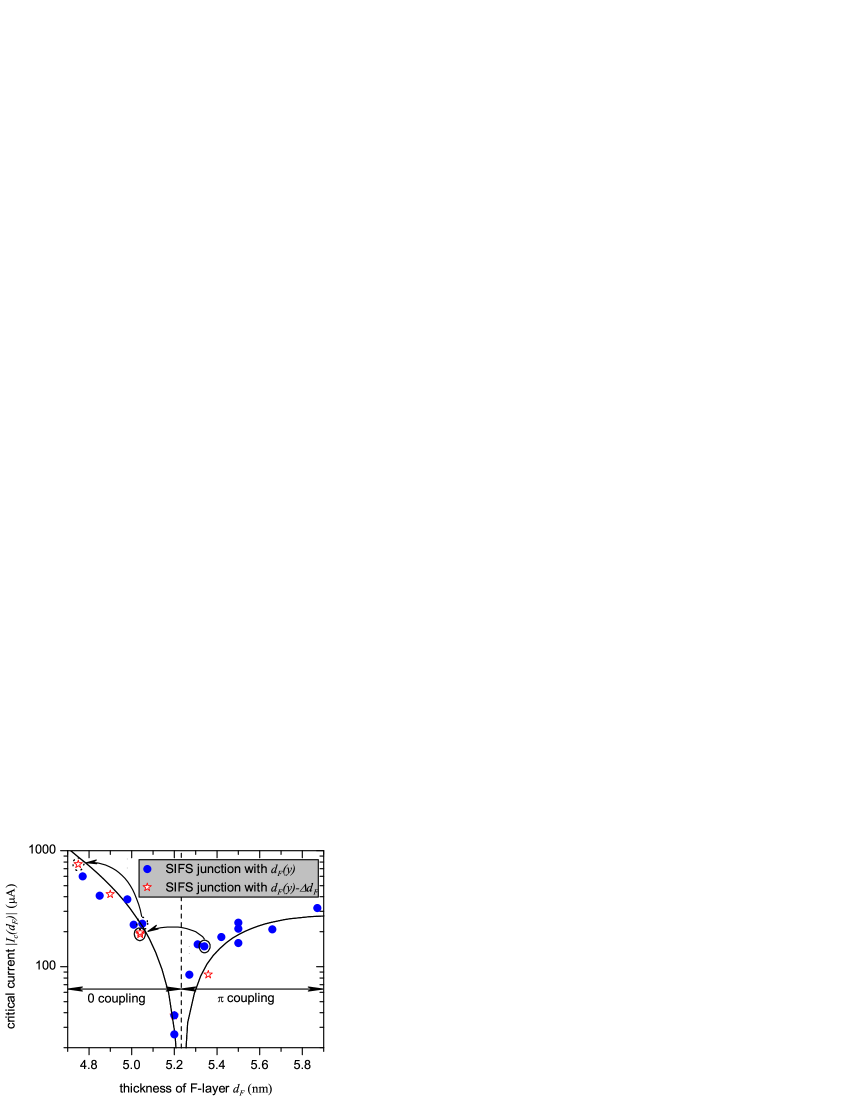
The idea of SIFS based 0- JJs is the following. It is knownBuzdin (2005) that the critical current of SIFS JJs changes its sign (and the ground state from to ) as a function of the F-layer thickness , as shown in Fig. 1 by the continuous line (c.f. Fig. 2 of Ref. Kontos et al., 2002 or Fig. 1 of Ref. Weides et al., ). By choosing two F-layer thicknesses (e.g. , ) such that , we fabricate a SIFS structure with a step-like to obtain a 0- JJ sketched inside Fig. 4.
The SIFS junctions were fabricated using a heterostructure. All 0, and 0- JJs were fabricated within the same technological process. First, Nb-Al2O3 bottom layers were fabricated as for usual high SIS JJsWeides et al. (2006, ). Second, we have sputtered an F-layer with a gradient of thicknessWeides et al. (2006); Vohl et al. (1991); Kim et al. (2005); Zdravkov et al. (2006) in direction. Various structures on the chip where placed within a narrow ribbon along direction. Such ribbons were replicated along -direction, so that we have the same set of structures for different along the axis from down to over the 4 in. wafer. After the deposition of a Nb cap-layer and lift-off we obtain the complete SIFS stack with F-layer thickness , but without steps in yet. To produce steps, the (parts of) JJs that are supposed to have larger are protected by photo resist. Then the Nb cap-layer is removed by SF6 reactive rf etching, which leaves a homogeneous flat NiCu surface. About () of NiCu were further Ar ion etched. The above two-step etching and subsequent deposition of a new Nb cap-layer were done in-situ. Subsequently the junctions were patterned by a three level photolithographic procedure Gurvitch et al. (1983) and insulated by formed by anodic oxidation after ion-beam etching down to the bottom -electrode.
Each set of JJs (along one ribbon) has JJs of three classes: (a) not affected by etching with F-layer thickness , (b) etched uniformly with F-layer thickness , and (c) etched to have a step-like . All junctions had an area of and lateral sizes comparable to or smaller than .
We have measured the critical currents of class (a) JJs (filled blue circles) and class (b) JJs (open red stars) with dimensions (Fig. 1).
For low-transparency SIFS junctions is given by
| (1) |
where are the decay and oscillation lengthsWeides et al. . The coupling changes from to at the crossover thickness . Fitting of the non-etched junctions (class a) using Eq. (1), we estimate and and , i.e., Weides et al. . The curve given by Eq. (1) with such values of and is shown in Fig. 1 by a continuous line. Comparing it with the experimental data for the etched samples (class b) we estimate the etched-away F-layer thickness as . The open red stars in Fig. 1 are shown already shifted by this amount.
Now we choose the set of junctions ( of the ribbon) which before etching have thickness and critical current ( junction) and after etching have thickness and critical current (0 junction). One of the possibilities is to choose the junction set denoted by closed circles around the data points in Fig. 1, i.e. and .
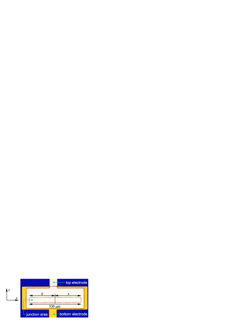
Further we deal only with three JJs out of the selected set: (1) a reference SIFS 0 JJ with F-layer thickness and critical current density ; (2) a reference SIFS JJ with F-layer thickness and critical current density ; and (3) a SIFS 0- JJ with thicknesses , and critical current densities , in the 0 and halves, respectively. All these junctions have dimensions (, ). The 0- JJ (see Fig. 2) consists of one 0 and one region of equal lengths (within lithographic accuracy).
For all three junctions we have measured the – characteristics (IVCs) and with applied in direction. At the IVCs have no hysteresis and the critical currents of the reference 0 and JJs were , , respectively. The dependences and are almost perfect Fraunhofer patterns, shown in Fig. 3(a). For the 0- JJ, is somewhat asymmetric (e.g. near the first minimum) because of , but has a clear minimum near zero field. To achieve more symmetric configuration we have measured for all three JJs in a temperature range down to , because decreasing temperature should increase faster than . Two effects are responsible for this behavior. First, when decreases, the 0- crossover thickness decreases, decreasing and increasing . Second, the whole amplitude of grows as the temperature decreases, similar to the Ambegaokar-Bartoff dependence for conventional SIS JJ. For these two dependences have opposite effect, while for they add up. Thus, as decreases, increases faster than .
While cooling down and making measurements at each , one of the JJs (, or –) after h was eventually trapping some flux that we associate with rearrangement of the domains in the F-layer — was suddenly shifting along the -axis. After thermal cycling, the same symmetric could be measured again.
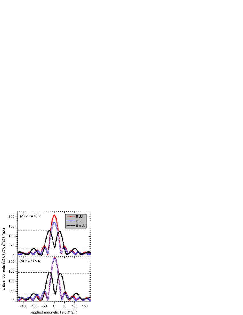
The main experimental result of the paper is presented in Fig. 3(b), which shows for all three junctions at . At this temperature and almost coincide, yielding Fraunhofer patterns with critical currents , and the same period of modulation. has a clear minimum near zero field and almost no asymmetry — the critical currents at the left and right maxima ( and ) differ by less than .
To ensure that the dip on near zero field originates from - we also measured by applying a field along direction. In this case the pattern looks like a Fraunhofer pattern with maximum at zero field (not shown).
Let us discuss the features of this dependence and its meaning. The Josephson penetration depth is estimated by taking the London penetration depth , the thicknesses of the superconducting electrodes and , and . Thus, the normalized length of our JJs is at .
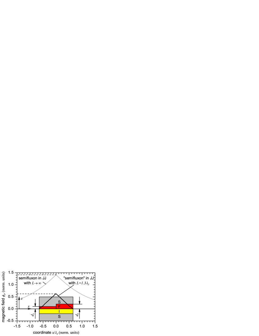
What is the ground state () of our 0- JJ? For the symmetric 0- LJJ of length the ground state has a spontaneous fluxKirtley et al. (1997) , i.e. of . If the 0- JJ is asymmetric, e.g., , the ground state may correspond to or . In our case, using formulas from Ref. Bulaevskii et al., 1978 and our value of , we estimate that the ground state with spontaneous flux exists at from to . Thus we are clearly inside the domain with spontaneous flux in the ground state for , although one cannot see any striking indications of spontaneous flux on . Note, that for shorter JJs () the range of with spontaneous flux in the ground state may be extremely small. We would like to point out that even if is off this domain, e.g., at higher when the asymmetry is even larger, and the ground state is flat ( in this case), by applying a bias current (even at ) or magnetic field one immediately induces fractional flux in the system.Goldobin et al. (2003) The magnetic field corresponding to our “semifluxon” at is shown in Fig. 4
Using a short JJ model, i.e. assuming that the phase is a linear function of , we can calculate that the first minimum of the Fraunhofer dependence for a 0 or for a JJ should be at , where the effective magnetic thickness of the junction . As we see the experimental value of is lower by a factor of due to field focusing. In a short JJ model, should look likeVan Harlingen (1995)
| (2) |
where is the applied number of flux quanta through the effective junction area (). This dependence has , two symmetric maxima at and the first side minima at , which should have a parabolic shape touching the axis. We have some discrepancies between the simple short junction theory (2) and experiment (Fig. 3).
First, in our experiment the minimum of is somewhat lifted from zero up to . Second, the critical current at the side maxima , are below the theoretical value of 0.72 and are a little bit different. Third, the first side minima of are reached at the same as the second minima of for the 0 or JJs, which is good, but the minima look oblate-shaped from the bottom and do not reach zero.
All these effects can be explained and reproduced numerically by taking into account several additional ingredients. First, the value of at the central minimum is affected by the finite length of the junction, i.e. the deviation from the short JJ model increases at the central minimum. Second, if we include in the short JJ model, instead of curve (2), we will get a symmetric curve with , and maximum below 0.72. This explains why in Fig. 3(a) the value of at the minimum is larger than in Fig. 3(b). If, instead we assume some weak net magnetization of the F-layer, such that (in the 0 part) is not equal to (in the part), we find that shifts along the axis by , as seen in Fig. 3. If we include both assumptions, will also get asymmetric maxima and the characteristic oblate-shape at the first side minima. Details will be presented elsewhere.
In summary, we have fabricated high quality superconductor-insulator-ferromagnet-superconductor Josephson tunnel junctions. Using a ferromagnetic layer with a step-like thickness, we obtained a - junction, which becomes symmetric at and carries spontaneous fractional flux in the ground state. The dependence of critical current on the applied magnetic field shows a clear minimum in the vicinity of zero field and is well described by Eq. (2). In essence our data are the same as for 0- JJs based of d-wave superconductors such as corner JJsVan Harlingen (1995), bi-, tri- and tetra- crystal JJsTsuei and Kirtley (2000); Chesca et al. (2002), and YBCO-Nb or NCCO-Nb ramp zigzag JJsSmilde et al. (2002); Ariando et al. (2005). This is not suprising since the underlaying modelXu et al. (1995); Kirtley et al. (1997); Goldobin et al. (2002) is the same. To our knowledge our SIFS 0- JJ is the first underdamped tunnel 0- junction based on low- superconductors. It can be measured using standard setups due to the rather high characteristic voltage . The possibility to fabricate 0, and 0- Josephson junctions within the same process, having the same and opens perspectives for application of SIFS technology in complimentary logic circuitsTerzioglu and Beasley (1998), in RSFQ with active junctionsOrtlepp et al. (2006), in qubits Ioffe et al. (1999); Yamashita et al. (2005); Yamashita et al. (2006) as well as for the investigation of semifluxons. Due to exponentially decreasing damping for Weides et al. (c.f. in d-wave based 0- JJs damping is larger and does not decrease exponentially), SIFS 0- JJs are promising devices for observation of macroscopic quantum effects using semifluxons (macroscopic spins) and for qubitsKato and Imada (1997); Goldobin et al. (2005).
We thank A. Buzdin, V. Oboznov and V. Ryzanov for useful discussions. This work is supported by the ESF program PiShift and by the Deutsche Forschungsgemeinschaft projects GO-1106/1, KL-930/10 and SFB/TR 21. E.G. acknowledges support by the Eliteförderprogram of the Landesstiftung Baden-Württemberg.
References
- Josephson (1962) B. D. Josephson, Phys. Lett. 1, 251 (1962).
- Bulaevskiĭ et al. (1977) L. N. Bulaevskiĭ, et al., JETP Lett. 25, 290 (1977).
- Ryazanov et al. (2001) V. V. Ryazanov, et al., Phys. Rev. Lett. 86, 2427 (2001).
- Sellier et al. (2004) H. Sellier, et al., Phys. Rev. Lett. 92, 257005 (2004).
- Blum et al. (2002) Y. Blum, et al., Phys. Rev. Lett. 89, 187004 (2002).
- Bauer et al. (2004) A. Bauer, et al., Phys. Rev. Lett. 92, 217001 (2004).
- Kontos et al. (2002) T. Kontos, et al., Phys. Rev. Lett. 89, 137007 (2002).
- Baselmans et al. (1999) J. J. A. Baselmans, et al., Nature 397, 43 (1999).
- Buzdin (2005) A. I. Buzdin, Rev. Mod. Phys. 77, 935 (2005).
- Terzioglu and Beasley (1998) E. Terzioglu et al., IEEE Trans. Appl. Supercond. 8, 48 (1998).
- Ustinov and Kaplunenko (2003) A. V. Ustinov et al., J. Appl. Phys. 94, 5405 (2003).
- Ortlepp et al. (2006) T. Ortlepp, et al., Science 312, 1495 (2006).
- Ioffe et al. (1999) L. B. Ioffe, et al., Nature (London) 398, 679 (1999).
- Yamashita et al. (2005) T. Yamashita, et al., Phys. Rev. Lett. 95, 097001 (2005).
- Yamashita et al. (2006) T. Yamashita, et al., Appl. Phys. Lett. 88, 132501 (2006).
- (16) M. Weides, et al., eprint cond-mat/0604097.
- Bulaevskii et al. (1978) L. N. Bulaevskii, et al., Solid State Commun. 25, 1053 (1978).
- Xu et al. (1995) J. H. Xu, et al., Phys. Rev. B 51, 11958 (1995).
- Goldobin et al. (2002) E. Goldobin, et al., Phys. Rev. B 66, 100508(R) (2002).
- Kirtley et al. (1997) J. R. Kirtley, et al., Phys. Rev. B 56, 886 (1997).
- Stefanakis (2002) N. Stefanakis, Phys. Rev. B 66, 214524 (2002).
- Goldobin et al. (2003) E. Goldobin, et al., Phys. Rev. B 67, 224515 (2003).
- Zenchuk and Goldobin (2004) A. Zenchuk et al., Phys. Rev. B 69, 024515 (2004).
- Goldobin et al. (2004a) E. Goldobin, et al., Phys. Rev. Lett. 92, 057005 (2004a).
- Susanto et al. (2003) H. Susanto, et al., Phys. Rev. B 68, 104501 (2003).
- Goldobin et al. (2004b) E. Goldobin, et al., Phys. Rev. B 70, 094520 (2004b).
- Lazarides (2004) N. Lazarides, Phys. Rev. B 69, 212501 (2004).
- Kato and Imada (1997) T. Kato et al., J. Phys. Soc. Jpn. 66, 1445 (1997).
- Koyama et al. (2005) T. Koyama, et al., Physica C 426–431, 1561 (2005).
- Goldobin et al. (2005) E. Goldobin, et al., Phys. Rev. B 72, 054527 (2005).
- Van Harlingen (1995) D. J. Van Harlingen, Rev. Mod. Phys. 67, 515 (1995).
- Tsuei and Kirtley (2000) C. C. Tsuei et al., Rev. Mod. Phys. 72, 969 (2000).
- Chesca et al. (2002) B. Chesca, et al., Phys. Rev. Lett. 88, 177003 (2002).
- Smilde et al. (2002) H.-J. H. Smilde, et al., Phys. Rev. Lett. 88, 057004 (2002).
- Ariando et al. (2005) Ariando, et al., Phys. Rev. Lett. 94, 167001 (2005).
- Kirtley et al. (1999) J. R. Kirtley, et al., Science 285, 1373 (1999).
- Sugimoto et al. (2002) A. Sugimoto, et al., Physica C 367, 28 (2002).
- Hilgenkamp et al. (2003) H. Hilgenkamp, et al., Nature (London) 422, 50 (2003).
- Kirtley et al. (2005) J. R. Kirtley, et al., Phys. Rev. B 72, 214521 (2005).
- Della Rocca et al. (2005) M. L. Della Rocca, et al., Phys. Rev. Lett. 94, 197003 (2005).
- Frolov et al. (2006) S. M. Frolov, et al., Phys. Rev. B 74, 020503 (2006).
- Weides et al. (2006) M. Weides, et al., Physica C 437–438, 349 (2006).
- Vohl et al. (1991) M. Vohl, et al., J. Magn. Magn. Mat. 93, 403 (1991).
- Kim et al. (2005) J. Kim, et al., Phys. Rev. B 71, 214519 (2005).
- Zdravkov et al. (2006) V. Zdravkov, et al., Phys. Rev. Lett. 97, 057004 (2006).
- Gurvitch et al. (1983) M. Gurvitch, et al., Appl. Phys. Lett. 42, 472 (1983).