Three-terminal devices to examine single molecule conductance switching
Abstract
We report electronic transport measurements of single-molecule transistor devices incorporating bipyridyl-dinitro oligophenylene-ethynylene dithiol (BPDN-DT), a molecule known to exhibit conductance switching in other measurement configurations. We observe hysteretic conductance switching in 8% of devices with measurable currents, and find that dependence of the switching properties on gate voltage is rare when compared to other single-molecule transistor devices. This suggests that polaron formation is unlikely to be responsible for switching in these devices. We discuss this and alternative switching mechanisms.
One area of strong interest within molecular electronics has been molecular switching, the experimental observation that conduction through some molecular systems has been observed to switch discretely between states of comparatively high and low conductance. Discrete switching has been observed in a number of measurement configurations and moleculesMooreetAl06JACS . Scanning tunneling microscopy (STM) has been particularly useful in studying this phenomenon by observing molecules of interest assembled at grain boundaries and defects in alkane self-assembled monolayers (SAMs). Of particular interest is voltage-driven switching, when sweeping a dc bias voltage beyond a threshold triggers the transition to the higher conducting state. This enhanced conduction persists until the bias is reduced to leading to hysteretic current-voltage characteristics. A recent paperBlumetAl05NM examined this phenomenon in bipyridyl-dinitro oligophenylene-ethynylene dithiol (BPDN-DT) using STM, a crossed wire methodKushmericketAl02PRL , and a nanoparticle-based techniqueLongetAl05APL , finding similar switching characteristics in all three measurement approaches. This suggests that the switching in this case is intrinsic to the molecule/metal system, rather than an artifact of a particular measurement technique.
One suggested switching mechanism that has both motivated molecular design and been the focus of intense theoretical analysis is reduction of functional groups on the moleculeSeminarioetAl02JCP . Polaron formation is one way of potentially stabilizing this reductionGalperinetAl05NL . Strong coupling between an electronic level and a vibrational mode localized to the molecule can lead to a renormalization of that level to a lower energy when occupied. In the context of switching, the physical idea is that large source-drain bias voltages can alter the average electronic population of the molecule from its zero bias value, and that excess charge can be stabilized via this polaronic process, remaining on the molecule as bias is then reduced. The stability of polarons depends in detail on the local electronic environment. There have been numerous theoretical examinations of such a modelAlexandrovetAl03PRB ; MitraetAl05PRL ; GalperinetAl05NL ; MozyrskyetAl06PRB , with several reporting that bistable and hysteretic conduction can arise with certain ranges of parameters. Other proposed switching mechanisms include macroscopic changes in molecular conformationCollieretAl01JACS , rotation of functional groupsdiVentraetAl01PRL or conjugated ringsCorniletAl02JACS , bond fluctuation at the attachment point between the molecule and the electrodeRamachandranetAl03Science , and changes in hybridization between the molecule and the electrodeKornilovitchetAl01PRB ; DonhauseretAl01Science ; LewisetAl05JACS ; MooreetAl06JACS .
Single-molecule transistors (SMTs) can be used to examine candidate switching mechanisms. SMTs are three-terminal devices with conduction occuring between source and drain via a single small molecule, modulated by capacitive coupling to a proximal gate electrodeNatelsonrev . SMTs have been used to study other vibrational phenomenaParketAl00Nature ; YuetAl04NL ; YuetAl04PRL ; PasupathyetAl05NL ; ChaeetAl06NL ; vanderZant06FD , and capacitive coupling to the gate has been used to manipulate the average electronic occupation of the molecules. As the gate voltage, , is increased, the electrostatic interaction with the gate tends to favor an increased electronic population of the molecule.
We report measurements of SMTs incorporating BPDN-DT. We find hysteretic conductance at high source-drain voltages, , qualitatively consistent with the observations of Blum et al.BlumetAl05NM . Control measurements on SMT structures incorporating only alkane chains show no such switching. Gate dependence in BPDN-DT devices is rare, compared with thousands of SMTs previously made from C60 and transition metal complexes. We discuss the implications of this for the switching mechanism at work in this molecule.
The fabrication of SMTs has been discussed extensively elsewhereYuetAl04NL ; YuetAl04Nanotechnology . Using e-beam lithography, we define constricted wires on [100] p+ Si wafers coated with 200 nm of thermally grown SiO2. Each wafer is patterned with at least 45 devices. Source and drain electrodes are 1 nm Ti/20 nm Au deposited by e-beam evaporation. After lift-off and O2 plasma cleaning, devices are immersed in a 0.2 mM solution of acetate protected BPDN-DTFlattetAl03Tetrahedron in a nitrogen-purged 1:1 mixture of THF and ethanol. Thiol-based self-assembly is carried out in the standard alkaline deprotection chemistryCaietAl02CM for 48 h. The stability of the NO2 groups during self-assembly is demonstrated in Supporting Information. Finally, the gold wires are electromigratedParketAl99APL to failure at 4.2 K, and electrical transport measurements are made as a function of source-drain bias, , and gate voltage, at 10 K in a variable temperature vacuum probe station. The cryogenic environment minimizes the risk of adsorbed contaminants, and increases device geometric stability by inhibiting diffusion of metal atoms and molecules. DC measurements of device current-voltage characteristics () are performed with the source electrode grounded, at various . Initial post-electromigration characterization is via a source-drain bias sweep up to 100 mV.
The nanoscale variation between devices produced by the electromigration method necessitates a statistical approach to device characterization. Of 464 devices fabricated in this manner incorporating BPDN-DT, 169 exhibited no measurable tunneling current after electromigration. Previous experience and SEM imagery suggest that the most likely explanation is a resulting source-drain gap several nm or larger. All remaining devices found to have detectable conduction were measured at source-drain biases as high as 2 V.
These voltages are significantly higher than those used in previous experimentsYuetAl04NL ; YuetAl04PRL ; YuetAl05PRL , and are necessary to search for switching phenomena like those reported for this molecule in other geometriesBlumetAl05NM . For gaps in the range of 2 nm, the resulting source-drain electric fields at high bias can readily exceed the breakdown threshold of many materials. No sign of arcing or destructive irreversibility is observed in these devices after voltage application. However, a common failure mode of SMTs produced by electromigration is device instability: conductance characteristics that change irreversibly in the course of systematic measurements, presumably due to alteration of the device geometry (specifically the rearrangement of electrode atoms, or the breaking of the molecule/electrode bond). This instability is likely to be driven by both the electric field and the current density at the gap. These irreversible changes, which almost always result in lower overall conductance, make long studies at high biases very difficult.
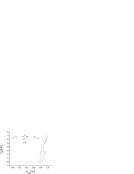
Out of the devices with measurable conduction, 24 exhibited hysteretic behavior qualitatively like that shown in Fig. 1. Additional representative curves are shown in Supporting Information, to give a sense of the device-to-device variation. The source-drain bias is swept from zero to a pre-defined endpoint (typically 1 V) in 40 s, then back to zero. Conductance is low ( S) until a characteristic threshold is reached. A discontinuous transition to a higher conductance state occurs; some devices exhibit regions of astability, in which several rapid transitions between the high and low conductance states occur, for just exceeding . At higher biases, the device remains in the high-conductance state. As the bias is swept back down, the device remains in the high-conductance state until a second characteristic bias, is reached, at which point there is a transition back to the low-conductance state. In two additional devices, hysteresis was also observed, but with the opposite sense; that is, initial sweeps began in a more conducting state and at high biases a transition was observed to a less conducting state.
Control experiments were performed using both bare junctions and electromigrated junctions incorporating dodecanethiol (). Out of a total of 145 control device subjected to the same biasing scheme, no devices exhibited this hysteretic conduction. This is consistent with the BPDN-DT molecules being responsible for the hysteresis.

Both the switching voltages and the width (in ) of the hysteretic region vary considerably from device to device. As shown in Fig. 2, ranges from 390 mV to as high as 1.7 V, but in most of these devices is around 700 mV. This correlates well with previously reported results on voltage-controlled conductance switching in BPDN-DTBlumetAl05NM . The astability near the transition points between the two conductance branches further complicates attempts to quantify the width of the hysteresis. A hysteretic device under typical bias sweep conditions survives on the order of 10 bias sweeps (all showing hysteresis) before irreversibly changing to a lower conductance, non-hysteretic configuration, though occasional devices exhibited much better stability, surviving hundreds of cycles.
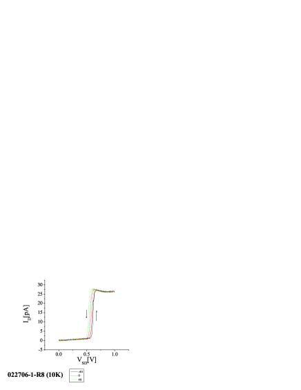
In addition to the source and drain, the BPDN-DT molecules in our devices are capacitively coupled to a gate electrode. The effective strength of this coupling depends strongly on the geometry of the junction, and the strength of the coupling between the molecule and the electrodes. In previous SMT experiments we have examined thousands of devices, and found that approximately 10-15% of the initially patterned electrodes show significant gate dependence. This is true both for physisorbed molecules (CYuetAl04NL ; YuetAl04Nanotechnology and transition metal complexes attached via gold-thiol bondsYuetAl04PRL ; YuetAl05PRL . In the BPDN-DT devices examined, only two out of the original 464 devices show any systematic gate dependence; Fig. 3 shows a set of curves from one of these devices.
Detailed studies of the gate dependence (e.g. the conductance maps as a function of and familiar from Coulomb blockade devices) were impeded by the short device lifetime described above. However, it was possible on the other gate-dependent device to sit at a bias near and sweep , to search for any systematic variation of with gate potential. The data are shown in Fig. 4. The device shows sporadic, hysteretic switching between conductance states as is varied, with a weak, nonmonotonic trend toward lower conduction at more positive . Note that this is the opposite trend as that seen in the device of Fig. 3.

These data constrain the switching mechanism discussion significantly. If the source of the hysteresis is an electronic effect such as polaron formation, one would expect a reproducible, systematic trend of with . An increasingly positive acts to stabilize additional electronic population on the molecule, presumably lowering the source-drain bias required to populate the next electronic level. The efficiency of gate coupling in previous SMT devices with this oxide thicknessYuetAl04NL ; YuetAl04PRL ; YuetAl05PRL has generally been on the order of a few percent, implying that a 100 V swing of should systematically shift molecular levels (and correspondingly and ) by a few hundred meV. Whether this is sufficient to bring a molecular level into alignment with the source/drain chemical potential depends on the details of the molecule’s electronic structure (gap between highest occupied and lowest unoccupied molecular orbitals) and the molecule-metal bonding. Further, while transport via highest occupied vs. lowest unoccupied orbitals could affect the sign of the gate trend, the differences between Figs. 3 and 4 would imply that qualitatively identical transport in different devices takes place through different orbitals, which seems unlikely.
Within the polaronic picture of hysteresis, which implies that the energetic difference between the source/drain chemical potential and a molecular orbital is , there are limited possible explanations for the observed weak gate coupling. If this particular molecule self-assembles or moves during electromigration in a manner very different than in other experiments, it is conceivable that there could be a systematic trend toward device geometries with weak gate couplings. This seems unlikely, given the relatively ordinary self-assembly properties of BPDN-DT reported by Blum et al.BlumetAl05NM . Very strong electronic coupling of the BPDN-DT molecules to at least one of the electrodes could also explain a relatively weak effect of the gate. If the molecular levels are strongly pinned relative to the Fermi level of a lead, then effectively the molecule will be screened well from the gate potential. Such a strong lead coupling would strongly constrain dynamic polaron formation, requiring weak gate coupling, yet a large enough reorganization energy that small bias-driven charge transfer could shift the level into or out of resonance, all relatively independent of the details of the Au site to which the molecule is bound. Detailed quantum chemistry calculations should at least be able to assess the likelihood of such strong coupling between the molecule and the metal, as well as the level alignments mentioned above.
A more plausible explanation, in our view, is that the switching mechanism in these devices is based on bias-driven changes in the molecule/electrode hybridization or bond angle, rather than a direct electronic process like polaron formation. The lack of gate dependence would then naturally follow from a large energetic difference between molecular levels and the source/drain chemical potential. Given the heterogeneous environment of the electromigrated junctions, it would not be surprising for the molecule to bind asymmetrically to the electrodes. Indeed, during initial SAM formation, only one end of the molecule is expected to be bound to the Au surface. Under this circumstance, the bound molecule can acquire a net electric dipole moment, which may be enhanced by the strong electron-withdrawing character of the nitro groups in BPDN-DT. STM experiments have already demonstratedLewisetAl05JACS that electric dipoles can lead to a bias influence on conductance switching in other molecules, which has been interpreted as due to changes in molecule/electrode hybridizationLewisetAl05JACS ; MooreetAl06JACS .
We have performed measurements of electromigrated junctions in a SMT configuration incorporating BPDN-DT, a molecule known from other experiments to exhibit hysteretic conductance switching as a function of . We observe similar hysteretic characteristics that are absent in control devices not incorporating the molecule of interest. The dependence of the conductance on is much weaker than observed with other molecules in SMT experiments. While not the only possibility, a likely explanation is that the switching mechanism in these devices is not charge-based, but rather depends on the geometry of the molecule/metal interface. Performing SMT experiments using molecules known to have strong polaron formation tendencies remains an interesting direction to pursue. Similarly, because polaron stability depends strongly on the electronic environment, examination of switching processes in electrochemical cells (i.e. immersed in electrolyte) are also of much interest.
DN acknowledges support from the Research Corporation, the Robert A. Welch Foundation, the David and Lucille Packard Foundation, an Alfred P. Sloan Foundation Fellowship, and NSF award DMR-0347253. JMT acknowledges support from DARPA via the AFOSR.
References
- (1) Moore, A.M.; Dameron, A.A.; Mantooth, B.A.; Smith, R.K.; Fuchs, D.J.; Ciszek, J.W.; Maya, F.; Yao, Y.; Tour, J.M.; Weiss, P.S. J. Am. Chem. Soc. 2006, 128, 1959-1967.
- (2) Blum, A.S.; Kushmerick, J.G.; Long, D.P.; Patterson, C.H.; Yang, J.C.; Henderson, J.C.; Yao, Y.; Tour, J.M.; Shashidar, R.; Ratna, B.R. Nat. Mater. 2005, 4, 167-172.
- (3) Kushmerick, J.G.; Holt, D.B.; Yang, J.C.; Naciri, J.; Moore, M.H.; Shashidar, R. Phys. Rev. Lett. 2002, 89, 086802.
- (4) Long, D.P.; Patterson, C.H.; Moore, M.H.; Deferos, D.S.; Bazan, G.C.; Kushmerick,J.G. Appl. Phys. Lett. 2005, 86, 153105.
- (5) Seminario, J.M.; Zacarias, A.G.; Derosa, P.A. J. Chem. Phys. 2002, 116, 1671-1683.
- (6) Galperin, M.; Ratner, M.A.; Nitzan, A. Nano Lett. 2005, 5, 125-130.
- (7) Alexandrov, A.S.; Bratkovsky, A.M.; Williams, R.S. Phys. Rev. B 2003, 67, 075301; Alexandrov A.S.; Bratkovsky, A.M. Phys. Rev. B 2003, 67, 235312.
- (8) Mitra, A.; Aleiner, I.; Millis, A.J. Phys. Rev. Lett. 2005, 94, 076404.
- (9) Mozyrsky, D.; Hastings, M.B.; Martin, I. Phys. Rev. B 2006, 73, 035104.
- (10) Collier, C.P.; Jeppesen, J.O.; Luo, Y.; Perkins, J.; Wong, E.W.; Heath, J.R.; Stoddart, J.F. J. Am. Chem. Soc. 2001, 123, 12632-12641.
- (11) Di Ventra, M.; Kim, S.G.; Pantelides, S.T.; Lang, N.D. Phys. Rev. Lett. 2001, 86, 288-291.
- (12) Cornil, J.; Karzazi, Y.; Brédas, J.L. J. Am. Chem. Soc. 2002, 124, 3516-3517.
- (13) Ramachandran, G.K.; Hopson, T.J.; Rawlett, A.M.; Nagahara, L.A.; Primak, A.; Lindsay, S.M. Science 2003, 300, 1413-1416.
- (14) Kornilovitch, P.E.; Bratkovsky, A.M. Phys. Rev. B 2001, 64, 195413.
- (15) Donhauser, Z.J.; Mantooth, B.A.; Kelly, K.F.; Bumm, L.A.; Monnell, J.D.; Stapleton, J.J.; Price, D.W.; Rawlett, A.M.; Allara, D.L.; Tour, J.M.; Weiss, P.S. Science 2001, 292, 2303-2307.
- (16) Lewis, P.A.; Inman, C.E.; Maya, F.; Tour, J.M.; Hutchison, J.E.; Weiss, P.S. J. Am. Chem. Soc. 2005, 127, 17421-17426.
- (17) Natelson, D. Single-molecule transistors. In Handbook of Organic Electronics and Photonics; Nalwa, H.S., Ed. American Scientific: 2006 (in press).
- (18) Park, H.; Park, J.; Lim, A.K.L.; Anderson, E.H.; Alivisatos, A.P.; McEuen, P.L. Nature 2000, 407, 57-60.
- (19) Yu, L.H.; Natelson, D. Nano Letters 2004, 4, 79-83.
- (20) Yu, L.H.; Keane, Z.K.; Ciszek, J.W.; Cheng, L.; Stewart, M.P.; Tour, J.M.; Natelson, D. Phys. Rev. Lett. 2004, 93, 266802.
- (21) Pasupathy, A.N.; Park, J.; Chang, C.; Soldatov, A.V.; Lebedkin, S.; Bialczak, R.C.; Grose, J.E.; Donev, L.A.K.; Sethna, J.P.; Ralph, D.C.; McEuen, P.L. Nano Lett. 2005, 5, 203-207.
- (22) Chae, D.-H.; Berry, J.F.; Jung, S.; Cotton, F.A.; Murillo, C.A.; Yao, Z. Nano Lett. 2006, 6, 165-168.
- (23) van der Zant, H.S.J.; Kervennic, Y.V.; Poot, M.; O’Neill, K.; de Groot, Z.; Thijssen, J.M., Heersche, H.B.; Stuhr-Hansen, N.; Bjornholm, T.; Vanmaekelbergh, D.; van Walree, C.A.; Jenneskens, L.W. Faraday Disc. 2006, 131, 347-356.
- (24) Yu, L.H.; Natelson, D. Nanotechnology 2004, 15 S517-S524.
- (25) Cai, L.; Yao, Y.; Yang, J.; Price, D. W., Jr.; Tour, J. M. Chem. Mater. 2002, 14, 2905-2909.
- (26) Park, H.; Lim, A.K.L.; Park, J.; Alivisatos, A.P.; McEuen, P.L. Appl. Phys. Lett. 1999, 75, 301-303.
- (27) Yu, L.H.; Keane, Z.K.; Ciszek, J.W.; Cheng, L.; Tour, J.M.; Baruah, T.; Pederson, M.R.; Natelson, D. Phys. Rev. Lett. 2005, 95, 256803.
- (28) Flatt, A.K.; Dirk, S.M.; Henderson, J.C.; Shen, D.E.; Su, J.; Reed, M.A.; Tour, J.M. Tetrahedron 2003, 59, 8555-8570.