Interface hole-doping in cuprate-titanate superlattices
Abstract
The electronic structure of interfaces between YBa2Cu3O6 and SrTiO3 is studied using local spin density approximation (LSDA) with intra-atomic Coulomb repulsion (LSDA+U). We find a metallic state in cuprate/titanate heterostructures with the hole carriers concentrated substantially in the CuO2-layers and in the first interface TiO2 and SrO planes. This effective interface doping appears due to the polarity of interfaces, caused by the first incomplete copper oxide unit cell. Interface-induced high pre-doping of CuO2-layers is a key mechanism controlling the superconducting properties in engineered field-effect devices realized on the basis of cuprate/titanate superlattices.
pacs:
74.81.-g,74.78.-w,73.20.-r,73.20.MfIn complex thin-film oxide heterostructures of structurally compatible but physically dissimilar compounds, interface phenomena can substantially affect the charge properties. A prominent example ohtomo is the titanate superlattice composed of insulating layers of SrTiO3 and LaTiO3, where the mixed valence (/) of Ti leads to an interface-driven electronic redistribution and to metallic conductivity. Moreover, when one of the superlattice compounds is a copper oxide film, where the high- properties can be tuned by doping, the behavior is even more intriguing. Such heterostructures consisting of YBa2Cu3O7-δ-films grown on SrTiO3-layers are of essential importance due to their applications in superconducting field effect devices mannhart . It is well established that external electrostatic fields can significantly affect the superconducting transition temperature () in these layered materials which is often understood in terms of electrostatic doping [the more charge is field-injected into the film the larger ]mannhart ; logvenov . Despite capturing the key mechanism of charge modulation in the field-effect, this concept does not include a detailed consideration of the microstructure of the YBa2Cu3O7-δ-film near the interface assuming that the latter remains unaffected by the adjacent SrTiO3 interface layer.
Several experimental facts, however, indicate an interface-related change of the electronic states in the cuprate/perovskite oxide heterostructures. First, recent experimental studies performed on the underdoped cuprate films resulted in a -shift of about 5–15 K, whereas in the overdoped films no shifts were observed, a fact, which cannot be explained satisfactorily by field-doping mannhart . Furthermore, studies of hole mobility in the CuO2 planes of SrTiO3-cuprate superlattices suggest a substantial localization of injected holes even above the hole-density level necessary for a bulk superconductor-insulator transition eckstein ; pavlenko_kopp . However, little is known about the electronic properties of the interfaces between the copper and titanium oxides. This is even more surprising considering the fact that despite the different physical properties, the structural compatibility of the cubic SrTiO3 and YBa2Cu3O7-δ makes them good candidates to assemble heterostructures and study interfacial phenomena. The electronic band insulating state of bulk SrTiO3 with a wide gap of about eV between the valence O band and empty Ti bands is reasonably well described within an LSDA approach. In contrast, the standard band theory calculations fail to describe the antiferromagnetic Mott insulating state of strongly underdoped or undoped cuprates like YBa2Cu3O6. Instead, the band properties of YBa2Cu3O6 with a gap of about eV determined by Cu and oxygen electrons can be satisfactorily treated by introducing the intra-atomic orbital dependent Coulomb repulsion for the electrons in Cu orbitals.
To provide deeper insight into the interface physics of such heterostructures, we present and interpret results of electronic structure calculations for the superlattice based on insulating YBa2Cu3O6-films and SrTiO3. As SrTiO3 consists of an alternating sequence of electrostatically neutral (001) layers, one can expect that in such heterostructures, the chemical bonding at the (001) interface with YBa2Cu3O6 will be determined by the first termination layer which can be either SrO or TiO2. It is worth pointing out that if the first unit cell of a YBa2Cu3O6-film were completely grown on the surface of SrTiO3, the interface would be electrostatically neutral. In this case, the direct influence of the interface would be essentially reduced to the small change in the band structure of YBa2Cu3O6, originating from the mismatch of the lattice constants (Å in cubic SrTiO3 versus Å in YBa2Cu3O6). However, the recent X-ray studies of interface arrangement bals ; abbamonte show clear indications of the incompletely growing unit cells of cuprate films at the SrTiO3 substrate, which may drastically change the interface electronic properties.
In this case the interface between polar layers, formed with the anisotropic YBa2Cu3O6-crystal structure, and non-polar SrTiO3 (001) planes would result in the so called “polar catastrophe” which appears on account of the divergent electrical potential wolf . The electronic compensation of the divergence can be achieved by a redistribution of the extra charge carriers near the interface which leads to a dramatical change of the electronic states in such a heterostructure. The possibility of such an electronic reconstruction has been demonstrated by Hesper et al. for a polar (111) surface of K3C60 hesper .
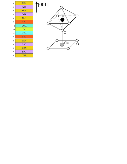
To illustrate the resulting electronic properties, we consider first a superlattice formed on the basis of a sandwich-type supercell. The YBaCuO/SrTiO-supercell shown in Fig. 1 consists of an incomplete copper oxide unit cell YBa2Cu2O6 shared between two layers, each containing 2 unit cells of SrTiO3. Effectively, the interface bonding here appears by a ‘substitution’ of the CuO chains, terminating a full YBa2Cu3O7-δ cell, with the TiO2-planes which is illustrated in the right panel of Fig. 1. Our choice of interface bonding is strongly motivated by recent TEM-studies of the YBa2Cu3O7-δ films and similar compounds grown on SrTiO3 with pulsed laser deposition technique bals . In the case, when the substrate of SrTiO3 is terminated by a TiO2-layer, the determined interface bonding arrangement is typically a stack of /SrO/TiO2/BaO/CuO2/Y/CuO2/BaO/CuO/ layers. Such structural stacks suggest an interface chemical bonding Ti-O-Cu with the oxygen of the BaO-layers shared between the CuO2 and TiO2-planes. From the electrostatical point of view, the initial ‘bulk-type’ electronic charging of the constituent layers indicated in the left panel of Fig. 1 would result in 1 extra hole which is needed in order to compensate the polarity. From the point of view of symmetry, this compensation leads to a doping of each block /SrO/TiO2/BaO/CuO2 by 0.5 hole.
To understand the redistribution of the extra charge density, which would appear near the interface, we calculated the densities of states of a YBa2Cu2O6/SrTiO3 sandwich using the linearized augmented plane wave method (LAPW) implemented in the WIEN2k package wien2k . Technical details include the SIC-variant of the LSDA+ method anisimov on a -point grid with eV and eV on the Cu orbitals. The lattice constants Å are fixed to the structural values of SrTiO3, whereas the optimized interface distance Å between the apical oxygens of BaO layers and TiO2 planes has been found by minimization of the total energy, which corresponds to Å.
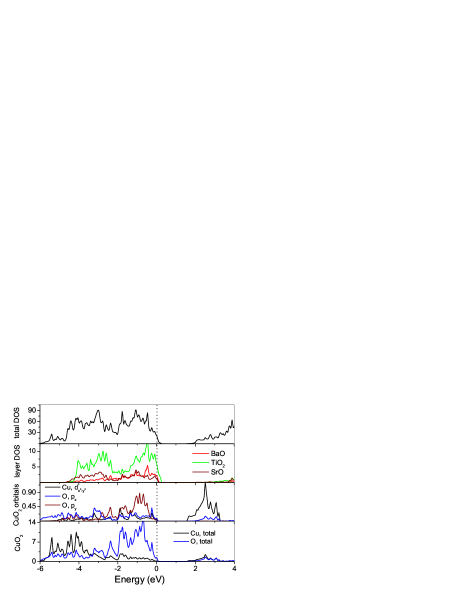

Fig. 2 shows the calculated density of states where the position of the Fermi level is indicated by dots. One can immediately identify the metallic state with hole carriers in the superlattice from the total density of states as originating from the oxygen states. We note that, similar to bulk YBa2Cu2O6, the Cu states are empty and separated by a gap of eV from oxygen 2 whereas Cu and bands remain below the Fermi level. As one can see from Fig. 2, a substantial amount of charge compensating hole density is distributed over CuO2 planes. However, we find that also BaO layers as well as the first interface TiO2 and SrO planes are doped. The upper boundaries of the O bands of the more distant SrO and TiO2 planes (with respect to the interface) remain almost on the same level with which implies that the charge is confined essentially in the interface block of SrO/TiO2/BaO/CuO2 layers. Fig. 3 shows the distribution of hole density spatially resolved along ([001])-direction within this interface block and calculated for optimized ( Å) and unrelaxed ( Å) sandwiches. To obtain this quantity, we have generated the charge density in the energy interval between the Fermi level and the top of the valence band. Specifically, we obtain that, although approximately of the hole density is located in the CuO2 planes, the major part is concentrated within the BaO () and the first TiO2 () and SrO () layers. This suggests a finite metallic conductivity in the titanate, BaO and copper oxide planes. Furthermore, while the relaxation of the structure leads to the reduction of the hole density in the BaO plane and to its redistribution within the interface SrO and more distant planes, the hole density in the CuO2 planes remains almost unaffected.
The resultant hole charge in the copper oxide planes of cuprate/titanate heterostructures clearly demonstrates that, apart from chemical doping, the interface polarity is another important mechanism which modulates the doping level in the cuprate films. In superconducting field effect devices, operated by electrostatic charging, an initial pre-doped hole density, caused by the interface, may have striking consequences on their performance. The most important feature is the shift which may be directly affected when a typically achievable hole density is injected into the already pre-doped () copper oxide film. Moreover, it appears that much higher hole doping levels including strong overdoping at the interfaces can be obtained in other interface configurations when the first unit cell of YBa2Cu3O7-δ at the interface remains incomplete.
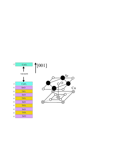
To demonstrate such a structurally induced overdoping, we consider a case in which a copper oxide plane is directily deposited on a SrTiO3 substrate terminated by SrO (Fig. 4). The direct deposition of the single Cu2+O plane on the non-polar titanate layer would require 2 extra holes to maintain the overall charge neutrality. To achieve such an extremely high doping level, interface electronic reconstruction is inevitably required. The importance of electronic reconstruction is strongly supported by significant smoothing of interference fringes observed with anomalous X-ray scattering in doped La2CuO4+δ-films—an effect explained by the mobile carrier depletion in cuprate films near the SrTiO3 substrate abbamonte . Apart from the electronic mechanism, other forms of interface reconstruction could modify the chemical composition. For example, the ionic compensation due to the cation intermixing and oxygen vacancies (oxygens missing in CuO2 during the growth) will be a competing mechanism to compensate the polarity wolf . However, it is still instructive to enforce atomically flat and stochiometric surfaces in order to investigate comprehensively the electronic mechanism multi .
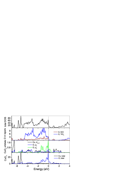
In our theoretical studies, in order to focus on the effect of electronic reconstruction, we have introduced a decoupling vacuum layer of Å thickness between the CuO2 surfaces in the superlattice of the same slab geometry, as shown in Fig. 4. Furthermore, we have optimized the superlattice structure with a relaxed distance Å between the interface CuO2 and SrO which corresponds to a total energy minimum. The electronic density of states calculated from LSDA+ is shown in Fig. 5. Here we see that the effect of hole doping is more pronounced than in the case of the YBa2Cu2O6/SrTiO3 sandwich: the energy gap between O and Cu states basically disappears and the Fermi level is located well below the top of the valence band which characterizes a metallic state with hole carriers. The hole charge is present in the CuO2 planes, where it is hybridized between the oxygen and , and Cu orbitals. Also, there is clear evidence for holes in the first SrO layer and in the next TiO2 layer of SrTiO3. In these layers, is also located below the top of the O bands.

How is the hole charge redistributed near the interface? To provide more details, we have calculated the density of holes in the planes nearest to the interface. The results in Fig. 6 show that most of the charge (about ) is confined to the CuO2 plane and a substantial amount of hole density is located in the first SrO plane (about ) and more distant TiO2 () plane. Consequently, such heavy overdoping of CuO2 should completely exclude any possibility for superconducting state in the interface unit cells of the cuprate films.
As the crystal structure of YBa2Cu3O7-δ is closely compatible with the perovskite SrTiO3, all possible basic polar interface configurations can be effectively reduced to the discussed two cases. In the first case (A) with TiO2-termination of SrTiO3, the first interface layer in the incomplete cell of YBa2Cu3O7-δ is expected to be BaO in order not to disturb the perovskite stacking. In the second case (B) with SrO termination of SrTiO3, the CuO2 layer is the most compatible for a continuous stacking (cf. Fig. 4). In both of these situations, the interface polarity leads to a hole density in CuO2 ranging from (case (A)) to (case (B)) holes per interface. In addition, due to steps and different stacking modes at the interfaces bals , one expects rather a combination of cases (A) and (B). In fact, the latter implies the formation of weak links with either connected or disconnected underdoped and heavily-overdoped regions. For such possible interface configurations, the direct consequence of the deduced pre-doping is a strong suppression of the shift related to the hole injection— or even a complete suppression of the superconductivity in few unit cells of the cuprate films.
Up to now, the growth of high-quality YBa2Cu3O7-δ-films terminated by complete unit cells remains to be a challenging task due to their roughness caused by ionic compensation of the interface polarities. In order to make a step towards perfect interfaces, where the hole injection would completely determine the superconducting dome, we need to consider other superconducting cuprates as possible candidates for non-polar interface. In this context, a proposal for field effect experiments is to grow Sr2CuO2Cl2 (SCOC) or Ca2CuO2Cl2 (CCOC) on SrTiO3. These systems can be perfectly cleaved between SrCl(CaCl)layers, and the deposition on SrTiO3 terminated by TiO2 would result in a nonpolar interface stack TiO2/SrCl/CuO2/SrCl/SrCl/ (for CCOC a similar stack with CaSr). Our LSDA-calculations for such superlattices suggest an insulating state. The lattice constants’ mismatch ( Å in SCOC) results in a slight increase () of the - hybridization integral harrison . Assuming the on-site Hubbard coupling not to be affected by strains, the direct interface effect in SCOC/SrTiO3 is a renormalization of the parameters of the effective – model zhang (, ) which would only increase , without changing the doping level. Such superlattices, where the combination of chemical doping by Na and electrostatic hole injection should not be affected by the interface pre-doping, would be ideal candidates to probe the electrostatic field effect.
This work was supported through the DFG SFB-484, BMBF 13N6918A, DAAD D/03/36760, and by the Canadian funding agencies NSERC and CIAR. The research was performed with infrastructure funded by CFI and British Columbia Knowledge Development Fund (A Parallel Computer for Compact-Object Physics). Grants of computer time from the Leibniz-Rechenzentrum München are gratefully acknowledged.
References
- (1) Also at the Institute for Condensed Matter Physics, 79011 Lviv, Ukraine.
- (2) A. Ohtomo et al., Nature 419, 378 (2002); S. Okamoto and A.J. Millis, Nature 428, 630 (2004).
- (3) J. Mannhart et al., Phys. Rev. Lett. 67, 2099 (1991); C.H. Ahn et al., Science 284, 1152 (1999).
- (4) G.Yu. Logvenov et al., Appl. Phys. Lett. 83, 3528 (2003); A. Cassinese et al., Appl. Phys. Lett. 84, 3933 (2004).
- (5) S. Oh et al., Phys. Rev. B 70, 064509 (2004); J.N. Eckstein and I. Bozovic, Annu. Rev. Mater. Sci. 25, 679 (1995).
- (6) N. Pavlenko and T. Kopp, Phys. Rev. B 72, 174516 (2005).
- (7) J.G. Wen, C. Traeholt, and H.W. Zandberger, Physica C 205, 35 (1993); S. Bals et al., Physica C 355, 225 (2001).
- (8) P. Abbamonte et al., Science 297, 581 (2002).
- (9) D. Wolf, Phys. Rev. Lett. 68, 3315 (1992); M. Kiguchi et al., Phys. Rev. B 68, 115402 (2003); C. Noguera et al., J. Phys.:Condens. Matter 16, S2509 (2004).
- (10) R. Hesper et al., Phys. Rev. B 62, 16046 (2000).
- (11) P. Blaha et al., WIEN2K, An Augmented Plane Wave + Local Orbitals Program for Calculating Crystal Properties, ISBN 3-9501031-1-2 (TU Wien, Austria, 2001).
- (12) V.I. Anisimov et al., Phys. Rev. B 48, 16929 (1993).
- (13) In the more general case when a multiplanar YBaCuO-layer terminated by CuO2 is deposited on SrTiO3, 1 extra hole is required to compensate the polarity. Despite the high doping level, such a structure will be more stable than a single CuO2 layer due to the compensating microscopic fields.
- (14) Here we use Harrison’s estimate ; see W.A. Harrison, Elementary electronic structure (World Scientific, 2004).
- (15) F.C. Zhang and T.M. Rice, Phys. Rev. Lett. 37, 3759 (1988); A. Macridin et al., Phys. Rev. B 71, 134527 (2005).