Description of self-synchronization effects in distributed Josephson junction arrays using harmonic analysis and power balance
Abstract
Power generation and synchronisation in Josephson junction arrays have attracted attention for a long time. This stems from fundamental interest in nonlinear coupled systems as well as from potential in practical applications. In this paper we study the case of an array of junctions coupled to a distributed transmission line either driven by an external microwave or in a self-oscillating mode. We simplify the theoretical treatment in terms of harmonic analysis and power balance. We apply the model to explain the large operation margins of SNS- and SINIS-junction arrays. We show the validity of the approach by comparing with experiments and simulations with self-oscillating es-SIS junction arrays.
Josephson junctions (JJs) are well known to be able to generate microwave power. Their dynamics can also phase-lock either to an external microwave bias or to the self-generated signal from an array of junctions jai1 . A common configuration is to couple a number of JJs through a distributed transmission line resonator wan1 . Both overdamped wan1 and underdamped bar1 junctions in this configuration are known to be able to mutually synchronize. Long arrays of JJs coupled to a transmission line driven by external microwave bias are known to exhibit properties, which can only be explained by the collective dynamics of the JJ-transmission line system sch1 ; has1 .
Coupled Josephson junction arrays have been modelled by semiclassical dynamical simulations caw1 ; alm1 ; fil1 ; kim1 , or in terms of lengthy perturbation analysis tsy1 . The dynamics of coupled arrays is complex making engineering of such devices challenging, often based on trial and error. However, in most practical situations it suffices to study the situation, where all the junctions are phase-locked to a driving signal (either external or self-generated). Recognizing this, we develop a simplified modelling technique. We have previously considered the case of external microwave bias, for which we calculated the gain in the limit of very small power self-generation has1 . Here we extend the analysis to the case of arbitrarily large gain, and apply it to self-stabilized overdamped JJ arrays. We analyze also the self-oscillating array by means of a power balance equation. Finally, we compare the results of the analytic model with simulations and experiments.
We assume that the tunnel element is effectively voltage biased. This is ensured by a small impednace , connected in parallel with the tunnel element (see Fig. 1(a)). Here is the critical current, is the flux quantum and is the drive frequency. We further assume that the dynamics is phase-locked to the driving signal. Below we drop the explicit -dependence from the function notation, since all the quantities are evaluated at that frequency. The condition for phase-locking (to the first Shapiro step) is kau1
| (1) |
where , and is the Bessel function of the first kind. Here is the DC bias current, is the DC resistance in parallel to the junction and is the amplitude of the driving signal.
Using the assumptions above, we get the fundamental frequency component of the Josephson current (see Fig. 1(a)) has1 . Within harmonic approximation the voltage across the tunnel element is , where the phase is referred to the driving signal . We define dynamical impedance , in series with , where is the transmission line inductance per junction length. We neglect , assuming . The effects discussed here follow from the real part . is the real part of the linear impedance parallel to the junction, and is due to the Josephson effect.
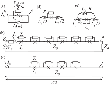
Knowing various properties of arrays are readily obtained. We consider first the case of external microwave drive (Fig. 1(b)). With the (nonlinear) attenuation per junction is
| (2) |
where is the transmission line impedance. If , the junction attenuates and if , it amplifies the driving current. This is a generalization from the theory of low-loss transmission lines (e.g. poz1 ). The current distribution along an array ( being the position of the :th junction) can be recursively obtained from . This also generalizes our previous results has1 to arbitrarily large gains.
Our second case is a resonator driven by self-generated power of the JJ:s (Fig. 1(c)). We note that the generated (or dissipated) power of a JJ at position is . The current distribution in the system can therefore be solved by means of a power balance equation
| (3) |
where the left side is the generation due to all JJ:s and is the excess loss, i.e. all power loss mechanisms not related to the junction or the shunt. In a high-Q resonator with the resonant frequency determines the generated frequency. The position dependence of depends also only on the resonator properties, whereas the overall amplitude depends on the gain and dissipation of JJ:s and on . The criterion (1) needs to be satisfied for all .
We identify two limits for in terms of junction type. The first is a resistive environment (Fig. 1(d)): at the drive frequency. This is relevant to SNS or SINIS junctions with appropriate parameters. In this case we get, using above definition and results of Ref. has1 for
| (4) |
in which is the derivative of the Bessel function.
The second limit is a capacitive environment, , which is valid for unshunted SIS junctions. The subgap leakage resistance can typically be neglected. This is also a good approximation for externally shunted SIS (es-SIS) junctions, if (Fig. 1(e)). Here is the series inductance of the shunt resistor. We get
| (5) |
where for unshunted junctions. For es-SIS junctions the losses in the shunts can be the dominant mechanism of linear dissipation, although their effect on JJ oscillation (second term in (5)) is small. For the arrangement of Fig. 1(e), if , where .
It is experimentally known that long overdamped arrays driven by external microwave compensate for the transmission line attenuation sch1 . This is the reason why SNS and SINIS Josephson voltage arrays work in spite of the huge attenuation due to intrinsic damping sch1 ; ham1 . With the above notation, self-compensation occurs if the amplitude of the propagating signal is initially between and such that (see (2), (4))
| (6) | |||||
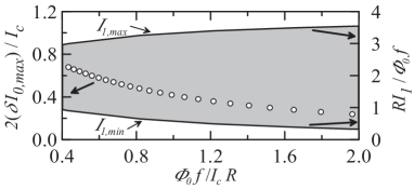
In addition, and need to satisfy (1). Then approaches the stable point towards the end of the transmission line. Fig. 2 shows the maximum step width and pump current margin , within which the array self-stabilizes the microwave current. Typical values of the design parameter of overdamped arrays vary between 0.5 and 2. In this range, the maximum self-stabilized step width varies between 0.2 and 0.6. Using the parameters of Fig. 2 in sch1 (), our model predicts A and dB, which are in excellent agreement with the exprimental data ( A and dB).
In SIS and es-SIS junctions, does not change sign as function of (see the second term in (5)). Therefore the tendency for power self-stabilization is not present. The much smaller attenuation of the capacitive environment makes phase-locking of all junctions possible in this case for a reasonable number of junctions has1 ; has2 .
Finally, to study self-oscillating arrays, we prepared arrays embedded in open-ended or microstrip resonators. The circuits were fabricated using the Nb/Al/AlOx/Nb fabrication line of VTT gro1 and measured at 4.2 K. The resonators were 800 m or 1600 m long Nb strips having a resonant frequency nominally about 80 GHz. The resonators had 2-28 es-SIS JJ:s centered around the node(s) of the standing wave. A photograph of one of the structures is shown in Fig. 3(a). Measured IV curves are shown in Fig. 3(b).
The AC current distribution in the resonators is given as . The excess loss is given as where is the total inductance of the resonator and is the intrinsic Q-value. Using Eqs. (3),(5) the power balance stands . This is solved for . For no physical solution exist, since can be negative only for positive . We get
| (7) | |||||
| (8) |
Here we have rewritten (1) for convenience. For the resistive environment also the negative side of the step appears.
The solutions for which all junctions are phase-locked to the driving signal appear in the IV curves of Fig. 3 as steps with voltage (for simplicity we omit the small dependence of on the bias point due to ). This happens for the solutions of (7) that satisfy (8) for all . Solutions where no phase locking occurs are described by a resistive IV curve determined by the shunt resistors. We assume here that these are the only types of solutions.
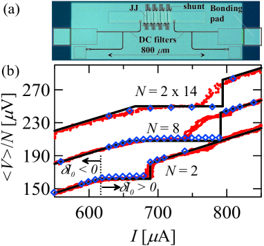
The theoretical IV curves obtained in this way are shown as solid lines in Fig. 3(b). The fitting parameters are the Q-value and the resonant frequency . The Q-value was fitted to the case with , for which the effect of the parameter spread is the smallest. The result was used for all the arrays. This corresponds to a transmission line loss of dB dB/m, very close to that of an earlier measurement (50 dB/m) has2 . The loss is dominated by the dielectric (PECVD SiO2) loss. The resonance frequencies for all devices were very close to the nominal value 80 GHz. Other parameters were obtained independently either from the IV curves or from the known circuit and material properties.
The fact that steps appear only for as expected is clarified for in Fig. 3(b). The step widths are close to the values predicted by the theory, though smaller. The difference is explained by parameter spread (the shunt resistances varied up to within a chip, changing the effective bias point by tens of A).
To further study the validity of the model we performed time-domain simulations using Stewart-McCumber model for the junctions and a distributed model of a dissipative transmission line poz1 to describe the resonator sections. We found good agreement with the analytic model. The model step widths are well reproduced, though the small bending of the plateau due to finite is not accounted for by the single-frequency model. As assumed, in all cases the numerical solutions were such that either all the junctions were synchronized or nonsynchronized. However, for simulated devices having even larger number of JJs per resonant node than our experimental devices, we found also partially synchronized states. Also in these cases the bias range of the completely synchronized state was correctly predicted by the analytic model.
In summary, we have developed a simple analytic technique for quantitative modelling of distributed JJ systems with a strong preferred frequency set by either an external RF signal or a high-Q resonance. The results clarify differences between underdamped and overdamped systems, a source of some controversy recently. The model provides an intuitive way of understanding the dynamics of phase locking and power generation in JJ arrays. The model predicts results in agreement with simulations and experiments and it can be used to engineer practical devices, such as mm-wave local oscillators and JJ voltage standards. An interesting alternative voltage standards is a JJ array with no external microwave source, locking the self-generated signal directly to a frequency reference. The power balance equation is easily generalized to externally loaded systems to calculate the power output. Other types of physical systems can be analyzed similarly. For example, the exact dual for systems described here is a distributed parallel array of quantum phase slip junctions moo1 , where the ”conductor gain” of JJ arrays is replaced by a ”dielectric gain”.
The work was partially supported by MIKES (Centre for Metrology and Accreditation), Academy of Finland (Centre of Excellence in Low Temperature Quantum Phenomena and Devices) and EU through RSFQubit (FP6-3749). The authors wish to thank Antti Manninen for useful discussions.
References
- (1) A. K. Jain, K. K. Likahrev, J. E. Lukens, and J. E. Sauvageau, Phys. Rep. 109, 310 (1984).
- (2) K. Wan, A.K. Jain, and J.E. Lukens, Appl. Phys. Lett. 54, 1805 (1989).
- (3) P. Barbara, A. B. Cawthorne, S. V. Shitov, and C.J. Lobb, Phys. Rev. Lett. 82, 1963 (1999).
- (4) H. Schulze, R. Behr, F. Mueller, and J. Niemeyer, Appl. Phys. Lett. 73, 996, 1998.
- (5) J. Hassel, P. Helistö, L. Grönberg, H. Seppä, J. Nissilä and A. Kemppinen, IEEE Trans. Instrum. Meas. 54, 632 (2005).
- (6) R. L. Kauz, and R. Monaco, J. Appl. Phys. 57, 875 (1985).
- (7) A. B. Cawthorne, P. Barbara, S. V. Shitov, C. J. Lobb, K. Wiesenfield, and A. Zangwill, Phys. Rev. B 60 (1999).
- (8) E. Almaas, and D. Stroud, Phys. Rev. B. 65, 134502 (2002).
- (9) G. Filatrella, N. F. Pedersen, C. J. Lobb, and P. Barbara, Eur. Phys. J. B 34, 3 (2003).
- (10) K.-T. Kim, M.-S.-Kim, Y. Chong, and J. Niemeyer, Appl. Phys. Lett. 88, 062501 (2006).
- (11) D. Tsygankov, and K. Wiesenfeld, Phys. Rev. E 66, 036215 (2002).
- (12) D. M. Pozar, ”Microwave Engineering”, 2nd. ed., John Wiley & Sons, inc. (1988).
- (13) C. A. Hamilton, C. J. Burroughs, S. P. Benz, and J. R. Kinard, IEEE Trans. Instrum. Meas. 46, 224 (1997).
- (14) J. Hassel, H. Seppä, L. Grönberg, and I. Suni, Rev. Sci. Instrum. 74, 3510 (2003).
- (15) L. Grönberg, J. Hassel, P. Helistö, M. Kiviranta, H. Seppä, M. Kulawski, T. Riekkinen, and M. Ylilammi, Extended abstracts of International Superconductivity Conference 2005, Noordwijkerhout, The Netherlands, O-W.04 (2005).
- (16) J. E. Mooij, and Yu. V. Nazarov, Nature Physics 2, 169-172 (2006).