-HgS Nanocrystals: Synthesis, Structure and Optical Properties
Abstract
Well-separated mercury sulfide (HgS) nanocrystals are synthesized by a wet chemical route. Transmission electron microscopy studies show that nanocrystals are nearly spherical in shape with average size of 9 nm. Grazing angle X-ray diffraction confirms that HgS nanocrystals are in cinnabar phase. Particle induced X-ray emission and Rutherford back scattering spectrometry analysis reveal HgS nanocrystals are stoichiometric and free from foreign impurities. The optical absorption measurements show two excitonic peaks corresponding to electron-heavy hole and electron-light hole transitions, which are blue shifted by 0.1 and 0.2 eV, respectively, from its bulk value, due to quantum size effect. The experimental data obtained by optical absorption measurement is simulated with a theoretical model considering the particle size distribution as Gaussian.
I Introduction
Synthesis of nanocrystals has been of considerable interest for its wide possible application in bio-sensors alivisatos , catalysis xu , light emitting devices colvin , quantum devices dabbousi ; klein etc. HgS is also known to be a technologically important material for its pronounced dichorism zallen , birefringence bond , photoelectric kreingol ; roberts and acousto-optic properties sapriel . It is interesting to note that only HgS exists in cinnabar structure (-HgS) at normal condition among all III-V and II-VI compounds zallen1 . -HgS is a wide band gap semiconductor (= 2.0 eV). Above C temperature, HgS exhibits a zinc-blende modification(-HgS) and is a narrow band gap semi-metal (= 0.5 eV).
Very scarce reports are available on nanocrystalline -HgS although considerable work has been carried out for other II-VI group semiconductor nanocrystals. There are few reports available on nanocrystalline -HgS and also on complex structures like quantum dot quantum well in which a shell of -HgS is embedded in CdS quantum dot qadri ; mews ; yeh . Attempts have been made to synthesize -HgS by Wang et al. wang using sonochemical method. The nanocrystals synthesized in this route are of irregular shape, aggregated and hava a wide size distribution.
The present work reports a cost effective wet chemical route to synthesize -HgS nanocrystals in large scale. The synthesis route is simple as it is a single step process and carried out in room temperature. Use of polymer during synthesis process helps in getting well separated nanocrystals with relatively narrow size distribution. The polymer used here is poly vinyl alcohol (PVA). It is a water soluble, transparent and high viscous polymer.
The size, phase, stoichiometry and purity of the -HgS nanocrystals are evaluated by transmission electron microscopy(TEM), Grazing angle X-ray diffraction(GXRD), Rutherford back scattering spectrometry(RBS) and Particle induced X-ray emission spectrometry(PIXE). Optical absorption spectroscopy is used to estimate the band gap as well as the crystallite size distribution.
II Experimental
The precursors used for the -HgS nanocrystal synthesis are thiourea, mercury chloride (HgCl2), ammonia and PVA. 0.001 M aqueous solution of HgCl2 and thiourea were prepared separately. Four aqueous solution of PVA is also prepared. Twenty milliliter of PVA solution is added into 20 ml of HgCl2 solution and stirred for 10 min. Twenty milliliter of thiourea solution is added in it in the same stirring condition. Addition of 50 l of 3M ammonia solution turns this transparent solution into a pale yellow colour solution due to formation -HgS nanocrystals. The experiment is done at room temperature (300K).
The mechanism of formation of HgS nanocrystals in this
chemical route is supposed to undergo the following steps:
TEM is performed using JEOL-2010 operated at 200 KeV electron beam energy. For TEM analysis, carbon coated grids are dipped into the colloidal solution and held it aloft to dry in ambient. The GXRD is performed using Philips X’Pert system using Cu line as the incident radiation. PIXE and RBS measurements are carried out using the 3 MV pelletron accelerator with and ion beam of energies 2.5 and 3.05 MeV, respectively. Optical absorption measurements is carried out by using a dual beam Szimadzu UV-3101 PC spectrophotometer with proper baseline correction. For GXRD and Optical absorption measurement colloidal solutions are dried on glass substrate. However, for PIXE and RBS colloidal solutions are dried on silicon substrate instead of glass substrate because elements present in the glass will be reflected in the spectrum and makes the analysis complicated without giving any additional information.
III Results and discussion
III.1 GXRD and TEM studies
The formation of HgS nanocrystals is confirmed from TEM. The TEM micrograph of a typical HgS nanocrystal sample is shown in the Fig. 1 and high resolution transmission electron microscopy (HRTEM) micrograph is shown in inset. HRTEM reveals well crystallinity of the nanoparticle. The interplanar distance measured to be 0.335 nm as shown in the figure. This value is same with the interplannar distance between the (1 0 1) planes of the -HgS and in good agreement with the value estimated from GXRD and TEM selected area diffraction (SAD) pattern .
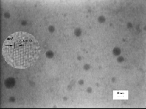

Optical properties of nanocrystals are sensitive to its shape and size. Hence, synthesis of nanocrystals with uniform shape and size, and most importantly accuracy in its measurement, is essential to derive any meaningful conclusion of its optical properties. It can be noted that the nanocrystals are nearly spherical in shape and well separated, which helps in finding the size and its distribution with a better precision. The size of several nanocrystals (700) are recorded. Nanocrystal size histogram along with the fitted Gaussian is shown Fig. 2 . The particle size distribution is best fitted with a Gaussian of 9.0 nm mean and 2.4 nm standard deviation.
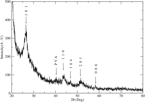
The average particle size is also calculated by analyzing the (1 0 1) peak of GXRD spectra Fig. 3. The crystallite size is calculated from Scherrer equation =/. Where is the integral breadth of the diffraction peak, is the wavelength of the incident X-ray and is the volume weighted average crystallite size. The average crystallite size calculated using above formula is 7.8 nm which is in the error limit of the value obtained from TEM analysis.
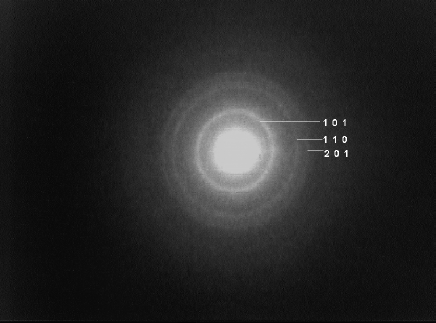
The interplannar spacing(d) obtained from the GXRD peak are in good agreement corresponding to (1 0 1), (1 1 0), (1 0 4), (2 0 1), (0 0 6) planes of the standard literature data of -HgS JCPDS . The peak at in the GXRD spectrum is due to PVAma , which plays a major role in avoiding aggregation of nanocrystals. The interpalnar spacing() is also calculated from the TEM Selected area diffraction pattern and is in good agreement to (1 0 1), (1 1 0), (2 0 1) planes. The SAD pattern is shown in Fig. 4. The continuous ring pattern indicates the polycrystallinity nature of the sample. The formula used to calculate -value in the SAD pattern is =/. where L is the Camera length, R is the Radius of the Ring and is the wavelength of the electron beam. Hence it is concluded that nanocrystals are in cinnabar phase (-HgS). -HgS belongs to space group and consists of -S-Hg-S-Hg-S- helical chains, six atoms to a turn. The chains are arranged in close packing, so that space lattice is hexagonal zallen1 . The lattice parameters in - and -axis are 4.149 and 9.495 , respectively. It is reported that some materials show a striking change in lattice parameters in nano phase yu ; lamber . However, no such change in lattice parameter is observed in the case of nanocrystalline -HgS prepared by this chemical route.
III.2 PIXE and RBS studies
Presence of any impurity in nanocrystals can change its optical properties appreciably. Hence, PIXE and RBS are used to identify the composition, stoichiometry and impurity in the HgS nanocrystals.
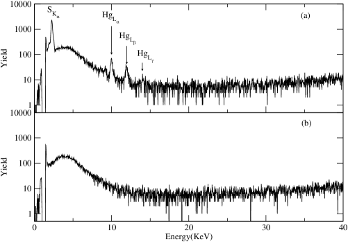
In the PIXE experiment, the multiple target holder is placed in the plane normal to the beam direction. ion beam of energies 2.5 MeV is irradiated to the sample. It knocks out electrons from the innermost shells of the atoms and X-rays are emmited with specific energies when outer shell electrons change state to inner shell. Si(Li) detector placed at with respect to the beam direction in order to detect the x-ray emitted by the de-excitation of the atoms in the sample. The beam current is kept in range of 3-5 nA in order to avoid high counting rates at the detector, as it reduces the detection sensitivity due to increase of the background noise. The PIXE spectrum was first calibrated with standard sample and then spectra for -HgS nanocrystals on silicon substrate and a bare silicon is recorded. For comparison purpose the spectra of -HgS nanocrystals on silicon substrate and a bare silicon is shown in Fig. 5. The intensity ratios and energy position of these well resolved peaks are analyzed using GUPIX-2000 software campbell . Under simulation, it is found that the peaks are coming due to the X-ray emmited from different atomic levels of mercury and sulfur. Sulfur is a light element. Hence its K X-rays are prominent but mercury being a heavy element, its L X-rays are detected. The peaks are marked as HgLα, HgLβ, HgLγ, and SKα as shown in the Fig. 5. Absence of any other peak in the spectra suggests that there is no foreign element in the sample even at the ppm level. Here it should be noted that detection of element with atomic number less than 11 is limited due to the use of Si(Li) detector in the experiment. Hence, presence of element having atomic number less than 11 in the sample can not be ruled out.
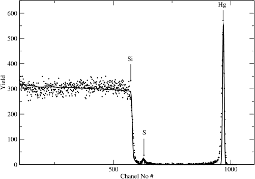
In the RBS experiment the multiple target holder is placed in the plane normal to the beam direction. The ion of energy 3.05 MeV is irradiated to the sample. Some of these ions backscatter due to ellastic collision with the atomic nuclei of the sample. The energy of these backscattered ions is related to the mass of the target element from which the ion backscatters. For the case of heavy target atoms the back scattered energy is high, for the case of light target atoms the backscattered energy is low. The energy of the backscattered ion is measured by a surface barrier detector, about 20 KeV resolution, kept at angle to the incident ion beam. The signals from the detector electronic system are in the form of voltage pulses. The height of the pulses are propertional to the energy of the backscattered ions falling on it. The pulse height analyser stores pulses of a given height in a given voltage bin or channel. The spectrum is first recorded for three known standard samples and then -HgS nanocrystals dried on silicon substrate is used for RBS data collection under the same experimental conditions.
The experimental data and the simulated profile (using GISA-3 software) is shown in Fig. 6. The channel numbers are callibrated in terms of the pulse height from the spectrum recorded for three known standard samples. Hence, there is a direct relationship between channel number and energy. The prominent peaks in the spectrum are due to backscattering of the -particle from mercury and sulfur atom of the HgS nanocrystals. The peaks obtained for mercury and sulfur in the spectra have a narrow full width at half maximum suggesting small thickness of the film. The continuous lower energy spectrum is due to the thick silicon substrate. Absence of any other peak in the RBS spectra implies no foreign impurity in the sample. The thickness of the -HgS thinfilm used for simulation is 20 nm. Under simulation, it is found that HgS nanocrystals have stoichiometry.
III.3 Optical absorption studies
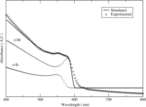
The optical absorption spectrum of a zero dimensional system is expected to have a series of isolated -function-like discrete lines. However optical absorption spectrophotometer probes a large number of nanocrystals at a time and the spectrum is the resultant of interaction of all the probed nanocrystals with light. Hence, the degree of size non-uniformity plays an important role in determining the resolvability of the individual peaks corresponding to the allowed energy level transitions and the final line shape of the spectrum. Guided by this, it is decided to simulate the experimental data to find the particle size distribution. The experimental data along with the simulated profile is shown in Fig. 7.
Following the work of Wu et al. wu absorption coefficient of a large number of cubical nanocrystals of different size with a Gaussian distribution can be written as
where two dimensionless parameters,reduced photon energy() and relative standard deviation of the nanocrystal size () is defined as follows:
and
Here is the bulk band gap, is the reduced mass of the electron-hole pair, D is the Standard deviation of the Gaussian distribution and is the optical transition dependent constant. Nanocrystals assumed cubical and is the average side length of the nanocrystals. However, -HgS nanocrystals are nearly spherical as observed from TEM measurement. Hence reduced photon energy is modified as
and
where is average diameter of the spherical nanocrystals.
The energy levels are determined by the roots of the spherical Bessel functions with being the number of the roots and being the order of the function. is the degeneracy in energy level and takes care the intensity contribution due to it.
The resolvability of peaks and the final line shape of the absorption spectrum of a quantum dot system is affected due to the contribution from both electron-heavy hole(e-hh) and electron-light hole(e-lh) transitions. The average particle size is 9.0 nm, as obtained from the TEM analysis,and Bulk band gap is 2.0 eV zallen1 . A survey of literature shows a lack of satisfactory data on the effective mass of the electron and hole of -HgS. Hence the parameters used for simulation are , , relative intensity of contribution due to electron-heavy hole and electron-light hole (I) and D. The experimental data best fits for = 0.14, = 0.07, I = 1.4 and D = 1.7 nm. Hence nanocrystal size estimated to be 9.0 1.7 nm. The standard deviation obtained under simulation is nearer but less than the value obtained from the TEM analysis. It should be noted that the number of nanocrystals probed under optical absorption spectroscopy is much larger than the number of nanoparticles analyzed under TEM. The excitonic peak corresponding to electron-heavy hole and electron-light hole transition are blue shifted 0.1 and 0.2 eV, respectively, from its bulk value due to quantum size effect.
IV Conclusion
A low cost synthesis process of well-separated -HgS nanocrystals using the chemical route is presented. Average size of the nanocrystals are 9.0 nm as determined from the TEM analysis. -HgS Nanocrystals are pure and stoichiometric. The theoretical model fits well to the experimental data of optical absorption spectroscopy and suggests a narrow size distribution of nanocrystals.
Acknowledgment
The help and constant encouragement received from Dr. S. N. Sahu, Dr. R. K. Choudhury and Dr. P. V. Satyam, Institute of Physics, are gratefully acknowledged.
References
- (1) M. Bruchez Jr., M. Moronne,P. Gin, and S. Weiss, A. P. Alivisatos, Science 281, 2013 (1998)
- (2) Z.Xu, F. S. Xiao, S. K. Purnell, O. Alexeev, S. Kawi, S. E. Deutch, and B. C. Gates, Nature 372,346 (1994)
- (3) V.L.Colvin, M. C. Schlamp, and A. P. Alivisatos, Nature 370,354(1994 )
- (4) B.O.Dabbousi, M. G. Bawendi, O. Onitsuka and M. F. Rubner, Appl. Phys. Lett. 66 , 1316 (1995 )
- (5) D. L. Klein, R. Roth, A. K. L. Lim, A. P. Alivisatos, and P. L. McEven, Nature 389,699 (1997)
- (6) R. Zallan,II-IV Semiconducting Compounds,edited by D. G. Thomas (Benjamin,New York,1967),p.877
- (7) W. L. Bond,G. D. Boyd, and H.L.Carter,J.Appl.Phys. 38,4090(1967)
- (8) F. I. Kreingol’d,Sov.Physics-solid state 4,1904(1963)
- (9) G. G. Roberts,E.L.Lind, and E. A. Davis, J. Phys. Chem. Solids 30, 833 (1969)
- (10) J. Sapriel, Appl. Phys. Lett. 19,533(1971)
- (11) R.Zallen, G.Lucovsky, W.Taylor, A.Pinczuk, and E. Burstein, Phy. Rev. B 1, 4058 (1970)
- (12) S. B. Qadri,M. Kuno,C. R. Feng, and B. B. Rath, Appl. phys. lett., 83, 4011(2003)
- (13) A.Mews, A. V. Kadavanich, U. Banin, and A. P. Alivisatos, Phys. Rev. B 53, R13242 (1996)
- (14) A. T. Yeh, G.Cerullo, U. Banin, A. Mews, A. P. Alivisatos, and C. V. Shank, Phy. Rev. B 59, 4973 (1999)
- (15) H.Wang, and J.Zhu, Ultrasonics Sonochemistry 11,293 (2004)
- (16) Joint Committee on Powder Diffraction Standards(JCPDS),File No. 42-1408
- (17) X. D. Ma, X. F. Qian, J. Yin, and Z. K. Zhu, J.Mater. Chem. 12,663 (2002)
- (18) X.F.Yu, X.Liu, K.Zhang, and Z.Q.Hu,J.Phys.:Condens. Matter 11,937 (1999)
- (19) R.Lamber,S.Wetien, and N.I.Jaeger,Phys. Rev. B 51,10968 (1995)
- (20) J.L. Campbell, T.L. Hopman, J.A.Maxwell, Z. Nezedely, Nucl. Instr. and Meth. B 170 (2000) 193
- (21) W.Y.Wu,J.N.Schulman,T.Y.Hsu,U.Efron,Appl. Phys. Lett.51,710(1987)