First principles modeling of tunnel magnetoresistance of Fe/MgO/Fe trilayers
Abstract
By carrying out density functional theory analysis within the Keldysh non-equilibrium Green’s functional formalism, we have calculated the nonlinear and non-equilibrium quantum transport properties of Fe/MgO/Fe trilayer structures as a function of external bias voltage. For well relaxed atomic structures of the trilayer, the equilibrium tunnel magnetoresistance ratio (TMR) is found to be very large and also fairly stable against small variations in the atomic structure. As a function of external bias voltage, the TMR reduces monotonically to zero with a voltage scale of about 1V, in agreement with experimental observations. We present understanding of the nonequilibrium transport properties by investigating microscopic details of the scattering states and the Bloch bands of the Fe leads.
pacs:
85.35.-p, 72.25.-b, 85.65.+hSince the prediction and elegant physics explanationzhang1 ; mathon that magnetic tunnel junction (MTJ) of Fe/MgO/Fe trilayer structure may have very high tunnel magnetoresistance (TMR), MgO based MTJ has progressed at a rapid pace in recent years and produced the highest measured TMR at room temperature: several groupsparkin1 ; yuasa reported TMR ratio in the range of 180% to 250%. TMR effect presents an excellent opportunity for spintronics, it is the key to magnetoresistive random-access-memorymoodera2 , programmable logic elementsploog , and magnetic sensors. The high TMR values in MgO based MTJs have generated great excitement for practical applications.
Atomistic calculationszhang1 ; mathon have so far played a vital role in elucidating the reason behind the observed large TMR in Fe/MgO/Fe MTJszhang1 ; mathon ; parkin1 ; yuasa . There are, however, a number of important issues remain to be understood from atomic first principles. Most existing work predictedzhang1 ; mathon TMR to be greater than 1000%, experimental data are still lower. More seriously is that experimental data on MgO based MTJs show a monotonically decreasing TMR as a function of applied bias voltageyuasa ; parkin1 and it reduces to zero when bias is about one volt. To the best of our knowledge, there have been two atomistic calculations of bias dependence of TMR for MgO barrierszhang2 ; heiliger , both used the Korringa-Kohn-Rostoker numerical technique. Ref.zhang2, predicted a substantial increase of TMR versus bias for the asymmetric system analyzed there, while Ref.heiliger, found a roughly constant TMR, a decaying TMR, or an entirely negative TMR versus bias depending on atomic structures of the interface. The origin of these differences were not clear. Earlier theorylevy on based MTJs has attributed small bias dependence of magneto-resistance to magnon scattering. Given the extreme importance of MgO based MTJ in near future spintronics and the accumulated experimental data, further quantitative understanding on quantum transport in Fe/MgO/Fe at finite bias is urgently needed.
Here we present a first principles atomistic analysis of nonlinear and non-equilibrium quantum transport in Fe/MgO/Fe MTJ. We use a state-of-the-art quantum transport techniquemcdcal ; matdcal which is based on real-space, Keldysh nonequilibrium Green’s function (NEGF) formalism combined with density functional theory (DFT). The basic idea of the NEGF-DFT formalismmcdcal is to calculate device Hamiltonian and electronic structure by DFT, populate this electronic structure using NEGF which properly takes into account nonequilibrium quantum statistics, and deal with open device boundaries directly using real-space numerical techniques. The power of NEGF-DFT methods have already been demonstrated by direct quantitative comparison to experimental datakaun1 . Our results show that for fully relaxed atomic structure of the Fe/MgO/Fe device, the equilibrium TMR ratio reaches several thousand percent—consistent with previous theoretical resultszhang1 ; kirschner . This value is also found to be fairly stable against small variations in atomic structure. We found that the TMR ratio is monotonically quenched by the bias with a scale of about one volt. The microscopic details of these transport features can be understood by the behavior of bias dependent scattering states.
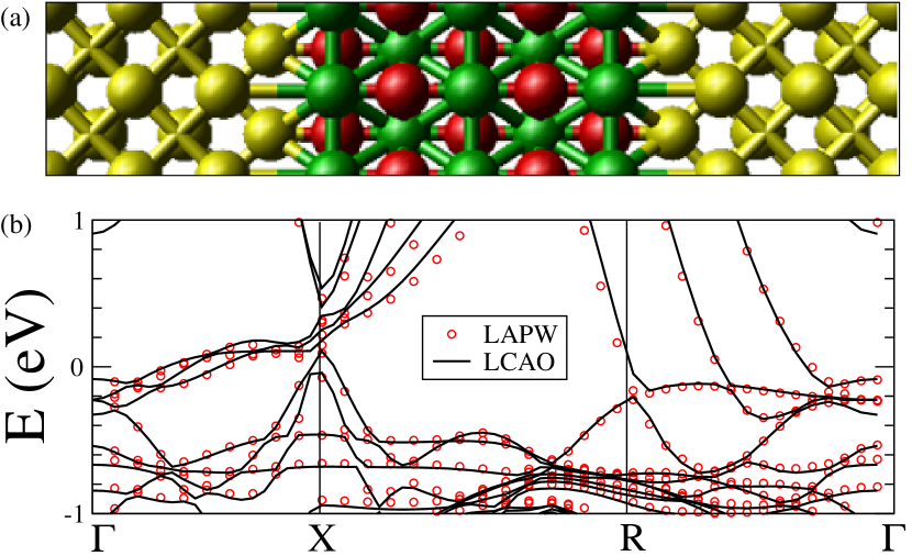
The MTJ is schematically shown in Fig.1a where a number of MgO(100) layers is sandwiched by two Fe(100) leads. The MTJ is periodic in the direction while the leads also extend to (transport direction). For DFT, we use standard norm-conserving pseudopotentialspseudopotentials and an s, p, d double-zeta LCAO basis setsiesta . The exchange-correlation potential is treated at the LSDA level. In order to accurately determine transport properties of the MTJs, we found that special care must be given to the pseudopotentials and basis sets. In our work, these inputs were carefully constructed to accurately reproduce the electronic structures of Fe, MgO, and periodic lattice of the Fe/MgO interface obtained by full potential LAPW methodLAPW . The latter comparison is shown in Fig.1b.
For the two probe MTJ simulation, we found that () points suffice to sample the 2D transverse Brillouin zone (BZ) for converging the density matrix on the complex contour energy integration in the NEGF-DFT self-consistent analysismcdcal . Much denser k-sampling of () points was required to converge the density matrix for the real energy integration of NEGFmcdcal ; matdcal and for computing the transmission coefficient by summing over the BZ: . Here is the electron energy, the external bias. The BZ resolved transmission, , is obtained by standard Green’s functions technique: , where all quantities in the trace are functions of transverse momentum. Here is the spin index; are the retarded/advanced Green’s function matrices in spin and orbital space; and are the retarded self-energies due to the existence of the bulk-3D left/right Fe leads. Finally, the spin-current (spin polarized charge current) is obtained by where is the electrochemical potential of the left/right leads. The total charge current is given by . In our calculations, the atomic structure was fully relaxed by the LAPWLAPW method between three Fe layers on each side of the MgO, with the most remote layer of Fe atoms fixed at crystalline positions during relaxation. The x-y lattice constant of the interface was fixed to our calculated one for bcc Fe, Å. The Fe-O distance was found to be Åfor a completely relaxed structure in agreement with previous studieszhang1 .
Fig.2a,b plots the current-voltage (I-V) characteristics (solid line) for 5-layer MgO device in the parallel magnetization configuration (PC) and the anti-parallel configuration (APC) of the two Fe leads, respectively. The lower insets plot the majority spin-current at small bias range. For bias less than , the total current remains extremely small. At about , the device “turns on” and current increases rapidly afterward. Such a turn-on voltage is consistent with experimental dataMgO1 ; yuasa . The spin-currents are shown as the dashed and dotted lines for the up- and down-channels (majority-, minority-channel). We found that the initial rise of the current at in PC is dominated by the down-channel where exceeds by over a factor of eight. This can be explained by investigating the transmission coefficients (see below). Above the spin-currents roughly contribute equally to the total current. The I-V curves for a 3-layer MgO device are plotted in the inset of Fig.2a,b and show similar features.
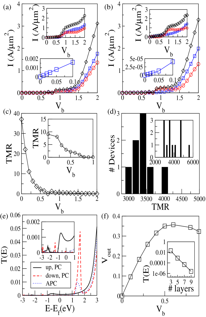
From the I-V curves we infer a TMR ratio using the common optimistic definition: , where are the total currents in APC and PC respectively. At when all currents vanish, we compute use transmission coefficientsblugel . From Fig.2c, for 5-layer MgO device % at zero bias and declines quickly with , essentially vanishes on a scale of about . For the 3-layer MgO we found % at zero bias and declines to zero with on a similar bias scale. While the experimentally measured TMR has increased dramatically in the past two yearsparkin1 ; yuasa , they are still significantly lower than theoretically predicted values here and elsewherezhang1 ; mathon . It is anticipated that surface roughness is playing a major rolexia . To investigate this effect, we generated eight device atomic structures of 5-layer MgO: for each device we varied the z-coordinates of the surface Mg and O atoms from their relaxed positions, by a random displacement corresponding to about 1% of the bond length. Self-consistent NEGF-DFT analysis is carried out for them and the result is shown in Fig.2d. Of these eight atomic structures, the minimum TMR is about 3000% while the maximum is %, with an average of 3580%. Although the sample size is small, the TMR ratio appears rather stable against small interface atom displacements. A similar analysis is carried out for thirteen 5-layer MgO devices where all the Mg and O atoms were displaced randomly by roughly 1% of the bond length, the result is in the inset of Fig.2d. Again, even though the sample size is small, the results nevertheless indicate that small random variations of atomic positions in the barrier layer are not sufficient to reduce the zero bias TMR to the presently measured experimental values. Other mechanisms such as oxidization of the Fe surface, diffusive impurities and/or defects, are likely responsible for experimental TMR values. However our results provide a theoretical upper limit which does suggest that if a device can be manufactured with a high quality interface, it may be possible to achieve even higher TMR values than presently knownyuasa .
We now investigate nonequilibrium features, namely the bias dependence of various transport properties of the MTJ. Fig.2c shows a dramatic quench of TMR by the external bias voltage with a scale of about one volt, in agreement with the experimental datayuasa ; tiusan . The origin of the TMR quenching is due to a very fast rise in the APC current relative to the PC current as a function of bias. We now analyze these features.
First, the voltage dependence of the total current and spin-current (Fig.2a,b) can be understood from the behavior of the transmission coefficient . Fig.2e plots versus electron energy at zero bias for PC and APC of the 5-layer MgO device. In PC, the majority carrier transmission (solid line) is smooth and several orders of magnitude larger than (dashed line) when is near the Fermi energy of the leads (). By analyzing the spin-dependent scattering statesmcdcal of the MTJ, we were able to determine which bands of the Fe leads contribute to the transmission. We found that is dominated by the band of the Fe leads, in agreement with Ref.zhang1, . Below , becomes extremely small due to the disappearance of the band. The , on the other hand, is considerably less smooth because the transmission near the Fermi level is mostly dominated by interface resonance statesWunnicke . In particular, a large peak in appears above : as is increased, different Fe bands may participate transport and this peak is due to such a contribution. This peak explains the much larger minority-channel current than the majority-channel current in PC at (Fig.2a), as already noted above.
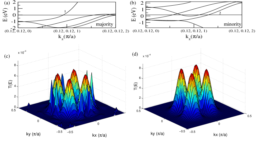
Second, for APC, we obtain for all at zero bias due to the geometrical symmetry of the device (dotted line in Fig.2e). We found that the BZ resolved total transmission, shown in Fig.3c for and Fig.3d for V, is dominated by broad and smooth peaks at around (in unit of throughout the paper, where is the Fe lattice constant mentioned above), and there is almost no transmission at . For , Fig.3c also shows that the dominating peaks are surrounded by other much sharper peaks. For APC, it is the majority channel from one Fe layer traversing the MgO barrier and going to the minority channel in the other Fe layer. Figs.3a,b plot the majority and minority electronic band structures of Fe near for , respectively. By projecting scattering states with onto the Fe bands of Fig.3a,b, the dominating peaks are found to be largely due to channel transmission: they are due to the band labelled “1” in Fig.3a at one Fe contact, transmitting to the band labelled “2” on the other Fe contact. Our calculations show that this band-to-band transmission contributes to majority channel . Other band-to-band transmissions are considerably smaller. Similarly, is mainly contributed from band-2 to band-1. Therefore, it is the band-to-band transmissions which give almost the entire hight of the dominating peaks in Fig.3c (note Fig.3c,d plot the total BZ resolved transmission)foot2 .
Third, we found that bias voltage has dramatic effects for APC. The very sharp peaks in Fig.3c, which are due to interface resonances occurring at zero bias, are completely removed by a finite bias of 0.05V, as shown in Fig.3d. Moreover, the dominating peaks become considerably higher than those in Fig.3c. We checked that even 0.01V bias can remove these sharp resonances. Again, we found that transmission from band-1 of left Fe lead to band-2 of right lead dominates, contributing to the peaks. This value is considerably larger than the value at zero bias, indicating that bias enhances the coupling of Fe bands across the MgO barrier for APC, causing a fast relative increase in the APC current as a function of bias voltage, and is responsible for quenching the TMR observed in Fig.2c.
An important parameter which has been measuredyuasa ; tiusan is the magnitude of the output signal modulation, namely with the applied bias, and are the junction resistances for APC and PC. puts more weight on information of TMR for higher bias, and is plotted as a function of bias in Fig.2f. We found that increases in a roughly linear manner and then bends over at around where is about . These voltage scales are rather similar to the experimental datayuasa ; tiusan . Finally, the inset of Fig.2f shows a semi-log plot of the zero bias total transmission at Fermi energy versus four thicknesses of the MgO barrier for PC, and the data is in perfect consistency with the physics of tunneling.
In summary, we have analyzed non-equilibrium quantum transport properties of Fe/MgO/Fe MTJs from atomic first principles without any phenomenological parameter. All the obtained voltage scales for transport features are consistent with experimental data, these include the turning on voltage for currents, voltage scale for TMR quenching, maximum value of as well as the turning over voltage of . The quench of TMR by bias is found to be due to a relatively fast increase of channel currents in APC. Very large TMR at zero bias is obtained which is stable against small changes of atomic positions. The zero bias TMR is, however, expected to be sensitive to presence or absence of impurities, oxidization layers and experimental processing procedures. It is hopeful that even greater TMR can be obtained experimentally.
Acknowledgments: We gratefully acknowledge financial support from NSERC of Canada, FRQNT of Quebec, CIAR, and Killam Research Fellowship (H.G), and NSF-China (K.X). We thank Dr. Lei Liu for assistance in several useful analysis software tools, Dr. Eric Zhu for his participation at early stages of this work, and Dr. Xiaoguang Zhang for illuminating communications on TMR physics.
References
- (1) W.H. Butler et al., Phys. Rev. B 63, 054416 (2001).
- (2) J. Mathon and A. Umerski, Phys. Rev. B 63, 220403R (2001).
- (3) S.S.P. Parkin et al., Nature Materials, 3, 862 (2004).
- (4) S. Yuasa et al., Nature Materials, 3, 869 (2004).
- (5) J.S. Moodera et al., Phys. Rev. Lett. 74, 3273 (1995); T. Miyazaki and N. Tezuka, J. Magn. Magn. Mater. 139, L231(1995).
- (6) A. Ney, C. Pampuch, R. Koch and K. H. Ploog, Nature, 425, 485 (2003).
- (7) C. Zhang et al., Phys. Rev. B 69, 134406 (2004).
- (8) C. Heiliger et al., Phys. Rev. B 72, 180406 (2005).
- (9) S. Zhang et al., Phys. Rev. Lett. 79, 3744 (1997).
- (10) J. Taylor, H. Guo and J. Wang, Phys. Rev. B. 63 245407 (2001); ibid, 63, 121104 (2001).
- (11) D. Waldron et al., Phys. Rev. Lett. 96, 166804 (2006).
- (12) C. C. Kaun, B. Larade, and H. Guo, Phys. Rev. B 67, 121411 (2003); C. C. Kaun and H. Guo, Nano Lett. 3, 1521 (2003); T. Frederiksen et al., Phys. Rev. Lett. 93, 256601 (2004); T. Lee et al. J. Phys. Chem. B 108, 8742 (2004).
- (13) C. Tusche et al., Phys. Rev. Lett 95, 176101 (2005); J.P. Velev, K.D. Belashchenko and E.Y. Tsymbal, Phys. Rev. Lett. 95, 119601 (2006).
- (14) N. Troullier and J.L. Martins, Phys. Rev. B 43, 1993 (1991).
- (15) J.M. Soler et.al., J. Phys. Condens. Matter 14, 2745 (2002).
- (16) P. Blaha, et al., WIEN2K, An Augmented Plane Wave + Local Orbitals Program for Calculating Crystal Properties, (TU Wien, Austria, ISBN 3-9501031-1-2, 2001).
- (17) W. Wulfhekel et.al., Appl. Phys. Lett. 78, 509(2001).
- (18) For a 3-layer MgO at zero bias, the majority transmission cofficient at is found to be . This value can be compared with that obtained using FLAPW and embedding Green’s function method which gave . E. Wortmann, G. Bihlmayer and S. Blügel, J. Phys. Cond. Matt. 16, S5819 (2004).
- (19) P.X. Xu et al., cond-mat/0601291.
- (20) C. Tiusan et.al., Appl. Phys. Lett. 88, 062512 (2006).
- (21) O. Wunnicke et al., Phys. Rev. B 65, 064425 (2002).
- (22) The bands in Fig.3a,b are at where the APC transmission have the broad peaks (Fig.3c,d). On the other hand, we refer bands at as band etc.. In this sense, band-1 in Fig.3a is rather like the band while band-2 of Fig.3b is like the band. Coupling between these bands in APC are possible due and due to scattering at the interfaces.