Phys. Rev. A 75, 063604 (2007)
Designing potentials by sculpturing wires
Abstract
Magnetic trapping potentials for atoms on atom chips are determined by the current flow in the chip wires. By modifying the shape of the conductor we can realize specialized current flow patterns and therefore micro-design the trapping potentials. We have demonstrated this by nano-machining an atom chip using the focused ion beam technique. We built a trap, a barrier and using a BEC as a probe we showed that by polishing the conductor edge the potential roughness on the selected wire can be reduced. Furthermore we give different other designs and discuss the creation of a 1D magnetic lattice on an atom chip.
pacs:
03.75.Be,39.90.+dI Introduction
Miniaturized atom optical elements on atom chips form the basis for robust neutral atom manipulation Fol02 ; Eur05 . The basic design idea of microscopic magnetic traps and guides is to superimpose the field of a current-carrying wire on the chip with an external bias field. Atoms are trapped in the potential minimum formed by the cancellation of the two fields. A straight wire and a homogeneous bias field give a guide for atoms Den99 , which can be transformed into a trap by changing the angle between the current flow and the bias field. The standard solution is to bend the wire. A U-shape results in a quadrupole, a Z-shape in a Joffe trap Fol02 .
In this paper we implement slight changes in the current path by sculpturing the bulk of a lithographically patterned plane conductor, as a mean to design the potential landscape. Even though this results only in minute changes of the overall current flow these are sufficient to alter significantly the local potentials for ultra-cold atoms PotSens .
II Designing Potentials
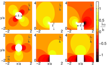
We start by looking at holes and defects in a plane conductor (fig.1). The current flow around a circular hole in a conducting sheet can be found analytically Feyn . For general structures one needs numeric calculations. For a polygonal cut in the vicinity of an edge of the conductor the Schwarz-Christoffel transformation can be used (conformal mapping Conform ). The simplest is a single step in the edge: it creates either a barrier or a trough, depending on the orientation of the dominating longitudinal field component and on the direction of the step.
The magnetic field of a general two dimensional current distribution can be evaluated in the Fourier domain. Following Roth , the current densities’ Fourier Transform components in x and y direction () are defined by:
| (1) |
and the magnetic fields’ Fourier transform:
| (2) | |||||
where the function acts as a low pass filter for . For homogeneous conductors, with independent of
| (3) |
where is the absolute value of the wave vector, the distance to the top of the current carrying surface and the thickness of the layer. At the surface of a thin conductor () .
Eq. 3 shows that the magnetic field computation can be effectively done by applying a low pass filter in Fourier space to the current distribution. This nicely illustrates the limits for potential design. In order to keep features up to a certain wave vector and to maximize their amplitude two requirements must be met:
-
•
As the contributions of the current flow pattern are exponentially damped when receding from the wire. To achieve a modulation of a fraction of the maximum achievable field at a minimum structure size one has to stay at distances
-
•
For finite thickness , the contribution of current flowing deep below the surface of the sheet starts to drop off already inside the conductor. Increasing leads to larger modulation but saturates in the limit of a thick conductor. To reach a fraction of the maximum achievable modulation, one has to satisfy
III Polishing wires
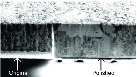
Atom Chip wires can be easily sculptured with a focused ion beam (FIB) technique, creating structures with high precision ( nanometers) and large aspect ratios (height/width) FIB . We experimentally demonstrated the power of this technique by sculpturing a wide and thick gold conductor (see fig.3 top), lithographically fabricated on a Si substrate by our standard method Gro04 ; fol00 . In our example we cut and polished the vertical faces of this wire on both edges using the FIB over a distance of .
This modification enables us to study two effects:
-
•
At the limits of the polished regions we have steps in the wire edge, as in the examples discussed above and in DPie . These steps demonstrate that small deviations in the current flow can be used to deliberately design potentials for tight traps and barriers.
- •
Figure 2 shows how the polished and the untreated edges of a gold conductor look like.
Experiments to study the potentials created by the sculptured wire were carried out in our atom chip BEC apparatus described in Sch03b . Typically atoms accumulated in a MOT are transferred to a magnetic trap created by a large wire underneath the atom chip and cooled to by RF evaporation. The resulting sample of atoms is then loaded to the selected chip trap at the desired longitudinal position, where a second stage of RF evaporation creates a pure quasi one dimensional BEC which spans typically 0.6 mm in length. The BEC is then kept for 300 ms in the trap with a close RF knife to achieve dynamic equilibrium.
We image the atomic cloud by resonant absorption imaging, with resolution. To determine the cloud distance from the surface , we incline the imaging light with respect to the chip mirror surface by ; for this leads to a double absorption image Sch03b , allowing a direct measurement of . For distances below the optical resolution the value can be extracted from the known currents and fields. To measure the atom density pictures are taken after 1.8 ms time of flight.
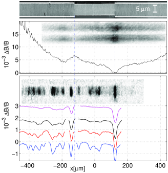
If we transfer ultra cold thermal atoms to the area where the edge is modified by the FIB we observe as dominating potential features a trap DPie and a barrier at the step of the wire edge (fig.3, center).
When cooling further, the higher atomic density in the deep potential dimple at one corner of the FIB modified area causes an enhancement of the condensate growth Stampe98 . Care has to be taken that not all atoms accumulate there. Precisely controlling the final steps of the RF cooling process we can obtain a BEC in the dimple with atom numbers ranging from to . Its longitudinal trapping frequency depends on the distance; for the set of experiments reported below we measured values in the range , with transversal confinement up to .
Using different parameters we can obtain an extended 1D-BEC. The density of such a 1D-BEC is a very sensitive measure of the potential variations at the bottom of an elongated trap and allows to deduce the magnetic field variations along the wire wild05 ; wild06 . We employed this measuring method to study the potential roughness kru05 and we use it to compare the polished section of the wire with the unpolished section.
Experiments were done with trapping currents ranging from to at an external bias field of , leading to atom-surface distances between and . Transversal confinement varied from to , longitudinal confinement was and trap bottom . Using the modulation in the observed 1D atomic density we can reconstruct the potential modulation over the whole length of the 1D BEC. Over nearly the whole range of heights, the polished section of the wire gives a smoother potential, as characterized by the rms potential roughness. For the lowest heights the full potential corrugation in the untouched region cannot be measured because it can be bigger than the chemical potential, and we exclude these data from further analysis. Comparing the standard deviation of the potential corrugations of polished section to the bare wire we find . The polished section gives nearly a factor two smoother potential, indicating a contribution of wire edge roughness Wang04 of the same order of that due to other causes.
These measurements have to be compared to previous observations of potential roughness.
Significant disorder in atom chip potentials has been reported at surface distances below when using electroplated chip wires For02 ; Lea03 ; Jon03 ; Est04 . The production process used for such chips tends to generate columnar structures along the edges of the conductors, with roughness around . As concluded in Est04 irregular current flow due to edge roughness Wang04 , is the predominant cause for the disorder potential in wires with a width of a few .
Atom chips built by lithographically patterned evaporated gold wires Gro04 on Si substrates on the contrary can show edge roughness smaller than the scale of the gold grains. The observed disorder potential in these chips can be orders of magnitude smaller and is caused by the local properties of the conductor; edge effects are negligible in many cases kru05 . These wires allow to create continuous 1D condensates at distances down to a few . The potential roughness varies from chip to chip, and even from wire to wire.
The specific wire used for these series of experiments shows a disorder potential more than a factor 10 smaller than observed in For02 ; Lea03 ; Jon03 ; Est04 ; schumm05 , but about a factor 10 larger than for the wires studied in kru05 . Our experiments indicate that edge roughness can give a contribution to disorder potential even for these lithographically patterned evaporated gold wires. In the wire studied here the contribution of the edge is of the same order of magnitude of what comes from the local properties of the metal.
To significantly decrease potential roughness the overall homogeneity of the conductor, determining the current flow also in the bulk of the wire, is the critical technological issue. We will explore this dependence in a forthcoming experiment. To fully exploit the possibilities given by the potential modulations discussed below it is however clear that wires giving trapping potentials as smooth as those seen in kru05 should be used.
In the following we give a few examples for other potentials which can be created by sculpturing the wires.
IV A double barrier potential
A short and deep cut can be seen as a structure generating a ‘current dipole’, with components perpendicular to the normal flow. As an example two deep, long cuts in opposite edges of the trapping wire give rise to a double-barrier potential, with a deep minimum in between (fig.4). For equal cuts, the double-barrier is symmetric in the wire center. Asymmetries can be introduced when moving off center. For atom transport through such a structure resonances of the atom transmission are expected, depending on the atom cloud density and on the number of bound states in the minimum DPie . In addition other non-linear effects can become dominant qtra . Inverting the relative position of the cuts changes the sign of the potential.
In correspondence with the longitudinal magnetic field modulation , variations are generated also in the other two field components, parallel to the chip surface , and perpendicular to it . They represent however a negligibly small perturbation to the local field, and are compensated by minute deviations of the trap position. For the cases considered here the displacement is smaller than the size of the ground state in the transversal harmonic potential. A detailed numerical analysis shows that the potential modulation obtained with the simple calculation, taking into account only the field along x, and the full calculation, taking into account all three field components, differ only by a few percent.
V A magnetic lattice
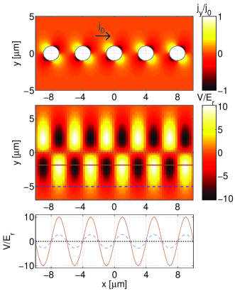
Extending the above idea, a regularly spaced set of cuts on the edge, or an array of holes in the center of a plane conductor, as illustrated in fig. 5, will create a periodic modulation of the longitudinal magnetic field, and consequently a lattice. Compared with using a thin meandering wire, periodic sculpturing of a wider wire has the advantage of resulting in a much more robust structure. Moreover it allows to create both the 1D trap and the modulation from a single setup.
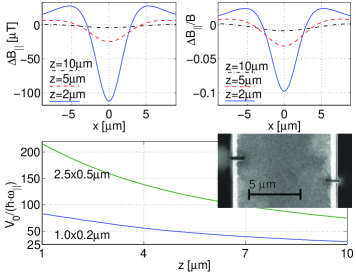
Making holes in the wire center instead of cuts in its edge gives the additional feature that the potential modulation is antisymmetric as a function of the direction transversal to the wire . The amplitude of the modulation and its phase depend on the position of the 1D trap relative to the line connecting the center of the holes. Directly above the center line the amplitude is zero. The maximum potential modulation is found at a transverse distance of about , where is the diameter of the hole (see also fig. 6). The modulation along the trap axis is to a good approximation sinusoidal; the higher Fourier components are strongly damped with height above the chip. The potential on either side of the line of holes exhibits a phase shift, but is otherwise identical. In an experiment this allows very easily to remove or invert the modulation by a transverse translation of the 1D trap.
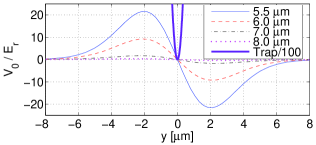
The actual peak-to-peak amplitude of the potential modulation along is plotted in fig. 6, for various heights . The convenient unit of energy to discuss these lattices is , the recoil energy associated with the lattice vector ( is the lattice period).
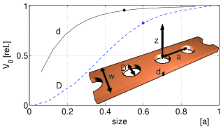
To maximize the diameter of the holes should be as big as possible (fig.7, dashed curve). In the case considered below we choose , a value at which they are still nicely separated and easy to fabricate. Keeping a constant current density, starts to saturate at a wire thickness of , as expected from eq.3. (fig.7 continuous curve).
To assess if one can observe the transition between a 1D super fluid (SF) to Mott-insulator (MI) in such a magnetic lattice we follow the work by Zwerger Zwerg03 . For a 1D system of bosons (chemical potential ) in a potential lattice the crossover from the SF to the MI regime happens at for an occupation of atoms per lattice site, where is the hopping amplitude, the on site interaction. For , . In the case of a 1D BEC of one finds in the deep lattice limit ():
| (4) |
with the scattering length kempen:02 , the trap frequency, the lattice spacing, the Gaussian ground state in the local oscillator potential. Unlike Zwerg03 the 1D nature of the trapping enters here the calculations through the 1D effective interaction strength in eq. 4, linearly dependent on .
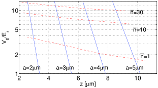
For , , and the SF-MI crossover can be achieved at (fig.8). The characteristic timescale for an experiment is given by the single particle tunnelling time; for it lies in the range of a few ms, about 2 orders of magnitude shorter than the expected lifetime at such Zhang05 ; Henkel ; Henkel1 ; Henkel2 ; Henkel3 ; Rekdal04 ; Scheel05 . The limiting factor in an experiment would be detecting the low 1D atoms’ density deteff .
Increasing up to 30 requires and the transition occurs around (fig.8, upper red dashed curve), with a single particle tunnelling time in the order of tens of ms, still about one order of magnitude shorter than the estimated lifetime and at a density experimentally observable.
The required value of at the transition can be lowered by moving deeper into the 1D regime, for example increasing ; keeping a minimum trap bottom of we can reach a confinement of . In this case the values for and used above (deep lattice) can be no longer valid. In the limit of a weak lattice, raising the transverse confinement we move into the Tonks-Girardeau (TG) regime, increasing the ratio between interaction and kinetic energy per particle: , with and Zwerg03 ; BlochTG . In the analytically solvable case of one atom per lattice site, a finite excitation gap is observable before the deep TG regime Zwerg03 . Keeping a minimum trap bottom at to avoid spin flips, and , we can achieve for ; is in this case of the same order of magnitude of .
The above estimates are rather conservative. Our atom chips Gro04 can support at least 10 times larger current densities, allowing either thinner wires resulting in a 10 times longer spin flip lifetime or much tighter confinement so that reaching should be possible.
Increasing the factor while having at the same time can lead to novel phenomena alon:05 : atoms in a MI phase can undergo a local TG-like transition in each lattice site and localize in spatially separated distributions.
VI Conclusion
We have used the characteristics of small changes in the current flow to enhance the flexibility in the design and implementation of tailored potentials for complex matter wave manipulation on atom chips. In a pilot experiment we have demonstrated engineered atom chip potentials and shown that the potential roughness can be improved by polishing the wire edge using FIB milling. These sculptured wires hold promise for many microscopic atom optical potentials on atom chips, like double wells, double barriers and magnetic lattices. An intriguing possibility is to create a potential with designed disorder or defects, combined with single site addressability and control on the atom chip.
This work was supported by the European Union, contract numbers IST-2001-38863 (ACQP), HPRN-CT-2002-00304 (FASTNet), and RITA-CT-2003-506095 (LSF), the Deutsche Forschungsgemeinschaft, contract number SCHM 1599/2-2 and the German Federal Ministry of Education and Research (BMBF) through the German-Israel Project DIP-F 2.2.
References
- (1) R.Folman, P. Kruger, J. Schmiedmayer, J. Denschlag and C. Henkel, Adv.At.Mol.Opt. Phys.48, 263 (2002)
- (2) For recent developments see the special issue: Eur.Phys.J.D 35, 1-171 (2005)
- (3) J. Denschlag, D. Cassettari and J. Schmiedmayer, Phys. Rev. Lett. 82,2014 (1999)
- (4) Ultra cold atoms are very sensitive to field variations. For in the F=2, state corresponds to 67 nK. At a bias field of this corresponds to a change in the current flow direction of rad.
- (5) The Feynman lectures on physics II, R.Feynman, R.B. Leighton and M. Sands, Chapter 12-5.
- (6) Mary L.Boas, Mathematical Methods in the Physical sciences, Wiley ed. Ch.14 Sec.10 ; for numerical solutions see also: http://www.math.udel.edu/~driscoll/SC/
- (7) B.J.Roth , Nestor G. Sepulveda and John P. Wikswo Jr., J.Appl.Phys. 65 p 361 (1989)
- (8) J.Meingailis, J.Vac.Sci.Technol.B 5 469 (1987)
- (9) Our atom chips are fabricated adapting a standard nano fabrication process. Masks written by electron beam lithography are used to structure a several thick, high quality gold layer on a Si wafer using a lift-off procedure: S. Groth et al., Appl. Phys. Lett. 85, 2980 (2004)
- (10) R. Folman et al., Phys. Rev. Lett. 84, 4749 (2000)
- (11) L.Della Pietra, S. Aigner, C. vom Hagen, H.J. Lezec and J. Schmiedmayer, J. Phys.: Conf. Ser. 19 30-33 (2005)
- (12) Daw-Wei Wang, M.D. Lukin and E. Demler, Phys.Rev.Lett. 92, 76802 (2004)
- (13) P. Krüger et al., cond-mat/0504686
- (14) S. Schneider et al., Phys. Rev. A 67, 023612 (2003)
- (15) D.M.Stamper-Kurn et al.,Phys.Rev.Lett. 81, 2194 (1998)
- (16) S. Wildermuth et al., Nature 435,440-440 (2005);
- (17) S. Wildermuth et al., Appl.Phys.Lett. 88, 264103 (2006)
- (18) J. Fortagh, H. Ott, S. Kraft, A. Günther, and C. Zimmermann, Phys. Rev. A 66, 041604(R) (2002)
- (19) A.Leanhardt et al., Phys. Rev. Lett. 90, 100404 (2003)
- (20) M. P. A.Jones, C. J. Vale, D. Sahagun, B. V. Hall and E. A. Hinds, Phys. Rev. Lett. 91, 080401 (2003)
- (21) J.Estève et al., Phys. Rev. A 70, 043629 (2004)
- (22) T.Schumm et al., Eur.Phys.J.D 32, 171 (2005)
- (23) T. Paul, K. Richter and P. Schlagheck, Phys. Rev. Lett. 94, 020404 (2005)
- (24) W.Zwerger J. Opt. B: 5 S9-S16 (2003)
- (25) E. van Kempen, S. Kokkelmans, D. Heinzen and B. Verhaar, Phys. Rev. Lett. 88 93201 (2002)
- (26) B.Zhang et al., Eur.Phys.J. D. 35, 97 (2005)
- (27) C. Henkel, M. Wilkens, Europhys. Lett. 47, 414 (1999);
- (28) C. Henkel, S. Pötting, M. Wilkens, Appl. Phys. B 69, 379 (1999);
- (29) C. Henkel, S. Pötting, Appl. Phys. B 72, 73 (2001);
- (30) C. Henkel, Eur. Phys. J. D 35, 59 (2005)
- (31) P.K. Rekdal, S. Scheel, P. L. Knight and E. A. Hinds, Phys. Rev. A. 70, 013811 (2004);
- (32) S.Scheel, P. K. Rekdal, P. L. Knight and E. A. Hinds, Phys. Rev. A. 72, 042901 (2005)
- (33) Our detection sensitivity is
- (34) B. Paredes et al., Nature 429, 277 (2004)
- (35) O.Alon, A.Streltsov and L.Cederbaum, Phys.Rev.Lett. 95, 30405 (2005)