Potential Profiling of the Nanometer-Scale Charge Depletion Layer in n-ZnO/p-NiO Junction Using Photoemission Spectroscopy
Abstract
We have performed a depth-profile analysis of an all-oxide p-n junction diode n-ZnO/p-NiO using photoemission spectroscopy combined with Ar-ion sputtering. Systematic core-level shifts were observed during the gradual removal of the ZnO overlayer, and were interpreted using a simple model based on charge conservation. Spatial profile of the potential around the interface was deduced, including the charge-depletion width of 2.3 nm extending on the ZnO side and the built-in potential of 0.54 eV.
pacs:
85.30.De, 79.60.Jv, 85.60.-qOxides are considered to expand the functions of silicon-based devices since they show a variety of magnetic, electric, dielectric, and optical properties. Innovative oxide junction devices such as transparent field-effect transistors TTFT_Prins1 ; TTFT_Prins2 ; ZnO_TTFT_Kawai ; ZnO_TTFT_Hoffman ; Nomura_TFT ; Nomura_FlexTFT ; Ginley ; Hosono_TCO , UV-light emitters Ohta_UV ; Tsukazaki , and those using correlated oxides Mathews ; Ahn_FET_super ; TanakaKawai_FET ; Muraoka ; Katsu_Photocarrier ; ZnOLSMO ; Sawa ; Ahn_OxideFET have been reported to date. The characteristic width of the charge-depletion region (CDR) at an oxide junction interface becomes as narrow as several nanometers due to the generally high carrier concentrations in carrier-doped oxides Ahn_OxideFET . Investigation of such a narrow CDR is nevertheless of primary importance since CDRs are the center of the device functions. In this Letter, we show a potential profile study of a n-ZnO/p-NiO, which is a representative and promising transparent all-oxide p-n junction diode for future oxide electronics Ohta_ZnONiO . Instead of performing a microscopy around the atomically abrupt interface between n-ZnO and p-NiO, we approached the interface by a depth-profile analysis using x-ray photoemission spectroscopy (XPS) combined with Ar-ion sputtering [Fig. 1(a)]. Since the typical photoelectron escape depth in XPS is a few nanometers ProbingDepth , depth dependent analysis with nanometer resolution became possible Handbook .
The epitaxial thin film heterostructure of ZnO(0001)/NiO:Li(111)/YSZ(111)/ITO(111) was fabricated as described elsewhere Ohta_ZnONiO . Here, NiO was p-type-doped with Li to form LixNi1-xO. ZnO thickness was 10 nm, derived from the interference fringe. Atomically flat surface and interface of the sample were confirmed by atomic force microscope [AFM: Fig. 1(b)] and high-resolution transmission electron microscope [HRTEM: Fig. 1(c)] observations. XPS measurements were performed using a Scienta SES-100 electron analyzer and an x-ray tube of Al K line ( 1486.6 eV). The energy resolution was 800 meV, and the base pressure was better than 210-10 Torr. The voltage stability was better than 5 meV during the measurements, which enabled us to determine the energy shifts with an accuracy of 40 meV albeit the rather low energy resolution of XPS. In situ sample etching was performed in the preparation chamber equipped with an ULVAC USG-3 ion gun and an Ar gas inlet. The energy and the incidence angle of the Ar-ion beam (defocused) was set 500 eV and 85∘ (grazing incidence), respectively. During the etching, the sample was moved at 0.5 Hz in the vertical direction to the incidence beam in order to ensure homogenous etching. All the measurements were performed at room temperatures.
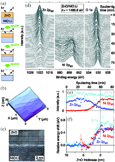
Figure 1(d) shows a series of core-level XPS spectra recorded during the removal of the initially 10 nm-thick ZnO overlayer from the ZnO/NiO:Li/ITO/YSZ sample. The binding energies are referenced to the electron chemical potential of the sample, as in usual XPS experiments. In the initial stage of sputtering (for sputtering time 30 min), one could see signals only from the ZnO overlayer. The line shapes and the energy positions of the Zn 23/2 and O 1 core-level spectra hardly changed in this stage, which confirms the reported chemical robustness of ZnO against Ar-ion sputtering Kelly . After 30 min, Ni 23/2 signals from the NiO underlayer became visible and grew its intensity, while that of Zn 23/2 gradually disappeared. The O 1 intensity remained nearly unchanged throughout, since oxygens of similar densities are present both in the ZnO over layer and the NiO under layer. At 60 min, we observed an abrupt termination of the growth of the Ni 23/2 core-level intensity. We interpreted this point as the complete removal of the ZnO layer and the exposure of NiO to the vacuum. Then, from the initial thickness of ZnO and 60 min, we could accurately determine the sputtering rate of ZnO to be 0.17 nm/min and hence the bottom axis of Fig. 1(e) and (f). The exponential rise of the Ni 23/2 intensity for 60 min was best described by the photoelectron escape depth of 1.9 nm, as shown in the theoretical curve in Fig. 1(e) 111The total intensity of the Ni 23/2 photoelectrons emitted from the NiO layer underneath the nm-thick ZnO is , where is the mean free path of Ni 23/2 photoelectrons. .
In Fig. 1(d), one can also see that the core levels were shifted toward lower binding energies during the etching, most notably in the series of the O 1 core-level spectra. The relative shifts of the core levels are plotted in Fig. 1(f). The fitted simulation curves (described below) for the shifts of O 1 and Ni 2 are also shown. One can clearly see that all the core levels suddenly started to shift toward lower binding energies at 45 min or, in terms of the ZnO thickness , at 2.5 nm. The shift continued for further sputtering until the complete removal of ZnO at 60 min.
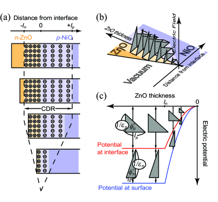
The sudden start of the core-level shifts with the kink at 2.5 nm would be understood if we consider the charge conservation in the CDR as follows. Figure 2(a) schematically shows the space-charge distributions within the CDR during the removal of the ZnO overlayer. When part of the CDR on the ZnO side is removed, the CDR on the NiO side should also shrink in order to maintain the charge neutrality. The associated changes in the electric field and electronic potential are schematically shown in Fig. 2(b) and (c). After the exposure of the CDR to the vacuum, that is, for , where is the initial CDR width on the ZnO side, both the built-in potentials in ZnO and NiO (denoted as and , respectively) start to diminish according to . Here, and are the built-in potentials initially formed on the ZnO and NiO sides, respectively. Therefore, as shown in Fig. 2(c), the potential at surface and interface does not change for , but suddenly starts to follow parabolas for .
Roughly speaking, the shift of Zn 23/2 represents the variation in the electronic potential at the surface, since the topmost contribution from the ZnO layer is the largest due to the surface sensitivity of XPS. Similarly, the Ni 23/2 shift represents the potential variation at the interface, since the contribution from the interfacial NiO layer is the largest. The simulated core-level shifts of Zn 23/2 and Ni 23/2 including the photoelectron escape depth of 1.9 nm are overlaid in Fig. 1(f). The best fit was obtained with the parameters 0.54 V (potential shift at the surface), 0.52 V (potential shift at the interface), and 2.3 nm. The extra shift of the O 1 peak compared to Zn 23/2 and Ni 23/2 is understood as the chemical shift in going from ZnO to NiO:Li.
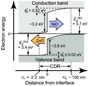
In Fig. 3, we show the band diagram across the p-n junction thus deduced. Here, the CDR width on the NiO side 1102 nm was calculated using the relationship , where DielectricZnO and DielectricNiO are the static dielectric constant ratios of ZnO and NiO, respectively [see, Fig. 2(c)]. We have also set the conduction-band minimum (CBM) of ZnO and the valence-band maximum (VBM) of NiO:Li close to , since ZnO and NiO:Li are heavily doped with electrons and holes, respectively. We adopted the optical gaps of ZnO and NiO of 3.4 eV and 3.8 eV, respectively Ohta_ZnONiO , as the band gaps. The built-in potential of 0.54 V is in good agreement with the threshold voltage 0.7 V of the diode rectifying property of n-ZnO/p-NiO Ohta_ZnONiO . The large conduction-band offset of 3 eV is in line with the large energy difference in electron affinities of ZnO and NiO BandAlignment .
The carrier concentration of ZnO and NiO:Li can be calculated from the derived parameters as cm-3 and cm-3, respectively through the relation . Here, and are the dielectric constant of the vacuum and the unit charge, respectively. The derived carrier concentration of ZnO is in reasonable agreement with the initially expected value of cm-3 Ohta_ZnONiO . The narrow CDR width of nm on the ZnO side, which corresponds to 5 unit cells of ZnO, stems from the high carrier concentration of ZnO.
So far, spectroscopic studies of the abrupt junction regions with nanometer-to-atomic resolution have been performed using cross-sectional scanning tunneling microscopy and related techniques on cleaved junction cross-sections of III-V compound semiconductor heterostructures Yu ; WolfRev ; Science . Thickness dependence analyses as demonstrated here will provide another approach in investigating the nano-scale electronic properties of the junction regions of heterostructures. Since it is not clear how far the simple semiconductor physics is applicable to the interfaces of correlated electron systems TanakaKawai_FET ; ZnOLSMO ; Ahn_OxideFET , firm understanding of their interfacial electronic structures would be necessary for further development of oxide junctions.
In summary, we have performed a depth-profile analysis of a n-ZnO/p-NiO junction using core-level XPS combined with Ar-ion sputtering. During the gradual removal of the ZnO overlayer, an onset of core-level shifts was observed at a critical ZnO thickness 2.5 nm. We described this behavior using a model based on charge conservation: the CDR shrinks from both sides of the junction when one side of the CDR is mechanically removed. We thus deduced a spatial profile of the potential around the n-ZnO/p-NiO interface, which is similar to the band diagram of a semiconductor p-n junction. The present work has demonstrated that the overlayer thickness dependence study can be used as a measure of the applicability of a semiconductor p-n junction picture to oxide-junction interfaces.
The authors acknowledge Y. Hasegawa, Y. Yuasa, S. Tanaka and A. Tsuchiya for collaboration, T. Mizokawa for discussion, K. Nomura, K. Okazaki, H. Wadati and K. Takubo for technical help. This work was supported by a Grant-in-Aid for Scientific Research in Priority Area “Invention of Anomalous Quantum Materials” from the MEXT, Japan.
References
- (1) M. W. J. Prins, K.-O. Grosse-Holz, G. Müller, J. F. M. Cillessen, J. B. Giesbers, R. P. Weening, and R. M. Wolf, Appl. Phys. Lett. 68, 3650 (1996).
- (2) M. W. J. Prins, S. E. Zinnemers, J. F. M. Cillessen, and J. B. Giesbers, Appl. Phys. Lett. 70, 458 (1997).
- (3) S. Masuda, K. Kitamura, Y. Okumura, S. Miyatake, H. Tabata, and T. Kawai, J. Appl. Phys. 93, 1624 (2003).
- (4) R. Hoffman, B. Norris, and J. Wager, Appl. Phys. Lett. 82, 733 (2003).
- (5) K. Nomura, H. Ohta, K. Ueda, T. Kamiya, M. Hirano, and H. Hosono, Science 300, 1269 (2003).
- (6) K. Nomura, H. Ohta, A. Takagi, T. Kamiya, M. Hirano, and H. Hosono, Nature 432, 488 (2004).
- (7) D. Ginley and C. Bright, MRS Bull. 25, 15 (2000).
- (8) H. Hosono, Int. J. Appl. Ceram. Technol. 1, 106 (2004).
- (9) H. Ohta, K. Kawamura, M. Orita, M. Hirano, N. Sarukura, and H. Hosono, Appl. Phys. Lett. 77, 475 (2000).
- (10) A. Tsukazaki, A. Ohtomo, T. Onuma, M. Ohtani, T. Makino, M. Sumiya, K. Ohtani, S. F. Chichibu, S. Fuke, Y. Segawa, H. Ohno, H. Koinuma, and M. Kawasaki, Nature Mat. 4, 42 (2005).
- (11) S. Mathews, R. Ramesh, T. Venkatesan, and J. Benedetto, Science 276, 238 (1997).
- (12) C. Ahn, S. Gariglio, P. Paruch, T. Tybell, L. Antognazza, and J.-M. Triscone, Science 284, 1152 (1999).
- (13) H. Tanaka, J. Zhang, and T. Kawai, Phys. Rev. Lett. 88, 027204 (2002).
- (14) Y. Muraoka and Z. Hiroi, J. Phys. Soc. Jpn. 72, 781 (2003).
- (15) H. Katsu, H. Tanaka, and T. Kawai, Appl. Phys. Lett. 76, 3245 (2000).
- (16) A. Tiwari, C. Jin, D. Kumar, and J. Narayan, Appl. Phys. Lett. 83, 1773 (2003).
- (17) A. Sawa, T. Fujii, M. Kawasaki, and Y. Tokura, Appl. Phys. Lett. 86, 112508 (2005).
- (18) C. Ahn, J.-M. Triscone, and J. Mannhart, Nature 424, 1015 (2003).
- (19) H. Ohta, M. Hirano, K. Nakahara, H. Maruta, T. Tanabe, M. Kamiya, T. Kamiya, and H. Hosono, Appl. Phys. Lett. 83, 1029 (2003).
- (20) C. Brundle, J. Vac. Sci. Technol. 11, 212 (1974).
- (21) F. Reniers, in Handbook of Surface and Interface Analysis, Methods for Problem-Solving, edited by J. C. Rivière and S. Myhra (Marcel Dekker, New York, 1998), p. 255.
- (22) R. Kelly, Nucl. Instr. Methods 149, 553 (1978).
- (23) H. Jaffe and D. Berlincourt, Proc. IEEE 53, 1372 (1965).
- (24) K. V. Rao and A. Smakula, J. Appl. Phys. 36, 2031 (1965).
- (25) H. Hosono and T. Kamiya, Bull. Ceram. Soc. Jpn. 38, 825 (2003).
- (26) E. T. Yu, Chem. Rev. 97, 1017 (1997).
- (27) P. D. Wolf, R. Stephenson, T. Trenkler, T. Clarysse, T. Hantschel, and W. Vandervorst, J. Vac. Sci. Tech. B 18, 361 (2000).
- (28) H.-K. Lyeo, A. A. Khajetoorians, L. Shi, K. P. Pipe, R. J. Ram, A. Shakouri, and C. K. Shih, Science 303, 816 (2004).