Chiral tunneling and the Klein paradox in graphene
Abstract
The so-called Klein paradox - unimpeded penetration of relativistic particles through high and wide potential barriers - is one of the most exotic and counterintuitive consequences of quantum electrodynamics (QED). The phenomenon is discussed in many contexts in particle, nuclear and astro- physics but direct tests of the Klein paradox using elementary particles have so far proved impossible. Here we show that the effect can be tested in a conceptually simple condensed-matter experiment by using electrostatic barriers in single- and bi-layer graphene. Due to the chiral nature of their quasiparticles, quantum tunneling in these materials becomes highly anisotropic, qualitatively different from the case of normal, nonrelativistic electrons. Massless Dirac fermions in graphene allow a close realization of Klein’s gedanken experiment whereas massive chiral fermions in bilayer graphene offer an interesting complementary system that elucidates the basic physics involved.
The term Klein paradox klein ; greiner ; su ; grib ; dombey ; dombey1 ; krekora usually refers to a counterintuitive relativistic process in which an incoming electron starts penetrating through a potential barrier if its height exceeds twice the electron’s rest energy (where is the electron mass and the speed of light). In this case, the transmission probability depends only weakly on the barrier height, approaching the perfect transparency for very high barriers, in stark contrast to the conventional, nonrelativistic tunneling where exponentially decays with increasing . This relativistic effect can be attributed to the fact that a sufficiently strong potential, being repulsive for electrons, is attractive for positrons and results in positron states inside the barrier, which align in energy with the electron continuum outside su ; dombey ; dombey1 . Matching between electron and positron wavefunctions across the barrier leads to the high-probability tunneling described by the Klein paradox krekora . The essential feature of QED responsible for the effect is the fact that states at positive and negative energies (electrons and positrons) are intimately linked (conjugated), being described by different components of the same spinor wavefunction. This fundamental property of the Dirac equation is often referred to as the charge-conjugation symmetry. Although Klein’s gedanken experiment is now well understood, the notion of paradox is still used widely greiner ; su ; grib ; dombey ; dombey1 ; krekora , perhaps because the effect has never been observed experimentally. Indeed, its observation requires a potential drop over the Compton length , which yields enormous electric fields greiner ; grib () and makes the effect relevant only for such exotic situations as, for example, positron production around super-heavy nuclei greiner ; grib with charge or evaporation of black holes through generation of particle-antiparticle pairs near the event horizon page . The purpose of this paper is to show that graphene - a recently found allotrope of carbon kostya1 - provides an effective medium (”vacuum”) where relativistic quantum tunneling described by the Klein paradox and other relevant QED phenomena could be tested experimentally.
DIRAC-LIKE QUASIPARTICLES IN GRAPHENE
Graphene is a single layer of carbon atoms densely packed in a honeycomb lattice, or it can be viewed as an individual atomic plane pulled out of bulk graphite. From the point of view of its electronic properties, graphene is a two-dimensional zero-gap semiconductor with the energy spectrum shown in Fig. 1a and its low-energy quasiparticles are formally described by the Dirac-like Hamiltonian slon ; semenoff ; haldane
| (1) |
where ms-1 is the Fermi velocity, and are the Pauli matrices. Neglecting many-body effects, this description is accurate theoreticallyslon ; semenoff ; haldane and has also been proven experimentallykostya2 ; kim by measuring the energy-dependent cyclotron mass in graphene (which yields its linear energy spectrum) and, most clearly, by the observation of a relativistic analogue of the integer quantum Hall effect.
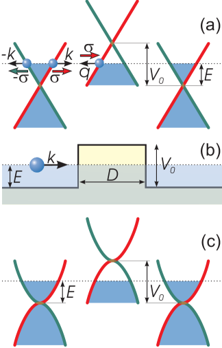
The fact that charge carriers in graphene are described by the Dirac-like equation (1) rather than the usual Schrödinger equation can be seen as a consequence of graphene’s crystal structure, which consists of two equivalent carbon sublattices A and B slon ; semenoff ; haldane . Quantum mechanical hopping between the sublattices leads to the formation of two cosine-like energy bands, and their intersection near the edges of the Brillouin zone (shown in red and green in Fig. 1a) yields the conical energy spectrum. As a result, quasiparticles in graphene exhibit the linear dispersion relation , as if they were massless relativistic particles (for example, photons) but the role of the speed of light is played here by the Fermi velocity . Due to the linear spectrum, one can expect that graphene’s quasiparticles behave differently from those in conventional metals and semiconductors where the energy spectrum can be approximated by a parabolic (free-electron-like) dispersion relation.
Although the linear spectrum is important, it is not the only essential feature that underpins the description of quantum transport in graphene by the Dirac equation. Above zero energy, the current carrying states in graphene are, as usual, electron-like and negatively charged. At negative energies, if the valence band is not full, its unoccupied electronic states behave as positively charged quasiparticles (holes), which are often viewed as a condensed-matter equivalent of positrons. Note however that electrons and holes in condensed matter physics are normally described by separate Schrödinger equations, which are not in any way connected (as a consequence of the Seitz sum rule VK , the equations should also involve different effective masses). In contrast, electron and hole states in graphene are interconnected, exhibiting properties analogous to the charge-conjugation symmetry in QEDslon ; semenoff ; haldane . For the case of graphene, the latter symmetry is a consequence of its crystal symmetry because graphene’s quasiparticles have to be described by two-component wavefunctions, which is needed to define relative contributions of sublattices A and B in quasiparticles’ make-up. The two-component description for graphene is very similar to the one by spinor wavefunctions in QED but the ’spin’ index for graphene indicates sublattices rather than the real spin of electrons and is usually referred to as pseudospin .
There are further analogies with QED. The conical spectrum of graphene is the result of intersection of the energy bands originating from sublattices A and B (see Fig. 1a) and, accordingly, an electron with energy propagating in the positive direction originates from the same branch of the electronic spectrum (shown in red) as the hole with energy propagating in the opposite direction. This yields that electrons and holes belonging to the same branch have pseudospin pointing in the same direction, which is parallel to the momentum for electrons and antiparallel for holes (see Fig. 1a). This allows one to introduce chirality haldane , that is formally a projection of pseudospin on the direction of motion, which is positive and negative for electrons and holes, respectively. The term chirality is often used to refer to the additional built-in symmetry between electron and hole parts of graphene’s spectrum (as indicated by color in Fig. 1) and is analogous (although not completely identical semenoff ; npb ) to the chirality in three-dimensional QED.
KLEIN PARADOX REFORMULATED FOR SINGLE-LAYER GRAPHENE
Because quasiparticles in graphene accurately mimic Dirac fermions in QED, this condensed matter system makes it possible to set up a tunneling experiment similar to that analyzed by Klein. The general scheme of such an experiment is shown in Fig. 1, where we consider the potential barrier that has a rectangular shape and is infinite along the y-axis:
| (2) |
This local potential barrier inverts charge carriers underneath it, creating holes playing the role of positrons, or vice versa. For simplicity, we assume in (2) infinitely sharp edges, which allows a direct link to the case usually considered in QED klein ; greiner ; su ; grib ; dombey ; dombey1 ; krekora . The sharp-edge assumption is justified if the Fermi wavelength of quasiparticles is much larger than the characteristic width of the edge smearing, which in turn should be larger than the lattice constant (to disallow Umklapp scattering between different valleys in graphene) ando . Such a barrier can be created by the electric field effect using a thin insulator or by local chemical doping kostya1 ; kostya2 ; kim . Importantly, Dirac fermions in graphene are massless and, therefore, there is no formal theoretical requirement for the minimal electric field to form positron-like states under the barrier. To create a well-defined barrier in realistic graphene samples with a disorder, fields routinely used in experiments kostya1 ; kim should be sufficient, which is eleven orders of magnitude lower than the fields necessary for the observation of the Klein paradox for elementary particles.
It is straightforward to solve the tunneling problem sketched in Fig. 1b. We assume that the incident electron wave propagates at an angle with respect to the axis and then try the components of the Dirac spinor and for the Hamiltonian in the following form:
| (6) | |||||
| (10) |
where is the Fermi wavevector, and are the wavevector components outside the barrier, is the refraction angle, , . Requiring the continuity of the wavefunction by matching up coefficients , we find the following expression for the reflection coefficient
| (11) |
Fig. 2a shows examples of the angular dependence of transmission probability calculated using the above expression. In the limit of high barriers , the expression for can be simplified to
| (12) |
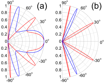
Equations (4,5) yield that under resonance conditions , the barrier becomes transparent (). More significantly, however, the barrier remains always perfectly transparent for angles close to the normal incidence . The latter is the feature unique to massless Dirac fermions and directly related to the Klein paradox in QED. One can understand this perfect tunneling in terms of the conservation of pseudospin. Indeed, in the absence of pseudospin-flip processes (such processes are rare as they require a short-range potential, which would act differently on A and B sites of the graphene lattice), an electron moving to the right can be scattered only to a right-moving electron state or left-moving hole state. This is illustrated in Fig. 1a, where charge carriers from the ”red” branch of the band diagram can be scattered into states within the same ”red” branch but cannot be transformed into any state on the ”green” branch. The latter scattering event would require the pseudospin to be flipped. The matching between directions of pseudospin for quasiparticles inside and outside the barrier results in perfect tunneling. In the strictly one-dimensional case, such perfect transmission of Dirac fermions has been discussed in the context of electron transport in carbon nanotubes ando ; mceuen (see also ref. [19]). Our analysis extends this tunneling problem to the two-dimensional (2D) case of graphene.
CHIRAL TUNNELING IN BILAYER GRAPHENE
To elucidate which features of the anomalous tunneling in graphene are related to the linear dispersion and which to the pseudospin and chirality of the Dirac spectrum, it is instructive to consider the same problem for bilayer graphene. There are both differences and similarities between the two graphene systems. Indeed, charge carriers in bilayer graphene have parabolic energy spectrum as shown in Fig. 1c, which means they are massive quasiparticles with a finite density of states at zero energy, similar to conventional nonrelativistic electrons. On the other hand, these quasiparticles are also chiral and described by spinor wavefunctions bilayer ; falko , similar to relativistic particles or quasiparticles in single-layer graphene. Again, the origin of the unusual energy spectrum can be traced to the crystal lattice of bilayer graphene with four equivalent sublattices falko . Although “massive chiral fermions” do not exist in the field theory their existence in the condensed matter physics (confirmed experimentally bilayer ) offers a unique opportunity to clarify the importance of chirality in the relativistic tunneling problem described by the Klein paradox. In addition, the relevant QED-like effects appear to be more pronounced in bilayer graphene and easier to test experimentally, as discussed below.
Charge carriers in bilayer graphene are described by an off-diagonal Hamiltonian bilayer ; falko
| (13) |
which yields a gapless semiconductor with chiral electrons and holes having a finite mass . An important formal difference between the tunneling problems for single- and bi- layer graphene is that in the latter case there are four possible solutions for a given energy . Two of them correspond to propagating waves and the other two to evanescent ones. Accordingly, for constant potential , eigenstates of Hamiltonian (13) should be written as
| (14) |
where
To find the transmission coefficient through barrier (2), one should set for for and satisfy the continuity conditions for both components of the wavefunction and their derivatives. For the case of an electron beam that is incident normally () and low barriers (over-barrier transmission), we obtain both outside and inside the barrier, and the chirality of fermions in bilayer graphene does not manifest itself. In this case, scattering at the barrier (2) is the same as for electrons described by the Schrödinger equation. However, for any finite (even in the case ), waves localized at the barrier interfaces are essential to satisfy the boundary conditions.
The most intriguing behavior is found for , where electrons outside the barrier transform into holes inside it, or vice versa. Examples of the angular dependence of in bilayer graphene are plotted in Fig. 2b. They show a dramatic difference as compared with the case of massless Dirac fermions. There are again pronounced transmission resonances at some incident angles, where approaches unity. However, instead of the perfect transmission found for normally-incident Dirac fermions (see Fig. 2a), our numerical analysis has yielded the opposite effect: Massive chiral fermions are always perfectly reflected for angles close to .
Accordingly, we have analyzed this case in more detail and found the following analytical solution for the transmission coefficient :
| (15) |
where subscripts 1,2 label the regions outside and inside the barrier, respectively. Particularly interesting is the case of a potential step, which corresponds to a single junction. Eq (15) shows that such a junction should completely reflect a normally-incident beam (). This is highly unusual because the continuum of electronic states at the other side of the step is normally expected to allow some tunneling. Furthermore, for a single junction with , the following analytical solution for any has been found:
| (16) |
which again yields for . This behavior is in obvious contrast to single-layer graphene, where normally-incident electrons are always perfectly transmitted.
The perfect reflection (instead of the perfect transmission) can be viewed as another incarnation of the Klein paradox, because the effect is again due to the charge-conjugation symmetry (fermions in single- and bi-layer graphene exhibit chiralities that resemble those associated with spin 1/2 and 1, respectively) bilayer ; falko . For single-layer graphene, an electron wavefunction at the barrier interface matches perfectly the corresponding wavefunction for a hole with the same direction of pseudospin (see Fig. 1a), yielding . In contrast, for bilayer graphene, the charge conjugation requires a propagating electron with wavevector to transform into a hole with wavevector (rather than ), which is an evanescent wave inside a barrier.
COMPARISON WITH TUNNELING OF NONCHIRAL PARTICLES
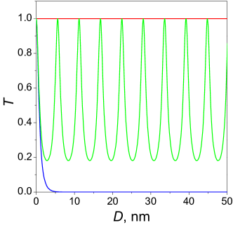
For completeness, we compare the obtained results with the case of normal electrons. If a tunnel barrier contains no electronic states, the difference is obvious: the transmission probability in this case is well known to decay exponentially with increasing barrier’s width and height esaki so that the tunnel barriers discussed above would reflect electrons completely. However, both graphene systems are gapless, and it is more appropriate to compare them with gapless semiconductors having nonchiral charge carriers (such a situation can be realized in certain heterostructures meyer ; teissier ). In this case, one finds
| (17) |
where and are -components of the wave vector outside and inside the barrier, respectively. Again, similarly to the case of single- and bi-layer graphene, there are resonance conditions at which the barrier is transparent. For the case of normal incidence () the tunneling coefficient is then an oscillating function of tunneling parameters and can exhibit any value from 0 to 1 (see Fig. 3). This is in contrast to graphene, where is always 1, and bilayer graphene, where for sufficiently wide barriers . This makes it clear that the drastic difference between the three cases is essentially due to different chiralities or pseudospins of the quasiparticles involved rather than any other feature of their energy spectra.
IMPLICATIONS FOR EXPERIMENT
The found tunneling anomalies in the two graphene systems are expected to play an important role in their transport properties, especially in the regime of low carrier concentrations where disorder induces significant potential barriers and the systems are likely to split into a random distribution of p-n junctions. In conventional 2D systems, strong enough disorder results in electronic states that are separated by barriers with exponentially small transparency ziman ; lifshitz . This is known to lead to the Anderson localization. In contrast, in both graphene materials all potential barriers are relatively transparent ( at least for some angles) which does not allow charge carriers to be confined by potential barriers that are smooth on atomic scale. Therefore, different electron and hole “puddles” induced by disorder are not isolated but effectively percolate, thereby suppressing localization. This consideration can be important for the understanding of the minimal conductivity observed experimentally in both single-layer kostya2 and bilayer bilayer graphene.
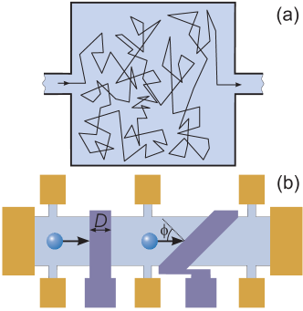
To elucidate further the dramatic difference between quantum transport of Dirac fermions in graphene and normal 2D electrons, Fig. 4a suggests a gedanken experiment where a diffusive conductor is attached to ballistic one-dimensional leads, as in the Landauer formalism. For conventional 2D systems, transmission and reflection coefficients through such a conductor are sensitive to detailed distribution of impurities and a shift of a single impurity by a distance of the order of can completely change the coefficients meso . In contrast, the conservation of pseudospin in graphene strictly forbids backscattering and makes the disordered region in Fig. 4a always completely transparent, independent of disorder (as long as it is smooth on the scale of the lattice constant ando ). This extension of the Klein problem to the case of a random scalar potential has been proven by using the Lippmann-Schwinger equation (see the Supplementary Information). Unfortunately, this particular experiment is probably impossible to realize in practice because scattering at graphene’s edges does not conserve the pseudospin ando ; berry . Nevertheless, the above consideration shows that impurity scattering in the bulk of graphene should be suppressed as compared to the normal conductors.
The above analysis shows that the Klein paradox and associated relativistic-like phenomena can be tested experimentally using graphene devices. The basic principle behind such experiments would be to employ local gates and collimators similar to those used in electron optics in 2D gases optics1 ; optics2 . One possible experimental setup is shown schematically in Fig. 4b. Here, local gates simply cross the whole graphene sample at different angles (for example, and ). Intrinsic concentrations of charge carriers are usually low ( cm-2), whereas concentrations up to cm-2 can be induced under the gated regions by the bipolar electric field effect kostya1 . This allows potential barriers with heights up to eV and eV for single- and double-layer samples, respectively. By measuring the voltage drop across the barriers as a function of applied gate voltage, one can analyze their transparency for different . Our results in Fig. 2 show that for graphene the barrier should exhibit low resistance and no significant changes in it with changing gate voltage. In comparison, the barrier is expected to have much higher resistance and show a number of tunneling resonances as a function of gate voltage. The situation should be qualitatively different for bilayer graphene, where local barriers should result in a high resistance for the perpendicular barrier and pronounced resonances for the barrier.
Furthermore, the fact that a barrier (or even a single junction) incorporated in a bilayer graphene device should lead to exponentially small tunneling current can be exploited in developing graphene-based field effect transistors (FET). Such transistors are particularly tempting because of their high mobility and ballistic transport at submicron distances kostya1 ; kostya2 ; kim . However, the fundamental problem along this route is that the conducting channel in single-layer graphene cannot be pinched off (because of the minimal conductivity), which severely limits achievable on-off ratios for such FETs kostya1 and, therefore, the scope for their applications. A bilayer FET with a local gate inverting the sign of charge carriers should yield much higher on-off ratios.
OUTLOOK
We have shown that the recently found two carbon allotropes provide an effective medium for mimicking relativistic quantum effects. On the one hand, this allows one to set up such exotic experiments as the one described by the Klein paradox and could be useful for analysis of other relevant QED problems. On the other hand, our work also shows that the known QED problems and their solutions can be applied to graphene to achieve better understanding of transport properties of this unique material that is interesting from the view point of both fundamental physics and applications.
Acknowledgements. We are grateful to Antonio Castro Neto, Vladimir Fal’ko, Paco Guinea and Dmitri Khveshchenko for illuminating discussions. This work was supported by EPSRC (UK) and FOM (Netherlands).
References
- (1) Klein, O. Die Reflexion von Elektronen an einem Potentialsprung nach der relativistischen Dynamik von Dirac. Z. Phys. 53, 157-165 (1929).
- (2) Greiner, W., Mueller, B., and Rafelski, J. Quantum Electrodynamics of Strong Fields (Springer, Berlin, 1985).
- (3) Grib, A. A., Mamayev, S. G., and Mostepanenko, V. M., Vacuum Effects in Strong Fields (Friedmann, St.-Petersburg, 1994).
- (4) Su, R. K., Siu, G. C., and Chou, X. Barrier penetration and Klein paradox. J. Phys. A 26, 1001-1005 (1993).
- (5) Dombey, N., and Calogeracos, A. Seventy years of the Klein paradox. Phys. Rep. 315, 41-58 (1999).
- (6) Calogeracos, A., and Dombey, N. History and physics of the Klein paradox. Contemp. Phys. 40, 313-321 (1999).
- (7) Krekora, P., Su, Q., and Grobe, R. Klein paradox in spatial and temporal resolution. Phys. Rev. Lett. 92, 040406 (2004).
- (8) Page, D. N. Hawking radiation and black hole thermodynamics. New J. Phys. 7, 203 (2005).
- (9) Novoselov, K. S., Geim, A. K., Morozov, S. V., Jiang, D., Zhang, Y., Dubonos, S. V., Grigorieva, I. V., and Firsov, A. A. Electric field effect in atomically thin carbon films. Science 306, 666-669 (2004).
- (10) Slonczewski, J. C. and Weiss, P. R. Band structure of graphite. Phys. Rev. 109, 272 (1958).
- (11) Semenoff, G. W. Condensed-matter simulation of a three-dimensional anomaly. Phys. Rev. Lett. 53, 2449-2452 (1984).
- (12) Haldane, F. D. M. Model for a quantum Hall effect without Landau levels: Condensed-matter realization of the “parity anomaly”. Phys. Rev. Lett. 61, 2015-2018 (1988).
- (13) Novoselov, K. S., Geim, A. K., Morozov, S. V., Jiang, D., Katsnelson, M. I., Grigorieva, I. V., Dubonos, S. V. and Firsov, A. A. Two-dimensional gas of massless Dirac fermions in graphene. Nature 438, 197-200 (2005).
- (14) Zhang, Y., Tan, Y. W., Stormer, H. L. and Kim, P. Experimental observation of the quantum Hall effect and Berry’s phase in graphene. Nature 438, 201-204 (2005).
- (15) Vonsovsky, S. V. and Katsnelson, M. I. Quatum Solid State Physics (Springer, Berlin, 1989), Sect. 4.6.6.
- (16) Boyanovsky, D., Blankenbecler, R., and Yahalom, R. Physical origin of topological mass in 2+1 dimensions. Nucl. Phys. B 270, 483-505 (1986).
- (17) Ando, T., Nakanishi, T., and Saito, R. Berry’s phase and absence of back scattering in carbon nanotubes. J. Phys. Soc. Japan 67, 2857-2862 (1998).
- (18) McEuen, P. L., Bockrath, M., Cobden, D. H., Yoon, Y. G., and Louie, S. G. Disorder, pseudospins, and backscattering in carbon nanotubes. Phys. Rev. Lett. 83, 5098-5101 (1999).
- (19) Tworzydlo, J., Trauzettel, B., Titov, M., Rycerz, A., Beenakker, C.W.J. Quantum-limited shot noise in graphene. cond-mat/0603315.
- (20) Novoselov, K. S., McCann, E., Morozov, S. V., Falko, V. I., Katsnelson, M. I., Zeitler, U., Jiang, D., Schedin, F., and Geim, A. K. Unconventional quantum Hall effect and Berry’s phase of 2 in bilayer graphene. Nature Phys. 2, 177-180 (2006).
- (21) McCann, E., and Falko, V. I. Landau-level degeneracy and quantum Hall effect in a graphite bilayer. Phys. Rev. Lett. 96, 086805 (2006).
- (22) Esaki, L. New phenomenon in narrow germanium para-normal-junctions. Phys. Rev. 109, 603-604 (1958).
- (23) Meyer, J. R., Hoffman, C. A., Bartoli, F. J., and Rammohan, L. R. Type-II quantum-well lasers for the midwavelength infrared. Appl. Phys. Lett. 67, 757-759 (1995).
- (24) Teissier, R., Finley, J. J., Skolnick, M. S., Cockburn, J.W., Pelouard, J. L., Grey, R., Hill, G., Pate, M. A., and Planel, R. Experimental determination of Gamma-X intervalley transfer mechanisms in GaAs/AlAs heterostructures. Phys. Rev. B 54, 8329-8332 (1996).
- (25) Ziman, J. M. Models of Disorder (Cambridge Univ. Press, Cambridge, 1979).
- (26) Lifshitz, I. M., Gredeskul, S. A., and Pastur, L. A. Introduction to the Theory of Disordered Systems (Wiley, New York, 1988).
- (27) Lee, P.A., Altshuler, B.L., and Webb, R. A. (Editors), Mesoscopic Phenomena in Solids (North-Holland, Amsterdam, 1991).
- (28) Berry, M. V., and Mondragon, R. J. Neutrino billiards - Time reversal symmetry-breaking without magnetic fields. Proc. Roy. Soc. (London) A 412, 53-74 (1987).
- (29) Spector, J., Stormer, H. L., Baldwin, K. W., Pfeiffer, L. N., and West, K. W. Electron focusing in 2-dimensional systems by means of an electrostatic lens. Appl. Phys. Lett. 56, 1290-1292 (1990).
- (30) Dragoman, D., and Dragoman, M. Optical analogue structures to mesoscopic devices. Prog. Quantum Electron. 23, 131-188 (1999).