Single-Walled Carbon Nanotubes as Shadow Masks for Nanogap Fabrication
Abstract
We describe a technique for fabricating nanometer-scale gaps in Pt wires on insulating substrates, using individual single-walled carbon nanotubes as shadow masks during metal deposition. More than 80 % of the devices display current-voltage dependencies characteristic of direct electron tunneling. Fits to the current-voltage data yield gap widths in the 0.8 – 2.3 nm range for these devices, dimensions that are well suited for single-molecule transport measurements.
Electronic devices based on single aromatic molecules have raised considerable interest in the last few years, as a variety of new techniques now make it possible to fabricate metal leads – separated by only a few nanometers – that can be bridged by a single molecule ebeam ; park99 ; reichert02 . Nevertheless, in spite of considerable improvements, these popular nanofabrication techniques produce gap junctions that are relatively rough at the nm scale. Electromigration, for example, is known to give rise to fairly disordered gaps containing metal islands or clusters hatzor05 , which make conductance data difficult to interpret. This issue imposes serious limits on interpreting current-voltage data obtained with such devices, as single-molecule transport experiments ideally require a large number of clean and similar metal junctions, and electron transport through organic molecules appears to be extremely sensitive to the geometry of the molecule-metal contact ratner05 .
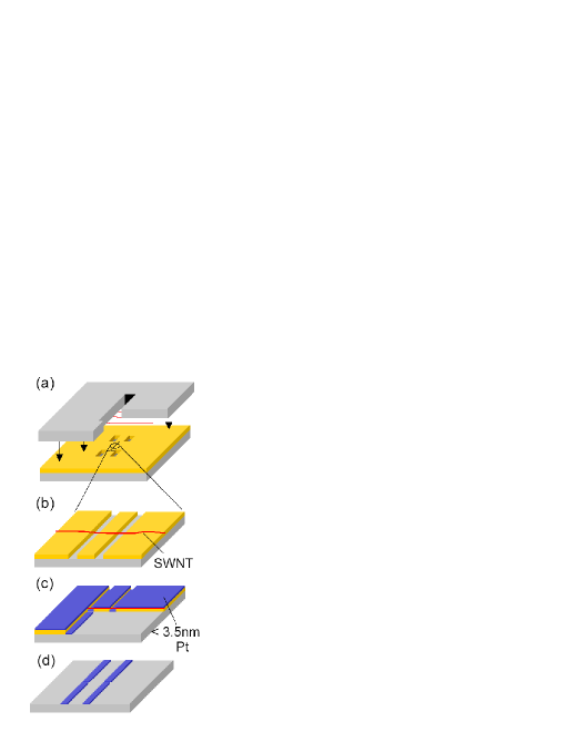
In this Letter we report a nanogap fabrication technique based on a single-walled nanotube (SWNT) shadow mask, in which the dimension of the junction is controlled solely by the diameter of the nanotube and by its distance from the substrate during metal deposition. This scheme has been applied in the past with thicker multi-walled carbon nanotubes or SWNT bundles lefebvre00 to create 20 nm-wide gaps. Here we rely on a mechanical transfer technique developed by Huang et al. xmhhuang05 to place long, quasi parallel, individual SWNT’s onto a surface patterned with an electron-beam resist film. In this way, a given nanotube is suspended over up to ten parallel “trenches” in the patterned resist; after metal deposition and lift-off, the method thus gives rise to ten nanoscale gaps defined by the same nanotube. We measure the current-voltage characteristics of 79 wires produced with this method, and deduce from tunneling data that 66 of these have widths in the 0.8 – 2.3 nm range. Only two out of 79 wires are shorted.
The metal and substrate materials we choose for wire fabrication are Pt and ZrO2, respectively. This choice is inspired by reports that the growth of Pt films over clean cubic ZrO2(100) crystals is two-dimensional roberts91 ; dilara95 , in contrast to the typical grain-like growth of noble metals on oxides campbell97 . This layer-by-layer film growth allows us, in principle, to work with metal films much thinner than those used traditionally for this type of device, which are typically about tens of nm thick PtonSi . Using ultrathin metal films allows us in turn to reduce the thickness of the resist film, and therefore to reduce the nm-scale broadening of features caused by the finite size of the metal source during Pt evaporation. Very importantly, thin Pt films also result in shallower junctions whose structure and contents could be observed by scanning probes.
The devices are made from n-doped Si substrates, coated with 3.7 nm or 9.1 nm-thick ZrO2 films formed by atomic layer deposition (ALD). We first use standard electron-beam lithography to pattern long, narrow trenches in a resist bilayer resist , developed in a 1:3 H2O:isopropanol cosolvent at 4oC with ultrasonic agitation. On a separate Si “carrier” chip, long SWNT’s are grown by chemical vapor deposition, using ethanol as carbon feedstock, according to a technique detailed in xmhhuang05 . These wafers contain 100 m x 1 mm window slits over which typically 4–10 carbon nanotubes rest suspended after growth.
We then transfer the nanotubes from their carrier chip onto the Si/ZrO2/resist sample by bringing the two samples into contact xmhhuang05 [Fig. 1(a)]. The suspended part of the nanotubes on the carrier chip adheres to the resist on the Si/ZrO2 sample, and remains on it when the two samples are separated, breaking away from the other nanotube sections [Fig. 1(b)]. The slit on the carrier sample can be easily aligned with the resist trenches under the microscope, so that the nanotubes, once transferred on the resist, are now suspended above the trenches. This method allows us currently to transfer 1–4 nanotubes from a carrier chip, though this number can probably be increased by minimizing particulate density on the samples or by reducing the total contact area between carrier and resist samples bundles .
Following the nanotube transfer, we deposit 3.5 nm Pt onto the patterned sample by electron-beam evaporation at 0.2 – 0.4 Å/s. We note that the design of the evaporation chamber and of the metal source are critical for nm-scale gap fabrication, since wide sources or short evaporation distances can taper the edges of the deposited metal by a few nm. Our Pt source is about 5 mm wide, and the source-to-sample distance 75 cm in our process. Given these dimensions, the nanotube shadow width may be reduced by up to 0.2 nm lefebvre00 , much less than the diameter of the smallest SWNT. After metal deposition, the sample is placed in boiling acetone for two hours and dipped in an ultrasound bath for 30 s in the same solvent. These steps ensure the removal of both resist and nanotubes, as well as that of the metal in the unpatterned areas.
A potential problem with this technique is that of nanotube sagging, which can cause the tubes to adhere to the oxide surface exposed at the bottom of the trenches, and ultimately prevent these tubes from lifting off properly after metal evaporation. We designed the trenches to be 35 nm deep and 40 – 200 nm wide, and were able to lift off easily all nanotubes transferred on these samples, indicated that this is not an issue for our samples.
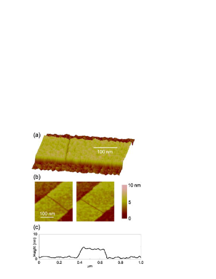
Figure 2 shows atomic force microscope (AFM) scans of some of our devices. A narrow, continuous groove cuts across the Pt wire, a result of the shadow evaporation of the metal around the suspended nanotube. The gap width is difficult to determine precisely from AFM scans because of the finite size of the scanning tip, but can be inferred from measurements of the tunneling current across the gap, as detailed below, and shown to be smaller than 2.5 nm. Several gaps are produced in this fashion from each nanotube, suspended across a sequence of parallel trenches. The resulting gaps are shown for two Pt wires in Fig. 2(b).
The linescan of the metal line [Fig. 2(c)] shows that the apparent roughness of the Pt film is comparable to that of the underlying oxide, indicating that the film, in spite of its small thickness, can form a continuous layer on ZrO2. Film continuity is also confirmed by conductance measurements, discussed below.
We study electrical transport through these wires and gaps in air and at room temperature. Wire thicknesses are about 3.5 nm for three of our devices, and about 2.5 nm for the fourth one, and the uncut wires we measured are 90 m long and 40 – 100 nm wide. 3.5 nm-thick wires have a total resistance of 0.6 – 1.2 M, i.e., 700 /square [see inset of Fig. 3(a)] 2nm . We note that these resistances, although in the M range, are small relative to typical resistances of metal-molecule-metal bridges salomon03 , and can be further reduced by appropriate design. We then study a total of 79 wires interrupted by nanogaps, and show data for four of these in Fig. 3(a). 66 of these wires show electron transport characteristic of direct tunneling, while the I-V traces are linear – and hence the gaps shorted – in only two out of the 79 wires. The remaining 11 gaps carry a current smaller than about 10 pA at 2 V bias. In contrast, most wires produced during the same process, but not shadowed by SWNT’s, do not show tunneling I-V’s.

We analyze the I-V’s of all 66 “tunneling” wires by fitting our data to Simmons’ model simmons63 , taking into account the influence of the image charge within the gap. In this model, gap width, barrier height and tunneling area are fitting parameters modelnote . Data and calculated curves for some of the devices are plotted in Fig. 3(a). We obtain gap widths ranging from 0.8 to 2.30.2 nm, with a median gap width smaller than 2 nm barrierheight . A histogram of these data is shown in Fig. 3(b). We note that these widths are consistent with the measured diameter range of the nanotubes used in our process, 0.8 nm – 1.8 nm, obtained from Raman scattering data lhuang05 .
In summary, we have developed a technique for creating thin nanoscale metal junctions, whose widths are controlled by the diameter of a SWNT shadow mask. The yield of gaps in the tunneling range (0.8 – 2.3 nm here) is larger than 80%, and less than 3% of the devices are shorted, indicating that the gaps are likely free of metal clusters. In addition, this technique helps to avoid e-beam resist contamination issues at the metal gap, a potential problem with direct electron-beam lithography. These devices are thus well suited for single-molecule transport measurements, which require excellent control over gap fabrication at the nanometer scale. Finally, the 2.5 – 3.5 nm metal thickness used in our process opens up the possibility of imaging with scanning probes single-molecule devices based on these metal films.
We thank Evgeni Gusev for the ALD growth, and Philip Kim for access to the AFM. We also thank Henry Huang for helpful discussions about the nanotube transfer technique. This work was supported by the Nanoscale Science and Engineering Initiative of the National Science Foundation under NSF Award Number CHE-0117752, by the NSF grant PHY-0103552, by the New York State Office of Science, Technology, and Academic Research (NYSTAR), and by a grant from the W. M. Keck Foundation.
aCenter for Electron Transport in Molecular Nanostructures, Columbia University, New York, NY 10027
References
- (1) C. R. K. Marrian and D. M. Tennant, J. Vac. Sci. Technol. A 21, S207 (2003); S. J. Wind (unpublished).
- (2) H. Park, A. K. L. Kim, A. P. Alivisatos, J. Park, and P. L. McEuen, Appl. Phys. Lett. 75,301 (1999).
- (3) J. Reichert, R. Ochs, D. Beckmann, H. B. Weber, M. Mayor, and H. v. Löhneysen, Phys. Rev. Lett. 88, 176804 (2002).
- (4) A. de Picciotto, J. E. Klare, C. Nuckolls, K. Baldwin, A. Erbe, and R. L. Willett, Nanotechnology 16, 3110 (2005).
- (5) H. Basch, R. Cohen, and M. A. Ratner, Nano Lett. 5, 1668 (2005).
- (6) J. Lefevbre, M. Radosavljević, and A. T. Johnson, Appl. Phys. Lett. 76, 3828 (2000).
- (7) X. M. H. Huang, R. Caldwell, L. Huang, S. C. Jun, M. Huang, M. Y. Sfeir, S. P. O’Brien, and J. Hone, Nano Lett. 5, 1515 (2005).
- (8) S. Roberts and R. J. Gorte, J. Phys. Chem. 95, 5600 (1991).
- (9) P. A. Dilara and J. M. Vohs, J. Phys. Chem. 99, 17259 (1995).
- (10) C. T. Campbell, Surf. Sci. Rep. 27, 1 (1997).
- (11) Although we did not attempt this procedure with SiO2 substrates, other groups have patterned narrow gaps using Pt deposited directly on different oxides. See, e.g., A. N. Pasupathy et al. [Nano Lett. 5, 203 (2005)] for work on Pt/Al2O3 devices. The technique described in the present paper may well be applicable to Si/SiO2 substrates or to other dielectrics, perhaps using thicker Pt (or Au) films and Ti/Cr adhesion layers, but we did not test this.
- (12) The lower layer is a MMA/8.5/MAA EL1.5 copolymer, and the upper layer 495K PMMA A1. Total resist thickness is about 35 nm.
- (13) Rayleigh scattering measurements [see M. Y. Sfeir et al., Science 306, 1540 (2004)] allow us to check that most of the suspended nanotubes on the carrier chip are unbundled, though some do form pairs or triplets.
- (14) The 2.5 nm-thick wires were approximately six times more resistive than the 3.5 nm-thick ones, although the former were measured after an acryl strip cleaning step, which likely oxidizes part of the Pt.
- (15) A. Salomon, D. Cahen, S. Lindsay, J. Tomfohr, V. B. Engelkes, and C. D. Frisbie, Adv. Mater. 15, 1881 (2003).
- (16) J. G. Simmons, J. Appl. Phys. 34, 1793 (1963).
- (17) In principle, electrons tunnel through both air and the underlying ZrO2 substrate, though additional simulations show that the oxide carries a much smaller direct tunneling current than air. In practice, we simplify the model by assuming that only one “effective” material, with a relative permittivity equal to 1, separates the electrodes.
- (18) The barrier height parameters that best fit our data vary between 4 and 6 eV. This energy variation probably results from the sensitivity of the metal work function to adsorbed gases.
- (19) L. M. Huang, B. White, M. Y. Sfeir, M. Huang, X. M. H. Huang, S. J. Wind, J. Hone, and S. O’Brien, to appear in J. Phys. Chem B.