Multiple 0 - transitions in SIFS Josephson tunnel junctions
Abstract
We report on experimental studies of superconducting coupling through a thin Ni76Al24 film. A new patterning process has been developed, which allows in combination with the wedge shaped deposition technique the in situ deposition of 20 single Nb/Al/Al2O3/Ni3Al/Nb multilayers, each with its own well defined Ni3Al thickness. Every single multilayer consists of 10 different sized Josephson junctions, showing a high reproducibility and scaling with its junction area. Up to six damped oscillations of the critical current density against F-layer thickness were observed, revealing three single 0--transitions in the ground state of Josephson junctions. Contrary to former experimental studies, the exponential decay length is one magnitude larger than the oscillation period defining decay length. The theoretical predictions based on linearized Eilenberger equations result in excellent agreement of theory and experimental results.
pacs:
74.25.Ha, 74.50.+r, 01.30.RrIn the past few years there was a noticeable interest to the unconventional Josephson junctions Gol04 ; Bu04 ; Ber05 , in particular, to the so-called - junctions having negative critical current. These junctions provide a - shift in the ground state and were realised experimentally in SFS (superconductor-ferromagnet-superconductor) and some HTS structures.
The intensive experimental study of “0” –“” transition in SFS Josephson junctions Ry03 ; Se03 ; Blu04 ; Su02 ; Be02 ; She06 ; Obo05 ; Kon02 ; Wei05 ; Se04 confirms the existence of critical current oscillations upon the thickness of ferromagnetic interlayer . Different structure of SFS sandwiches and SIFS tunnel junctions having been fabricated up to now. They contain regions which are controlling the critical current and difficult to control in experiment and describe in theory. They are SF interfaces, dead layers, and the region in S banks with suppressed superconductivity. Contrary to that the bulk properties of F material can be better controlled and well described by theoretical models based on quasiclassical theory of superconductivity. These theories predict that for large thickness of ferromagnet the critical current of SFS junctions have to exhibit a damped oscillations as a function of
| (1) |
Here is the position of the first minima, is the first experimental value of . These two values take into account the resultant action of SF interfaces and their vicinities. The oscillations are characterized by two effective lengths. They are the decay length , and the length which determines the period of oscillations. In dirty limit the expressions for follow from the Usadel equations Bu92 and have the form
| (2) |
where and are the diffusive coefficient and exchange field of ferromagnetic material, respectively. In the clean limit one can easily get from Eilenberger equations that Eil81
| (3) |
where is the electron mean free path and vF is the Fermi velocity in a ferromagnet.
It is clearly seen from Eqs. (2) and (3) that for dirty materials , and in the limit of large exchange energy, , the characteristic lengths are nearly equal . In the clean limit these and are completely independent.
Our analysis of both the bulk properties of ferromagnet materials Ku06 and the experimental data Ry03 ; Se03 ; Blu04 ; Su02 ; Be02 ; She06 ; Obo05 ; Kon02 ; Wei05 ; Se04 has shown (see Table 1) that in dilute ferromagnets Se03 ; Be02 ; Obo05 ; Kon02 the electron mean free path is very small providing the fulfilment of the dirty limit conditions for the F interlayer. In these experiments as it follows from Eq. (2). Contrary to that, in the structures with Ni interlayer the relation between and is just the opposite so that more complex model Ber01 should be used for the data interpretation. It is necessary to point out that in all previous experiments (except Se04 ) the structures were not fabricated in one run, so that the certain degree of non-reproducibility of magnetic constants of F materials occurred for junctions with different . This results in increase of spread of data with increasing and did not permit to observe the large amount of oscillations.
| Ref. | (nm) | (nm) | F-material | (m/s) | Eex(K) |
|---|---|---|---|---|---|
| [8] | 1.2 | 1.6 | Fe20Ni80 | 1100 | |
| [11] | 1.8 | 2 | Pd0.9Ni0.1 | 400 | |
| [10] | 1.2 | 3.5 | Cu0.53Ni0.47 | 850 | |
| [5] | Cu0.52Ni0.48 | ||||
| [9] | 1.7 | 1 | Ni | 2300 | |
| this work | 4.6 | 0.45 | Ni3Al | 1000 |
In this work, we improved the reproducibility of the junction parameters by preparing the structures in one run with F - layer thickness between 10 nm and 20 nm. For the first time, we succeeded in observation of up to six damped oscillations of critical current with F - layer thickness. To do this we have used the ”wedge” shaped F - layer technique and a new ferromagnetic material (Ni3Al). We experimentally obtained a one order of magnitude difference between and which is consistent with theory based on the Eilenberger equations Eil81 .
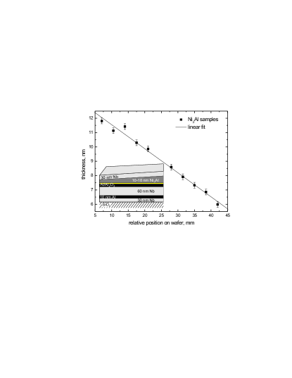
The bottom electrode of SIFS samples consists of Nb/Al/Nb/Al and was deposited on oxidized 2 inch Si wafers with argon magnetron sputtering. The top 10 nm thick Al layer has been oxidized for 2 minutes in a 0,1 mbar pure oxygen. The following Ni3Al interlayer was sputtered with neon gas from one single target. The target composition of the alloy was determined by Rutherford Backscattering (RBS) and is Ni74Al26. A 30 nm Nb top layer was deposited in situ to prevent the interlayer from oxidation. A schematic cross section of the deposited multilayer is shown in insert of Fig. 1. To achieve a thickness - gradient of the Ni3Al layer the position of the target above the substrate has been shifted during deposition for several centimeter. This permits us to produce a rather linear thickness gradient over the whole 2 inch substrate (see Fig. 1).
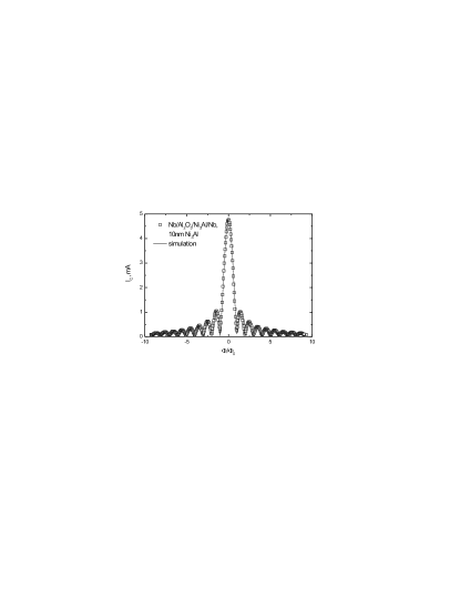
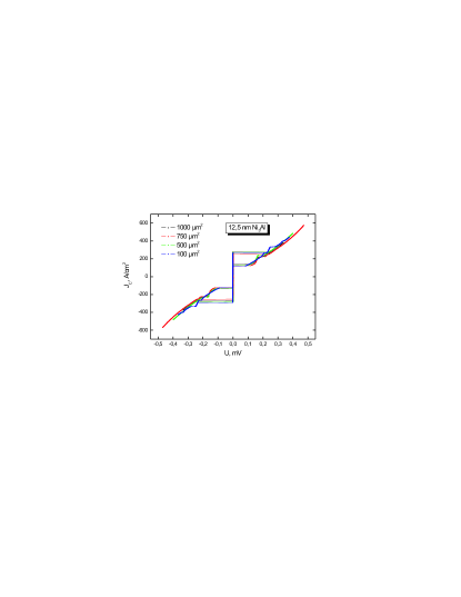
The transport measurements were performed at 4,2 K. Figure 2 shows the dependence of the critical current, , upon external magnetic field . The rather optimal agreement between experimental results and the Fraunhofer function fit indicates a uniform and homogenous current distribution in the junction. The current-voltage characteristics (CVC) of several Josephson junctions can be seen in Fig. 3. They show a clear superconducting tunnelling behaviour with a hysteresis in its curves. These four curves belong to one defined Ni3Al layer thickness of 12.5 nm. The current is normalized to the current density, since the four junctions differ in their sizes. It can be seen in Fig. 3, that the current density differs only several percent, thus showing a good reproducibility of our junctions. This result also indicates that within one patterned line the F - layer thickness variation could be neglected.The thickness gradient has been characterized and proofed with RBS measurements.
The variations are several Angstroms. We developed a patterning process that allows the creation of 20 different separated 500 m wide lines, distributed homogeneous along the F - layer thickness gradient over the 2 inch wafer. Each lines consists of 10 different sized circular Josephson junctions. The junction area differs from 5 to 1000 m2. The variation of F - layer thickness inside an individual junction is negligible small. The ferromagnetic properties of Ni3Al films depend on neon pressure. Details will be published elsewhere Bo06 . The magnetic properties of the Ni3Al layers were measured with a SQUID - magnetometer. The Curie temperature for a 250 nm thick Ni3Al layer is 74 K.
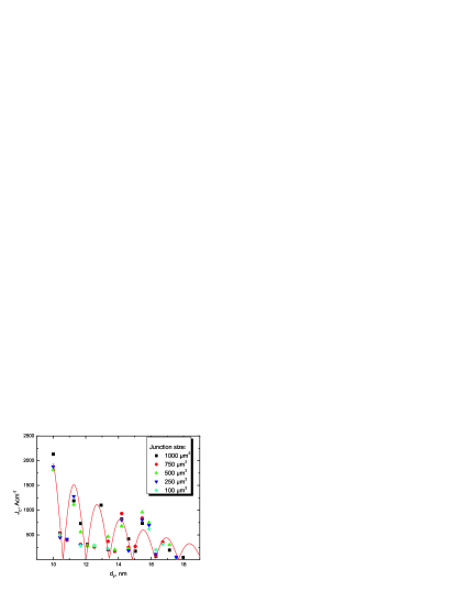
The Ni3Al thickness dependence of the critical current density can be seen in Fig. 4. Several Josephson junctions of each line were measured and plotted versus their corresponding Ni3Al-layer thickness. A clear oscillating behavior of the critical current density of more than 60 single junctions versus dF is shown, indicating three different 0 - transitions. The amplitude of oscillations decays exponentially with a characteristic decay length of =4.6 nm. It should be pointed out that the corresponding oscillation period, given by , is one magnitude smaller, namely =0.45 nm. There is a rather good agreement of the theoretical fit after Eq. (1) with these two decay length’s, see solid line in Fig. 4. The magnetically dead layer has been measured for different interfaces. Corresponding to this SIFS multilayer, we achieved a thickness of the dead layer around 5 nm to 8 nm for each interface. So, we expected the first oscillation period at around 10 nm or even more. To find a theoretical explanation for the large difference between and we start with linearized Eilenberger equations which are valid at the distances from SF interface larger than
| (4) |
Here is the angle between direction of the Fermi velocity and
interface normal, is the scattering time.
The solution of this equation has the form Ku81
| (5) |
where is the effective decay length which is independent on and is an integration constant. Substitution of Eq. (5) into Eq. (4) gives
| (6) |
Integration of Eq. (6) over angle provides the equation for
| (7) |
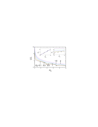
In the dirty limit, and in the clean limit the solution of Eq. (7) reduces to Eqs. (2) and (3), respectively. The results of numerical solution of Eq. (7) are presented in Fig. 5.
There are steps on and vs dependencies (see Fig. 5) accompanied by the minima on curves (see Fig. 5, right inset). The ratio of falls very rapidly with increase of . It follows from Fig. 5 that the experimental value of this ratio can be achieved at . For the estimated earlier parameters nm and nm from Fig. 5, left inset and Fig. 5, right inset we get nearly equal values for the electron mean free path nm and nm respectively. In the last estimation it was also supposed that resulting in nm and Fermi velocity · m/s. With this value of and nm we arrived at eV. This combination of parameters is not unique. Starting from and one can get nm, nm, · m/s and eV. These parameters are consistent with the previous experimental data integrated into Table 1.
The discovered behavior of and is quite general and must be also observed in structures without ferromagnetic ordering. An example is a normal filament of finite length, which is placed between superconducting banks and is biased by a dc supercurrent. It was shown Ka06 , that the minigap induced to this filament from the S electrodes is not a monotonous function of phase difference across the structure. This behavior could be also explained in terms of specific dependencies of and upon electron mean free path in current biased systems.
Summarising the presented results we conclude that utilization of the new ferromagnetic material, Ni3Al, as well as the wedge technique for its deposition permits for the first time the experimental demonstration as mush as six oscillations of the critical current as a function of thickness of ferromagnetic layer. High reproducibility of the junctions parameters, their scaling with the area, suppression of oscillation observed after only one change in operation-routing sequence, namely, replacement of Ar by Ne during the sputtering of Ni3Al, clearly manifests that observed effect is due to magnetic ordering in Ni3Al film. The fact of this ordering has been also confirmed by independent examination of magnetization of the Ni3Al films. It is important also to mention that Ni3Al is an intermetallide. This metal is widely used and well studied before Ku06 . It successfully combines the relatively small values of exchange integral with the transport properties close to that of strong pure ferromagnets. We believe that it will substitute the dilute ferromagnetic alloys in the SFS Josephson junction technology. The experimental results are consistent with the theoretical predictions made in the frame of the Eilenberger equations. Moreover, it was demonstrated that the intuitive knowledge about the relation between and , which is based on the dirty theories, has a very limited field of applications and can not be used for or for . In particular, it was for first time recognized that the increase of is not always accompanied by decrease of sand there is some range of parameters when even may increase with . The fact that one may combine reasonably large decay length with the smaller period of oscillations looks rather attractive for possible applications of SFS Josephson junctions.
The authors thank A. D. Zaikin for useful discussions. This work was supported in part by PI-Shift Programme, RFBR grant N0 06-02-90865 and NanoNed programme under project TCS.7029.
References
- (1) A.A. Golubov, M.Yu. Kupriyanov, E. Il’ichev, Rev.Mod.Phys. 76, 411 (2004).
- (2) A.I. Buzdin, Rev.Mod.Phys. 77, 935 (2005).
- (3) F. S. Bergeret, A. F. Volkov, and K. B. Efetov, Rev.Mod.Phys. 77, 1321 (2005).
- (4) V. V. Ryazanov, V. A. Oboznov, A. Y. Rusanov, et. al., Phys. Rev. Lett. 86, 2427 (2001).
- (5) H. Sellier, C. Baraduc, F. Lefloch, et. al., Phys. Rev. B 68, 054531 (2003).
- (6) Y. Blum, A. Tsukernik, M. Karpovski, et. al., Phys. Rev. B 70, 214501 (2004).
- (7) C. Surgers, T. Hoss, C. Schonenberger, et. al., J. Magn. Magn. Mater. 240, 598 (2002).
- (8) C. Bell, R. Loloee, G. Burnell, and M. G. Blamire, Phys. Rev. B 71, 180501 (R) (2005).
- (9) V. Shelukhin, A. Tsukernik, M. Karpovski, et. al., e-print cond-mat/0512593.
- (10) V. A. Oboznov, V.V. Bol’ginov, A. K. Feofanov, et.al., e-print cond-mat/0508573.
- (11) T. Kontos, M. Aprili, J. Lesueur, et. al., Phys. Rev. Lett. 89, 137007 (2002).
- (12) M. Weides, K. Tillmann, and H. Kohlstedt, e-print cond-mat/0511546.
- (13) H. Sellier, C. Baraduc, F. Lefloch, and R. Calemczuck, Phys. Rev. Lett. 92, 257005 (2004).
- (14) A.I. Buzdin, B. Bujicic, and M.Y. Kupriyanov, Sov.Phys. JETP 74, 124 (1992).
- (15) G. Eilenberger, Z. Phys, 214, 196 (1968).
- (16) M. Yu. Kupriyanov, A. A. Golubov, and M. Siegel, Proc. SPIE September (2006).
- (17) F. S. Bergeret, A. F. Volkov, and K. B. Efetov, Phys. Rev. B. 64, 134506 (2001).
- (18) F. Born, M. Siegel, E. Hollmann, H. Braak, M. Y. Kupriyanov, and V. Volpyas, submitted to Europhys. Lett. (2006).
- (19) M. Yu. Kupriyanov, Sov. J. Low Temp. Phys. 7, 342 (1981).
- (20) M.V. Kalenkov, H. Kloos and A.D. Zaikin, private communication (2006).