Electronic Structure and Linear Optical Properties of Sr2CuO2Cl2 Studied from the First Principles Calculation
Abstract
First-principles calculations with the full-potential linearized augmented plane-wave (FP-LAPW) method have been performed to investigate detailed electronic and linear optical properties of Sr2CuO2Cl2, which is a classical low-dimensional antiferromagnet (AFM) charge transfer (CT ) insulator. Within the local-spin-density approximation (LSDA) plus the on-site Coulomb interaction (LADA+) added on Cu orbitals, our calculated band gap and spin moments are well consistent with the experimental and other theoretical values. The energy dispersion relation agrees well with the angle resolved photoemission measurements. Its linear optical properties are calculated within the electric-dipole approximation. The absorption spectrum is found to agree well with the experimental result.
pacs:
71.15.Ap, 74.25.Jb, 74.25.GzI introduction
The study of the strongly correlated electronic systems in two dimensions (2D) has been a very active and interesting problem since the discovery of the high superconductors, in which calculation of the electronic structures of these materials by the first principles methods is a first step toward a microscopic understanding of them. Among these materials, the Sr2CuO2Cl2 is an idea paradigm since it has an extremely weak coupling between its CuO2 planes, and is thus a more exaggerated quasi-2D system than the most other high- materials.
Experimental and theoretical efforts have been made to investigate electronic structures of the Sr2CuO2Cl2. For example, Wells et al. 1 made a measurement on the angle-resolved photoemission spectroscopy (ARPES) above its Néel temperature K and got its energy band dispersion relations, which are in consistent with the model calculations along some k-paths but not all. To achieve more precise results, Kim et al. 2 managed successfully to do the ARPES experiments on the Sr2CuO2Cl2 at 150K, which is below its Néel temperature, and found that it would be better to include the second and third nearest neighbor hopping terms, i.e., to use the model 3 ; 4 ; 5 ; 6 ; 7 , for well describing the observed phenomenon. The first principles calculation is an important theoretical method to get information on the ground state of materials. Hua Wu et al. 8 used the linear combination of atomic orbital (LCAO) method to calculate the electronic structure of the Sr2CuO2Cl2 in an AFM structure. Their results give out reasonable density of states (DOS) to some extent, but do not show the dispersion relationship. D. L. Novikov et al. 9 also studied the Sr2CuO2Cl2 by FP-LMTO numerical calculation without taking into account its magnetic structure and the strong correlation effect of Cu electrons.
So, in this paper we try to do a more detailed study on the AFM Sr2CuO2Cl2 with the FP-LAPW 10 method within the local-spin-density approximation and plus the on-site Coulomb interaction on Cu orbitals. Then, based on this and within the electric-dipole approximation, its linear optical responses are also calculated. A lot of works 11 ; 12 ; 13 ; 14 ; 15 , mostly are model calculations and experimental measurements, had been done to study its optical properties for many years in order to understand the microscopic mechanism of the high- superconductivity exhibited in the layered copper oxides. As to our best knowledge, there is still no first-principles calculation study on its optical properties. Our result gives out a broad peak at the charge transfer (CT) gap, which is the dominant optical absorption feature in these materials, and other peaks in higher energy range, which are also well comparable with the experimental data.
II METHODOLOGY
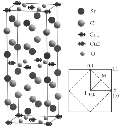
FP-LAPW 10 method treats all electrons without the shape approximations for the potential and charge density. The Perdew-Wang’s exchange-correlation energies are used in the local density approximation (LDA) 16 . In our calculation we have taken the crystal and magnetic structures of the Sr2CuO2Cl2 from Ref. [17]. As shown in Fig. 1, in the antiferromagnetic phase, the unit cell is doubled while the first Brillouin zone (BZ) shrinks to half. The radii of the atomic spheres are taken as 2.0 a.u. for Cu, Cl, and Sr and 1.6 a.u. for O, respectively. And the cutoff of the plane-wave basis is set to =7.0 (the is the plane-wave cut-off, and the is the smallest radius for all atomic sphere radii.). Thus, the resulting number of the plane waves used in our calculation is about 4950 plus 190 local orbitals. Self-consistent calculations are performed with 200 k-points in the first BZ by the tetrahedron method. For checking the numerical convergence, we increase k-points to 500 and find that the difference between the two converged total energies is about 0.02 mRy. In order to include the strong correlation effect of the Cu electrons, we use the LSDA+ approach 18 with =6.0 eV and =125 meV. And the case of =7.5 eV is also calculated for comparison. Here the values are taken from Ref. [8], [19] and [20]. Convergence is assumed when the difference between the input and output charge densities is less than 0.0001 e/(a.u)3 and the difference of total energies in the last two iterations is less than 0.0001 Ry.
Optical responses are calculated within the electric-dipole approximation. The imaginary part of the dielectric function can be expressed by
where and represent the conduction and valence bands, respectively, and , are the eigenstates obtained from the FP-LAPW calculations. p is the momentum operator, is the external electric field vector, and is the frequency of incident photons. We still use 200 sampling k-points in the irreducible wedge and the linear tetrahedron scheme improved by Blöchl et al. 21 for the BZ integrations. Using Kramers-Krönig (K-K) transformation, we can get the real part of the dielectric function, and further calculate the absorption spectrum of the Sr2CuO2Cl2.
III RESULTS AND DISCUSSION
The calculated electronic structures for the AFM Sr2CuO2Cl2 with =6.0 eV are plotted in Fig. 2, 3 and 4. From Fig. 2, it is seen that there is an indirect band gap of about 1.2 eV with the top of the valence band at M(/2, /2) point and the bottom of conduction band at X(, 0) point, which is smaller than the experimental value of 1.9 eV 8 , but much closer to it than the value of 0.84 eV when = 5 eV in Ref. [8]. If a larger =7.5 eV is selected and other parameters are unchanged, an indirect gap of 1.68 eV is obtained, which is very close to the value of 1.63 eV obtained by the LCAO method 8 . The energy dispersion relation agrees very well with the results in Ref. [1] and [2]. But, along the direction from X(, 0) to (0, 0) it is better than that obtained from the model calculation 1 . The energy dispersion of the top-most valence band along (0, 0) to M(/2, /2) reaches to about 0.45 eV, larger than the experimental value of 28060 meV 1 . But calculation with =7.5 eV shows that a larger will suppress the dispersion to 0.32 eV, which is much closer to the experimental value. Anti-ferromagnetic order of Sr2CuO2Cl2 can be clearly seen from Fig. 3(a) and 3(b). The total spin is zero because both of Cu1 and Cu2 have anti-parallel spin moments of about 0.59 per atom, which is also bigger than the experimental value 0.34 17 . It is found that the larger of 7.5 eV will increase the spin moment of Cu atom to 0.63 per atom.
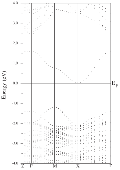


Although the hybridization of O 2p and Cu between -3 and -1.2 eV can be very clearly seen in Fig. 3(b) and 3(c), it is still obvious that the topmost valence band is mostly composed of the O 2p orbital, and a careful analysis shows that near the top of the valence band the O 2p component is about 62.8%. Oppositely it is seen from Fig. 4(a) that the Cu occupies more of the lowest conduction band with its component being about 69.4%. In the case of =7.5 eV, the O 2p component increases to 65.6% at the top of the valence band and Cu occupies more to 70.6% of the lowest conduction band, which indicates that Sr2CuO2Cl2 is a charge transfer insulator. Thus the transition from O 2p to Cu orbitals will dominate the absorption edge. The Cl 3p orbital hybridizes with Cu 3d orbital in the range of from -5 to -3 eV, mostly with Cu and orbitals (see Fig. 3(d), Fig. 4 (b) and (d)), all which are in the plane perpendicular to the Cu-O plane. The hybridization between Cl and Cu is less than that of Cu and O because O 2p orbitals extends more than Cl 3p, and so hybridizes more with Cu 3d orbitals.

Study of optical property can give more informations on the electronic structures. In Fig. 5, absorption spectrum calculated with =6.0 eV are presented. Although =7.5 eV gives the similar spectrum shapes, but all the peaks would shift to higher energy by about 0.4 eV. So, we prefer to take =6.0 eV as an example in the following discussion. Comparing it with the experimental data given by R. Lövenich et.al. 13 and Moskvin et.al. 15 , we find that they match very well near the charge transfer gap of about 2eV, corresponding to electrons transferred from O 2p to Cu 3d orbitals, which can be clearly seen from the band structure in Fig. 2 along the path from X(, 0) to M(/2, /2). Around 2.5 eV, there is one lower peak in both our calculation and Ref. [15], which was deemed by Moskvin et.al. 15 as the other part of the double-peak structure of the lowest excitation. The third strong and broad peak appears at about 3.5 eV. According to the idea of Pothuizen et al. 22 , a nonbonding band (NBB), mostly O 2pπ orbitals, lies at about 1.5 eV below the Zhang-Rice band (ZRB), so the energy needed to transfer an electron from NBB to Cu 3d is about 3.5 eV, which is also shown by Moskvin et al. in their experimental observations. Again, the broad peak around 4.6 eV appears both in our fist-principles result and their measurements. Since the Cu occupies the lowest part of the conduction band from Fermi level to about 1.5 eV, and Cl dominates the most states between -4.5 and -2.5 eV, the quite broad peak around 4.6 eV can be ascribed to the hopping of electrons from Cl orbitals to Cu orbitals, which can be clearly seen from Fig. 3 (b), (d) and Fig. 4 (a). Usually, the CuO4 model calculation on the Sr2CuO2Cl2 has just neglected the Cl effect by replacing the Cl atom by the O atom, while here we have shown the contribution of Cl atoms to the optical properties of the Sr2CuO2Cl2.
Finally, we want to emphasize that correct choice of value is critical for the LSDA+ calculation. One criterion is whether the chosen value can give a reasonable physical result in consistent with the experimental observation. Combining our obtained results with that in Ref. [8] for =5.0 eV, we can see that =6.0 and 7.5 eV are both physically reasonable although the former has been selected for the main discussion on Sr2CuO2Cl2’s optical properties. And it is clear that larger influences Cu orbital more than O , and causes a wider gap, less band dispersion and a bigger magnetic moment on Cu. Also, larger shifts the absorption edge to higher energy.
IV Conclusion
In summary, we have given a more detailed first-principle calculations on the band structure and linear optical properties of the AFM Sr2CuO2Cl2 by using the LSDA+ approach in the FP-LAPW formalism. The obtained results indicate that it is a charge-transfer insulator with an indirect gap of about 1.2 eV, which is less than the experimental value. The vs. k relationship agrees very well to the ARPES observations. Also, we have found that our calculated linear optical susceptibility is well consistent with the experimental data not only around the charge-transfer gap, but also in the higher energy range.
Acknowledgements.
The authors thank support to this work from a Grant for State Key Program of China through Grant No. 1998061407. In addition, H. M. Weng thanks a valuable discussion with Dr. Meichun Qian about the FP-LAPW calculations. Our LSDA+ calculation has been done on the SGI origin 2000 Computer.References
- (1) B. O. Wells, Z. X. Shen, A. Matsuura, D. M. King, M. A. Kastner, M. Greven,and R. J. Birgeneau, Phys. Rev. Lett. 74, 964 (1995).
- (2) C. Kim, P. J. White, Z. X. Shen, T. Tohyama, Y. Shibata, S. Maekawa, B. O. Wells, Y. J. Kim, R. J. Birgeneau, and M. A. Kastner, Phys. Rev. Lett.80, 4245 (1998).
- (3) B. Kyung and Richard A. Ferrell, Phys. Rev. B 54, 10125 (1996).
- (4) T. Xiang and J. M. Wheatley, Phys. Rev. B 54, R12653 (1996).
- (5) V. I. Belinicher, A. L. Chernyshev and V. A. Shubin, Phys. Rev. B 54, 14914 (1996).
- (6) T. K. Lee and C. T. Shih, Phys. Rev. B 55, 5983 (1997).
- (7) R. Eder, Y. Ohta and G. A. Sawatzky, Phys. Rev. B 55, R3414 (1997).
- (8) Hua Wu, Qin-qi Zheng, H. Q. Lin, J. Appl. Phys. 87, 4897 (2000); H. Rosner, M. Johannes, and S. L. Drechsler, J. Appl. Phys. 90, 4880(2001); Hua Wu and Qing-qi Zheng, J. Appl. Phys. 90, 4882 (2001).
- (9) D. L. Novikov, A. J. Freeman, J. D. Jorgensen, Phys. Rev. B 51,6675 (1995).
- (10) P. Blaha, K. Schwarz, G. K. H. Madsen, D. Kvasnicka and J. Luitz, WIEN2k, An Augmented Plane Wave + Local Orbitals Program for Calculating Crystal Properties (Karlheinz Schwarz, Techn. Universität Wien, Austria), 2001. ISBN 3-9501031-1-2.
- (11) M. A. Kastner, R. J. Birgeneau, G. Shirane and Y. Endoh, Rev. Mod. Phys. 70, 897 (1998), and references in it.
- (12) H. S. Choi, Y. S. Lee, T. W. Noh, E. J. Choi, Yunkyu Bang, Y. J. Kim, Phys. Rev. B 60, 4646 (1999).
- (13) R. Löenich, A. B. Schumacher, J. S. Dodge, D. S. Chemla and L. L. Miller, Phys. Rev. B 63, 235104 (2001).
- (14) A. B. Schumacher, J. S. Dodge, M. A. Carnahan,R. A. Kaindl and D. S. Chemla, Phys. Rev. Lett. 87, 127006 (2001)
- (15) A. S. Moskvin, R. Neudert, M. Knupfer, J. Fink and R. Hayn, Phys. Rev. B 65, 180512(R) (2002)
- (16) J. P. Perdew and Y. Wang, Phys. Rev. B 45, 13244 (1992).
- (17) D. Vaknin, S. K. Sinha, C. Stassis, L. L. Miller, D. C. Johnston, Phys. Rev. B 41, 1926 (1990).
- (18) V. I. Anisimov, I. V. Solovyev, M. A. Korotin, M. T. Czyzyk, and G. A. Sawatzky, Phys. Rev. B 48, 16929 (1993).
- (19) A. Yareskoa, R. Haynb, A. Perlovc, H. Rosnerd and P. Thalmeier, Physica B 312-313, 619 (2002)
- (20) M. Greven, R. J. Birgeneau, Y. Endoh, M. A. Kastner, B. Keimer, M. Matsuda, G. Shirane, T. R. Thurston, Phys. Rev. Lett. 72, 1096 (1994).
- (21) Peter E. Blöchl, O. Jepsen, O. K. Andersen, Phys. Rev. B 49, 16223 (1994).
- (22) J. J. M. Pothuizen, R. Eder, N. T. Hien, M. Matoba, A. A. Menovsky, G. A. Sawatzky, Phys. Rev. Lett. 78, 717 (1997)