Kinetic magnetoelectric effect in a 2D semiconductor strip due to boundary-confinement induced spin-orbit coupling
Abstract
In a thin strip of a two-dimensional semiconductor electronic system, spin-orbit coupling may be induced near both edges of the strip due to the substantial spatial variation of the confining potential in the boundary regions. In this paper we show that, in the presence of boundary-confinement induced spin-orbit coupling, a longitudinal charge current circulating through a 2D semiconductor strip may cause strong non-equilibrium spin accumulation near both edges of the strip. The spins will be polarized along the normal of the 2DEG plane but in opposite directions at both edges of the strip. This phenomenon is essentially a kinetic magnetoelectric effect from the theoretical points of view, but it manifests in a very similar form as was conceived in a spin Hall effect.
pacs:
72.25.-b, 75.47.-mI Introduction
There has recently been much interest in a fascinating topic in the research community, namely spin Hall effect ( SHE ). SHE is such a phenomenon that a transverse spin current is generated when a longitudinal charge current circulates through a sample, and if the sample has a thin strip geometry, the transverse spin current will cause non-equilibrium spin accumulation at both edges of the sampleHirsch1999 ; MurakamiScience2003 ; SinovaPRL2004 . Such a phenomenon would be much useful in the context of semiconductor spin-based electronics ( spintronics ) because it might provide an effective way for generating spin currents and/or non-equilibrium spin density in a nonmagnetic semiconductors without use of ferromagnetic metals or ferromagnetic semiconductors, a principal challenge in semiconductor spintronicsDassarma2004 ; semibook2002 . From the theoretical points of view, such a phenomenon can arise from either intrinsic spin-orbit ( SO ) coupling ( i.e., spin-orbit splitting of the band structure )MurakamiScience2003 ; SinovaPRL2004 or extrinsic SO coupling ( i.e., spin-orbit dependent impurity scatterings )Hirsch1999 ; DP71 in a semiconducting material, and correspondingly, the phenomena due to intrinsic SO coupling was termed intrinsic spin Hall effect and the phenomena due to spin-orbit dependent impurity scatterings termed extrinsic spin Hall effect. From the standpoint of spintronic applications, intrinsic SHE are more attractive since it is an intrinsic property of a semiconducting material and does not rely on spin-orbit dependent impurity scatteringsMurakamiScience2003 ; SinovaPRL2004 . Recently two experiments were reported on the observation of SHE. One is on -doped bulk GaAs by Kato et al.KatoScience2004 and the other is on two-dimensional -doped GaAs by Wunderlich et al.WunderlichPRL2005 . The phenomenon observed in two-dimensional -doped GaAs by Wunderlich et al. was believed to be an intrinsic spin Hall effect since the edge spin accumulation measured in a thin strip of such a system is insensitive to impurity scatterings in the weak impurity scattering regimeWunderlichPRL2005 , an important feature of intrinsic spin Hall effectMurakamiScience2003 ; SinovaPRL2004 . In contrast, the phenomenon observed in -doped bulk GaAs by Kato et al. was believed to have an extrinsic origin ( i.e., due to spin-orbit dependent impurity scatterings ) since the edge spin accumulation measured in a thin strip of such a system is several order of magnitude smaller compared with the theoretical predictions of Refs.[2-3]. Although substantial progresses have been achieved on the detection of spin Hall effect, it should be noted that from the theoretical points of view there are still intensive debates on whether intrinsic spin Hall effect does can survive in a spin-orbit coupled system. For example, several recent theoretical works have argued that, except for the ballistic transport limit, intrinsic spin Hall effect cannot survive in a diffusive two-dimensional electron gas with Rashba spin-orbit coupling even in the weak impurity scattering limitInouePRB2004 ; MishchenkoPRL2004 ; RashbaPRB2003 ; Raim05 ; Dim05 ; Szhang05 ; Kha06 . As to the physical understanding of the recent experimental resultsKatoScience2004 ; WunderlichPRL2005 , some significant controversies also exist which needs further clarifications. For details please refer to Refs.[16-25].
In this paper, we investigate theoretically another kind of electric-field driven edge spin-accumulation which might occur in a thin strip of a two-dimensional electronic ( electron or hole ) system. From the theoretical points of view, this phenomenon is essentially a kinetic magnetoelectric effectEdelstein due to boundary-confinement induced spin-orbit coupling ( which will be called edge SO coupling below ). But very interestingly, it would manifest in a very similar manner as was conceived in an spin Hall effect. For example, the electric-field driven edge spin accumulation in a thin 2DEG strip due to this phenomenon will be polarized perpendicular to the 2DEG plane but along opposite directions at both edges of the strip; and in the weak impurity scattering regime ( below a certain disorder strength ) the edge spin accumulation will not decrease as the disorder strength increases, thus it can survive even in the diffusive transport regime. These features are very similar to the recently discovered spin Hall effect, but the mechanisms involved in this phenomenon are very different from that of the usual spin Hall effect from the theoretical points of view. The results obtained in the present paper might provide some new implications to the proper physical understanding of the recent experimental resultsKatoScience2004 ; WunderlichPRL2005 .
The paper is organized as following: in section II an edge SO coupling model describing the boundary-confinement induced SO coupling in a thin 2DEG strip will be introduced and some details of the theoretical formalism used in the paper will be briefly explained, and in section III some numerical results will be presented and discussed.
II Model and Theoretical Formulation
The system considered in the present paper consists of a thin 2DEG strip connected to two ideal leads, as was shown in Fig.1(a). According to the theory of the relativistic quantum mechanics, if the movement of an electron is confined by a spatially non-uniform potential, the spin and orbital degree of freedom of the electron will be coupled togetherMerz . The longitudinal direction of the strip will be defined as the direction and the normal of the 2DEG plane defined as the direction. For the sake of simplification, we assume that the confining potential is spatially uniform along the longitudinal direction of the strip, i.e., the spatial variation of the confining potential occurs only in the transverse direction of the strip ( defined as the direction ). Under this assumption, the SO coupling due to the transverse spatial variation of the confining potential will take the following formMerz ; wink ,
| (1) |
where are the usual Pauli matrices, is the wave vector of electrons, denotes the usual gradient operator and is the transverse confining potential, which depends only on the coordinates. From the effective Hamiltonian (1) one can see that, for an electron moving along the ( or ) direction, the SO coupling will tend to force the electron spin to align along the ( or ) direction, depending on the sign of . In the absence of external electric field, the numbers of electrons moving along the and directions are equal and no net spin density can be resulted. However, if an external electric field is applied in the longitudinal direction of the strip, the numbers of electrons moving to direction will be larger than the number of electrons moving to the direction, and hence a net spin density polarized along the or direction might be resulted from the SO coupling. Such an effect was dubbed the kinetic magnetoelectric effect in the literatureEdelstein .

For a 2DEG strip, if the strip width is much larger than the lattice constant, one can further assume that the confining potential varies substantially only in a narrow boundary region as was shown in Fig.1(b). ( We assume that the two boundaries of the srip are located at ). Then the SO coupling exists only near both edges of the strip, and due to the symmetry of the confining potential, the SO coupling coefficient ( proportional to ) has opposite signs at both edges of the strip, as was shown in Fig.1(c). Thus, the edge SO coupling model described by the effective Hamiltonian (1) implies that the electric-field driven spin accumulation will be polarized along opposite directions ( normal to the 2DEG plane ) at both edges of the strip, similar to a spin Hall effect. This will be confirmed by detailed numerical calculations below. In order to make a comparison with the widely studied intrinsic spin Hall effect in a Rashba two-dimensional electron gas, we can also include a Rashba SO coupling in our edge SO coupling model. Then the total Hamiltonian of the 2DEG strip will be
| (2) |
where the second term is the Rashba SO coupling ( which arises from the inversion asymmetry of the trapping well along the normal of the 2DEG plane ) and the Rashba SO coupling constant. ( is a unit vector along the normal of the 2DEG plane ). A direct use of the Hamiltonian (2) is not convenient if one wants to take into account the effects of impurity scatterings properly, which are very important in the diffusive transport regime. So in our calculations we will transform the Hamiltonian (2) into a discrete form. The discrete version of the effective Hamiltonian for the total system ( including both the leads and the 2DEG strip ) will read:
| (3) | |||||
Here is the hopping matrix element between two nearest-neighbour sites and the lattice constant in the 2DEG strip. is the annihilation operators of electrons at the lattice site in the strip. is the annihilation operator of electrons with spin at the lattice site in the lead ( ). stands for a nearest-neighbor pair of lattice sites across the interfaces between the 2DEG strip and the leads. is the on-site energy in the 2DEG strip. In a clean system without disorder, one usually sets to be zero. is the Rashba SO coupling coefficient in the 2DEG strip, which is assumed to be site-independent. The last term in Eq. (3) stands for the boundary-confinement induced SO coupling and is the coupling coefficient, which is site-dependent. The site-dependence of will be determined by the actual form of the transverse confining potential in the 2DEG strip. In our calculations we assume a parabolic confining potential near both edges of the strip, as was shown in Fig.1(b). In such cases, the site-dependence of the edge SO coupling coefficient can be expressed as
| (4) |
where is the width of the strip (in units of lattice constant), is the width of the narrow boundary regions in which the edge SO coupling exists, and is the minimum value of the site-dependent edge SO coupling coefficient. The sign is different for the two edges, as shown in Fig.1(c).
Our calculations will be based on the Landauer-Buttiker formula. To this end, we first consider the transmission and reflection of an electron incident from a lead. The real space wave function of an incident electron with spin will be denoted as , where denotes the ’th transverse mode with spin index in the lead and the longitudinal wave vector. We adopt the local coordinate scheme for all leads. In the local coordinate scheme, the longitudinal coordinate in the lead will take the integer numbers …, away from the 2DEG interface and the transverse coordinate take the value of . The longitudinal wave vector satisfys the relation , where is the eigen-energy of the ’th transverse mode in the lead and the energy of the incident electron. Including both the incident and reflected waves, the total wave function in the lead has the the following general form:
| (5) | |||||
where stands for the scattering amplitude from the () mode in the lead to the () mode in the lead . To obtain the scattering amplitudes from the Schrödinger equation ( which has now a lattice form and hence there is a separate equation for each lattice site and spin index ), we must solve the wave function in the 2DEG strip simultaneously. As dealing with usual scattering problems in quantum mechanics, we use boundary conditions to determine the scattering amplitudes . In the lattice formalism, the wave functions in the entire 2DEG strip and in the first row of the leads ( i.e., ) will be involved in the boundary conditions, which will be determined from the Schrödinger equation. Because Eq.(5) is a linear combination of all out-going modes with the same energy , the Schrödinger equation is satisfied automatically in the lead , except for the lattice sites in the first row ( i.e., ) of the lead which are connected directly to the 2DEG strip. The wave function in the first row of a lead ( which are determined by the scattering amplitudes ) must be solved simultaneously with the wave function in the 2DEG strip. To simplify the notations, the wave function in the 2DEG strip will be defined as a column vector whose dimension is ( is the total number of lattice sites in the 2DEG strip ). The scattering amplitudes will be arranged as a column vector whose dimension is ( is the total number of lattice sites in the first row of the leads ). From the Schrödinger equation for the 2DEG strip and for the first row of a lead, one can show that the boundary conditions at the interface between a lead and the 2DEG strip can be expressed as the following forms:
| (6) |
where and are two square matrices with a dimension of and , respectively; and are two rectangular matrices describing the hopping interaction between the leads and the 2DEG strip, whose matrix elements will depend on the actual form of the geometry of the system. The vectors and describe the contributions from the incident waves. The details of these matrices and vectors will be given elsewhereJiang2 .
After obtaining all scattering amplitudes from the boundary conditions, we can calculate the charge current in each lead through the Landauer-Buttiker formula, , where is the voltage applied in the lead and is the chemical potential in the lead , are the transmission probabilities defined by and is the velocity for the ’th mode in the lead . The spin current in each lead can be calculated similarly, . With the wave function in the 2DEG strip at hand, the non-equilibrium spin density in the 2DEG strip can also be calculated readily by taking proper ensemble average, and the results can be expressed as
| (7) |
where denotes the spin density at the lattice site in the 2DEG strip.
III Results and Discussions
In our calculations we will take the typical values of the electron effective mass and the lattice constant NIttaPRL1997 . The chemical potentials in the leads will be set by fixing the longitudinal charge current density to the experimental value ( ) as reported in Ref.[8]. The Fermi energy of the 2DEG strip will be set to throughout the calculations.
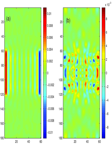
In Fig.2(a) we show the typical pattern of the spatial distribution of the electric-field induced nonequilibrium spin density in the 2DEG strip obtained based on the edge SO coupling model. ( Other components of the spin density is zero in the case of the edge SO coupling model, which were not shown in the figure ). We have used lattice sites in total ( including both the leads and the 2DEG strip ) in the calculations and the 2DEG strip contains lattice sites. From Fig.2(a) one can see that, the spatial distribution of the electric-field induced nonequilibrium spin density in the 2DEG strip obtained based on the edge SO coupling model manifests in a very similar form as was conceived in a spin Hall effectKatoScience2004 ; WunderlichPRL2005 , i.e., the spins are polarized perpendicular to the 2DEG plane but along opposite directions on both edge of the strip and the spin density has two opposite extrema near both edges. By fixing the longitudinal charge current density to the experimental value ( ) as reported in Ref.[8] and setting the edge SO coupling coefficient to , we found that the spin polarization in the 2DEG strip obtained based on the edge SO coupling model ( ) has roughly the same order of magnitude as the corresponding experimental values reported in Ref.[8]. To make a comparison with the widely studied Rashba SO coupling modelNikolicPRL2005 , in Fig.2(b) we have also plotted the spatial distribution of the electric-field induced nonequilibrium spin density in the 2DEG strip obtained based on the usual Rashba SO coupling model. From Fig.2(a) and 2(b) one can see that the typical patterns of the spatial distribution of the electric-field induced nonequilibrium spin density are very similar in both cases. But it should be pointed out that, in the case of our edge SO coupling model, only the component of the spin density is non zero. In contrast, for the case of the usual Rashba model, all three components of the spin density are nonzero. ( In Fig.2(b) we have plotted only the spatial distribution of the component of the spin density for comparison ). Another slight difference that can be seen from Fig.2(a) and 2(b) is that, the transverse spatial distribution of the spin density has a very regularly striped pattern in the case of the edge SO coupling model, but for the case of the usual Rashba model, the spin-density pattern is not much regularly striped. This slight difference arises from the fact that, in the case of our edge SO coupling model, the SO coupling exists only in a narrow boundary region near both edge of the 2DEG strip ( see the illustration shown in Fig.1(b-c) ) and was assumed to be uniform along the longitudinal direction of the strip. These assumptions lead to a regularly striped spin-density pattern as shown in Fig.2(a). For the case of the usual Rashba model, the SO coupling exists in entire the strip ( i.e., the SO coupling coefficient is nonzero everywhere in the strip ), thus the spin-density pattern in the strip is not much regularly striped.
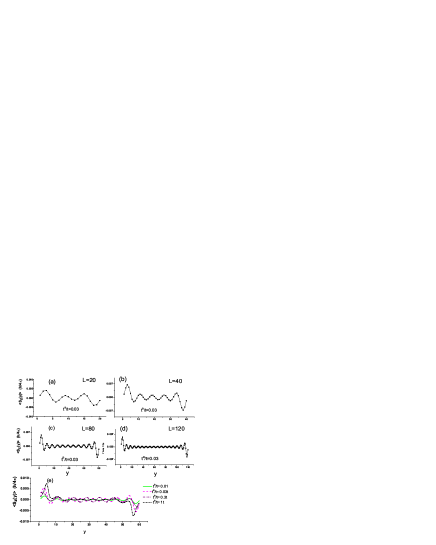
Next, we study the dependence of the edge spin accumulation on the strip width and the SO coupling strength in the case of the edge SO coupling model. Because the spatial distribution of the spin density has a regularly striped pattern along the longitudinal direction, we can use an averaged value of , defined by , as a measure of the spin accumulation. In Fig.3(a-d) we plot the profiles of the transverse spatial distribution of the spin accumulation obtained in several different cases with different lattice sizes. From these figures one can see that, oscillates inside the strip and has opposite signs on both edges of the strip, and the magnitude of the spin density will reach a maximum value ( denoted as below ) near both edges of the strip. As the strip width increases, the transverse spatial distribution of the spin accumulation become sharper and sharper near both edges of the strip and the oscillations of the amplitude of the spin density inside the strip tend to be smeared, i.e., the spin accumulation will be localized near both edges of the strip if the strip width is much larger than the lattice constant. From these figures one can also note that, the order of the magnitude of the spin density near both edges of the strip remains unchanged as the strip width increases, suggesting that the electric-field induced edge spin accumulation due to boundary-confinement induced edge SO coupling can survive even in the diffusive transport regime, similar to the phenomenon reported in Ref.[8]. ( For a 2D semiconductor strip with Rashba spin-orbit coupling, it was generally believed that the intrinsic spin Hall effect can not survive in the diffusive transport regimeInouePRB2004 ; MishchenkoPRL2004 ; RashbaPRB2003 ; Raim05 ; Dim05 ; Szhang05 ; Kha06 ). The dependence of the transverse spatial distribution of the spin density on the edge SO coupling strength was shown in Fig.3(e), from which one can see that the profiles of the transverse spatial distribution of the spin density do not change substantially as the edge SO coupling strength varies.
Finally, we discuss the effects of random impurity scatterings on the electric-field induced nonequilibrium spin density in the case of the edge SO coupling model. To include properly the effects of random impurity scatterings, we assume that the on-site energy in the 2DEG strip are randomly but uniformly distributed in an energy region , where is the amplitude of the on-site energy fluctuations, which characterizes the disorder strengthLShengPRL2005 ; NikolicPRB2005 . We will calculate the spin density for a number of random impurity configurations and then do impurity average. In Fig.4(a-b) we show the relation between the edge spin accumulation and the disorder strength in both cases of (a) the edge SO coupling model and (b) the usual Rashba model, respectively. We have done impurity average over 10000 random impurity configurations for each case. From Fig.4(a) one can see that, for the case of the edge SO coupling model, the edge spin accumulation does not decrease ( or may even increase ) as the disorder strength increases in the weak impurity scattering regime ( i.e., below a certain disorder strength ) and for a fixed longitudinal change current density ( ), similar to the intrinsic spin Hall effect observed by Wunderlich et al.WunderlichPRL2005 . In contrast, for the case of the Rashba model, the edge spin accumulation decreases monotonously as the disorder strength increases even in the weak impurity scattering limit, which can be seen clearly from Fig.4(b).
The different behaviors in these two models can be understood qualitatively as following. For the edge SO coupling model, the SO coupling exists only in a narrow boundary region near both edges of the strip ( see the illustration shown in Fig.1(b-c) ). The electric-field induced nonequilibrium spin density in this model is due to the kinetic magnetoelectric effect but not due to the flow of a transverse spin Hall current, thus only those scattering events occurred near both edges of the strip will affect substantially the spin density. In contrast, for the case of the Rashba model, the electric-field induced nonequilibrium spin density is due to the flow of a transverse spin Hall currentNikolicPRL2005 , which will be damped significantly by all random impurity scattering events occurred in entire the strip and hence the edge spin accumulation will be decreased substantially with increasing disorder strength even in the weak impurity scattering limit. Of course, because localization effects will become important in the presence of strong impurity scatterings, the electric-field induced nonequilibrium spin density in the case of the edge SO coupling model will also be decreased substantially in the presence of strong impurity scatterings, which can be seen clearly from Fig.4(a).
In summary, we have presented a microscopic model calculation for the kinetic magnetoelectric effect in a thin strip of a two-dimensional electronic system due to boundary-confinement induced edge SO coupling. We have shown that this effect can manifest in a very similar form as was conceived in a spin Hall effectKatoScience2004 ; WunderlichPRL2005 , and some important features of this effect are similar to the intrinsic spin Hall effect observed recently in thin strips of two-dimensional p-doped semiconductorsWunderlichPRL2005 . The results obtained in the present paper may provide some new implications to the proper physical understanding of the recent experimental results.
Acknowledgements.
Y. J. Jiang was supported by Natural Science Fundation of Zhejiang province ( Grant No.Y605167 ). L. B. Hu was supported by the National Science Foundation of China ( Grant No.10474022 ) and the Natural Science Foundation of Guangdong province ( No.05200534 ).References
- (1) J. E. Hirsch, Phys. Rev. Lett. 83,1834(1999); S. Zhang, Phys. Rev. Lett. 85, 393(2000).
- (2) S. Murakami, N. Nagaosa, and S. C. Zhang, Science 301, 1348(2003).
- (3) J. Sinova, D. Culcer, Q. Niu, N. A. Sinitsyn, T. Jungwirth, and A. H. MacDonald, Phys. Rev. Lett. 92, 126603(2004).
- (4) I. Zutic, J. Fabian, and S. Sarma, Rev. Mod. Phys 76, 323(2004).
- (5) D. Awschalom, D. Loss, and N. Samarth, Semiconductor Spintronics and Quantum Computation ( Springer, Berlin, 2002).
- (6) I. Dyakonov and V. I. Perel, Sov. Phys. JETP 33, 467(1971).
- (7) Y. K. Kato, R. C. Myers, A. C. Gossard, and D. D. Awschalom, Science 306, 5703(2004).
- (8) J. Wunderlich, B. Kaestner, J. Sinova, and T. Jungwirth, Phys. Rev. Lett. 94, 047204(2005).
- (9) J. Inoue, G. E. W. Bauer, and L. W. Molenkamp, Phys. Rev. B70, 041303(R)(2004).
- (10) E. G. Mishchenko, A. V. Shytov, and B. I. Halperin, Phys. Rev. Lett. 93, 226602(2004).
- (11) E. I. Rashba, Phys. Rev. B 68, (R)241315(2003); ibid.70, (R)201309(R)(2004).
- (12) R. Raimondi and P. Schwab, Phys. Rev. B 71, 033311 (2005).
- (13) O. V. Dimitrova, Phys. Rev. B 71, 245327 (2005).
- (14) S. Zhang and Z. Yang, Phys. Rev. Lett. 94, 066602(2005).
- (15) A. Khaetskii, Phys. Rev. Lett. 96, 056602(2006).
- (16) B. K. Nikolic, S. Souma, L. P. Zarbo and J. Sinova, Phys. Rev. Lett 95, 046601(2005).
- (17) B. K. Nikolic, L. P. Zarbo and S. Souma, Phys. Rev. B 72, 075361(2005); ibid.73, 075303(2006).
- (18) L. Sheng, D. N. Sheng, and C. S. Ting, Phys. Rev. Lett. 94, 016602(2005); Q. Wang, L. Sheng, and C. S. Ting, cond-mat/0505576.
- (19) A. G. Malshukov, L. Y. Wang, C. S. Chu, and K. A. Chao, Phys. Rev. Lett. 95, 146601(2005).
- (20) H. A. Engel, B. I. Halperin, and E. I. Rashba, Phys. Rev. Lett. 95, 166605 (2005).
- (21) W. K. Tse and S. Das Sarma, Phys. Rev. Lett. 96, 056601 (2006).
- (22) A. Reynoso, G. Usaj, and C. A. Balseiro, cond-mat/0511750.
- (23) V. M. Galitski, A. A. Burkov, S. Das Sarma, cond-mat/0601677.
- (24) X. H. Ma, L. B. Hu, R. B. Tao, and S. -Q. Shen, Phys. Rev. B 70, 195343(2004); L. B. Hu, J. Gao, and S. -Q. Shen, Phys. Rev. B 70, 235323(2004).
- (25) Y. J. Jiang, cond-mat/0510664.
- (26) V.M. Edelstein, Solid State Commun. 73, 233 (1990).
- (27) E. Merzbacher, Quantum mechanics ( John Wiley & Sons Inc., 1998 ).
- (28) R.Winkler, Spin-Orbit Coupling Effects in Two Dimensional Electron and Hole Systems (Springer,Berlin, 2003).
- (29) Y. J. Jiang and L. B. Hu ( unpublished ).
- (30) J. Nitta, T. Akasaki, and H. Takayanagi, Phys. Rev. Lett 78, 1335(1997).