Single-crystalline nanopillars for spin-transfer measurements
Abstract
We report on current-induced magnetization switching (CIMS) in single- crystalline nanopillars. Fe(14 nm)/Cr(0.9 nm)/Fe(10 nm)/Ag(6 nm)/Fe(2 nm) multilayers are deposited by molecular-beam epitaxy. The central Fe layer is coupled to the thick one by interlayer exchange coupling over Cr. The topmost Fe layer is decoupled (free layer). Nanopillars with 150 nm diameter are prepared by optical and e-beam lithography. The opposite spin scattering asymmetries of Fe/Cr and Fe/Ag interfaces enable us to observe CIMS at small magnetic fields and opposite current polarity in a single device. At high magnetic fields, step-like resistance changes are measured at positive currents and are attributed to current-driven magnetic excitations.
pacs:
75.47.-m, 72.25.Ba, 75.60.JkIn a magnetic multilayer containing two ferromagnetic layers and a nonmagnetic spacer (FM2/NM/FM1), an electric current flowing perpendicularly to the layers (CPP) gets spin-polarized by the FM layers, leading to a giant magnetoresistance (GMR)baibich88 ; binasch89 . Thus, spin currents can sense the magnetization state of the magnetic system. Slonczewski slonczewski96 and Berger berger96 first predicted that spin currents of appropriate strength can also directly influence the magnetizations without applying an external magnetic field. Electrons flowing from FM2 to FM1 are first polarized by FM2 and then repolarized at the interface NM/FM1, where the transverse component of the spin current is absorbed and acts as a torque on the magnetic moment of FM1 stiles02 . By reversing the current direction, the spin current reflected from FM2 is repolarized at the NM/FM1 interface leading to a reversed torque. Therefore, FM1 can be switched from the parallel to the antiparallel configuration with respect to FM2 back and forth by repeatedly reversing the current polarity, as long as remains fixed. This pinning can be achieved by different FM layer thicknesses albert00 ; grollier01 ; urazhdin03 , by the exchange bias effect krivorotov05 , or by making use of interlayer exchange coupling, as in our case.
In order to achieve large spin-torque effects a high spin polarization of the current is needed. Thus, the present work is motivated by two publications of Stiles and Penn stiles00 and Stiles and Zangwill stiles02 , in which the authors predict high spin polarization for single-crystalline Fe/Ag interfaces. Single-crystalline layered structures can also serve as model systems for comparison with theory due to the well known structure, the small amount of defects, and the homogeneous magnetic properties when prepared by molecular beam epitaxy (MBE). In particular, single-crystalline Fe(001) layers show well-defined 4-fold in-plane magnetocrystalline anisotropy, which also helps to stabilize the magnetization along two easy axes ([100] and [010]).
First, we deposit the magnetic multilayer. In order to achieve single-crystalline growth we use a standard MBE system. The native oxygen layer of the GaAs(001) substrates () is desorbed by annealing for 60 min at under UHV conditions. We deposit 1 nm Fe and 150 nm Ag at to get a flat buffer system after annealing at for buergler96 . The Ag buffer also act as a bottom electrode for the transport measurements. The following layers are then deposited at room temperature: Fe(14)/Cr(0.9)/Fe(10)/Ag(6)/Fe(2) [thicknesses in nm]. We check the crystalline surface structure after each deposited layer by low-energy electron diffraction (LEED). The spots characteristic of (001) surfaces slightly broaden with increasing total thickness, but still indicate high crystalline quality, even for the final 50 nm Au(001) capping layer. Thicknesses are controlled by quartz crystal monitors. The bottom and central FM layers [Fe(14) and Fe(10)] are coupled by interlayer exchange coupling over the Cr interlayer. Therefore, the central Fe(10) layer is magnetically harder with respect to the top Fe(2) layer.
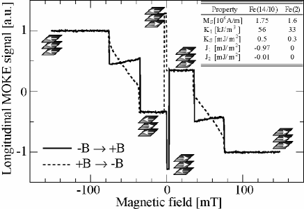
The longitudinal magneto-optical Kerr effect (MOKE) is used to measure the magnetic properties of the samples. In Fig. 1 we present the hysteresis loop with the magnetic field parallel to one of the easy [100]-axes of the Fe layers in the film plane. The saturation field of the system is . For smaller magnetic fields the central Fe(10) layer remagnetizes via a canted state to the fully antiferromagnetic configuration of the trilayer stack below the switching field mT. After reversing the field direction we measure another jump in the signal, which corresponds to the reversal of the topmost nm thick Fe layer at mT. At mT the two coupled Fe layers reverse simultaneously due to their unequal thickness.
By fitting the MOKE measurements and additional Brillouin Light Scattering measurements (BLS) buchmeier03a we extract the magnetic properties of each layer as compiled in the inset of Fig. 1. The saturation magnetization and the crystalline anisotropy have bulk values kittel96 ; wohlfarth80 and indicate the high quality of the layers. The thin Fe(2) layer has reduced and , which can be understood by the reduced thickness or by reduced growth quality. The negligible coupling constants and show that this layer is decoupled. denotes the interface anisotropy.
In order to measure the spin-transfer effects in the CPP-geometry we have developed a combined process of optical and e-beam lithography. First, we define the leads and contact pads of the bottom electrode by using AZ5206 photoresist and ion beam etching (IBE). We then employ HSQ (hydrogen silsesquioxane) as negative e-beam sensitive resist namatsu98 and a Leica EBPG 5HR e-beam writer to define small nanopillars. The resist structures are circular and transferred into the magnetic layers by IBE. The timed etching process is stopped inside the magnetic multilayer. Typical dimensions of the developed resist structures are 100 - 150 nm (measured with an atomic force microscope). Due to redeposition of etched material during IBE gloersen75 , the nanopillars broaden to 150 - 200 nm. The pillars are planarized by spin-coating HSQ. Subsequent e-beam exposure turns HSQ into SiOx, which electrically insulates the pillars namatsu98 . In order to improve the insulation, especially at the side walls of the bottom electrodes, a 50 nm Si3N4 layer is deposited by plasma enhanced chemical vapor deposition (PECVD). We open the top of the nanopillars by IBE and use an optical lift-off process of 300 nm Au for the preparation of the top electrode for the 4-point resistance measurements.
The DC voltage drop of a constant current applied to the junction is measured, and by dividing by we calculate the absolute resistance . The differential resistance is recorded with lock-in technique by mixing a constant current with a small modulated voltage ( and kHz). Typical junction resistances lie in the range between 1 and 3 . The temperature can be controlled with a He flow cryostat between 4 and 300 K.
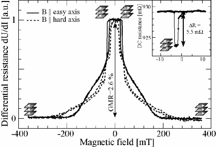
The magnetoresistance loop of a junction without applying a DC bias current is shown in Fig. 2. The solid (dashed) line represents the data with magnetic field along the easy (hard) axis of Fe(001). The curves show a completely different behavior for the two field directions, but are the same along the second pair of easy and hard axes. Thus, the structure is still single-crystalline and exhibits 4-fold magnetocrystalline anisotropy. The saturation field of the structured sample is 190 mT, which is more than twice the saturation field of the extended layers (see Fig. 1). Another difference becomes obvious in the minor loop (inset of Fig. 2), where the absolute resistance is measured with a small DC current of 1 mA. Coming from large positive magnetic field, the resistance drops to a smaller value at small reversed fields between 1 and 3 mT and jumps back to the high resistance state at larger negative fields. On the way back, the resistance stays at the maximum value. The drop on the first half of the cycle does not occur on every measurement. Thus, the patterning has modified the magnetic configuration and the structured Fe(2) nanomagnet is presumably coupled to the rest of the system by dipolar stray fields at the edges or by domain wall coupling. This is a common feature in these devices also seen in Co nanopillars albert00 . Due to this effect, we cannot separate the contributions of both subsystems to the GMR, and therefore cannot gauge the resistance jumps measured under the influence of a large DC current in Fig. 3. The dramatic increase in the saturation field can also be explained by the competition between the interlayer exchange coupling, external, and dipolar fields.
The overall GMR ratio defined as , where is the highest resistance value in the antiferromagnetic configuration and denotes the smallest resistance in the saturated state, amounts to 2.6% at RT and 5.6% at 4 K.
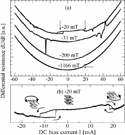
A DC current influences the resistance and, at some critical values, the magnetization state of the junction (Fig. 3). Positive current corresponds to an electron flow from the “free” Fe(2) to the “fixed” Fe(10) layer. We observe a parabolic background which has been measured previously albert00 ; grollier01 ; urazhdin03 ; krivorotov05 and is usually explained by Joule heating of the junction. On top of that, we measure field dependent resistance changes, which can be attributed to spin-torque effects. For instance at -20 mT [Fig. 3(b)], the resistance drops at mA from the high-resistive to an intermediate state. After reducing the current again, the resistance jumps back to the large value. But also at negative bias the resistance changes at mA from large to small. With an estimated junction diameter of nm the corresponding critical current densities are and . As already mentioned in the discussion about the GMR data of Fig. 2 we cannot directly relate the resistance jumps to changes between specific magnetization states.
If we start the measurement in the intermediate resistance state at a field of -31 mT, the canted alignment is the initial state. But at large positive and negative currents (+31.4 and -24.8 mA) we observe strong deviations from the parabolic background that may indicate current-driven high-frequency excitations of the magnetization.
The occurrence of jumps at both polarities of the current at small fields is at first glance surprising, but can be explained by taking into account that both Fe/Cr and Fe/Ag interfaces contribute and have spin scattering asymmetries with opposite signs stiles00 ; alhajdarwish04 . This leads for the Fe/Cr subsystem to inverse current-induced magnetization switching, very similar to inverse GMR geor94-1 ; buch03-2 . Thus, the spin torques for the two subsystems are inverted. For instance, a negative current stabilizes the parallel state for Fe/Ag/Fe and the antiparallel state for Fe/Cr/Fe. At low fields, the central Fe(10) layer points opposite to the external magnetic field (Fig. 1). At positive currents, the spin-transfer torque generated in the Fe/Cr subsystem destabilizes this direction and switches the Fe(10) layer [Fig. 3(b)]. At negative currents, the Fe(2) layer gets unstable by the torque created from the Fe/Ag subsystem, while the Fe/Cr subsystem is even stronger stabilized in the antiparallel state.
At large magnetic fields exceeding the saturation field [e.g., -1166 mT in Fig. 3(a)], the two thick bottom layers [Fe(14) and Fe(10)] are stronger stabilized by the Zeeman energy than the Fe(2) layer, and therefore only one step-like resistance change due to magnetic excitations of Fe(2) at is observed under these conditions.
In conclusion, we have prepared single-crystalline nanopillars by molecular beam epitaxy and a combined process of optical and e-beam lithography. The extended multilayers are characterized by MOKE and compared to CPP-GMR data of the nanopillars, which clearly show the 4-fold magnetocrystalline anisotropy of Fe. The large GMR ratio of up to 5.6% at 4 K reflects the high spin polarization predicted in Refs. stiles00 ; stiles02 . After the patterning process the magnetic properties change so that the “free” Fe(2) layer is now coupled to the rest of the system by dipolar stray fields. Under the influence of a DC current we are able to measure distinct resistance changes, which give clear evidence of spin-torque effects at current densities of about . This value is mostly determined by the sizable dipolar coupling in the nanopillar. At high magnetic fields, step-like resistance changes are measured at positive currents and are attributed to current-driven magnetic excitations. The opposite spin scattering asymmetries of Fe/Cr and Fe/Ag enable us to observe CIMS at small magnetic fields for both subsystems in a single device. The switching at opposite current polarity provides opportunities for optimizing the CIMS behavior and realizing further magnetic excitation dynamics, e.g. by exciting one subsystem at higher current density while simultaneously suppressing excitations of the fixed layer with the torque exerted by the second subsystem.
References
- (1) M. N. Baibich, J. M. Broto, A. Fert, F. Nguyen van Dau, P. Etienne, G. Creuzet, A. Friederich, and J. Chazelas, Phys. Rev. Lett. 61, 2472 (1988).
- (2) G. Binasch, P. Grünberg, F. Saurenbach, and W. Zinn, Phys. Rev. B 39, 4828 (1989).
- (3) J. C. Slonczewski, J. Magn. Magn. Mater. 159, L1 (1996).
- (4) L. Berger, Phys. Rev. B 54, 9353 (1996).
- (5) M. D. Stiles and A. Zangwill, Phys. Rev. B 66, 014407 (2002).
- (6) F. J. Albert, J. A. Katine, and R. A. Buhrman, Appl. Phys. Lett. 77, 3809 (2000).
- (7) J. Grollier, V. Cros, A. Hamzic, J. M. George, H. Jaffrés, A. Fert, G. Faini, J. Ben Yousssef, and H. Legall, Appl. Phys. Lett. 78, 3663 (2001).
- (8) S. Urazhdin, N. O. Birge, W. P. Pratt Jr., and J. Bass, Phys. Rev. Lett. 91, 146803 (2003).
- (9) I. N. Krivorotov, N. C. Emley, J. C. Sankey, S. I. Kiselev, D. C. Ralph, and R. A. Buhrmann, Science 307, 228 (2005).
- (10) M. D. Stiles and D. R. Penn, Phys. Rev. B 61, 3200 (2000).
- (11) D. E. Bürgler, C. M. Schmidt, J. A. Wolf, T. M. Schaub, and H. J. Güntherodt, Surf. Sci. 366, 295 (1996).
- (12) M. Buchmeier, private communication (unpublished).
- (13) M. Buchmeier, B. K. Kuanr, R. R. Gareev, D. E. Bürgler, and P. Grünberg, Phys. Rev. B 67, 184404 (2003).
- (14) C. Kittel, Einführung in die Festkörperphysik, 11. ed. (R. Oldenbourg Verlag, München Wien, 1996).
- (15) Ferromagnetic Materials, edited by E. P. Wohlfarth (North-Holland Publishing Company, Amsterdam New York Oxford, 1980).
- (16) H. Namatsu, T. Yamaguchi, M. Nagase, K. Yamazaki, and K. Kurihara, Microelectron. Eng. 41/42, 331 (1998).
- (17) P. G. Glöersen, J. Vac. Sci. Technol. 12, 28 (1975).
- (18) M. AlHajDarwish, H. Kurt, S. Urazhdin, A. Fert, R. Loloee, W. P. Pratt Jr., and J. Bass, Phys. Rev. Lett. 93, 157203 (2004).
- (19) J. M. George, L. G. Pereira, A. Barthélémy, F. Petroff, L. Steren, J. L. Duvail, A. Fert, R. Loloee, P. Holody, and P. A. Schroeder, Phys. Rev. Lett. 72, 408 (1994).
- (20) M. Buchmeier, R. Schreiber, D.E. Bürgler, and P. Grünberg, Europhys. Lett. 63, 874 (2003).