Interferometric detection of spin-polarized transport in the depletion layer of a metal-GaAs Schottky barrier
Abstract
It is shown that the Kerr rotation of spin-polarized electrons is modulated by the distance of the electrons from the sample surface. Time-resolved Kerr rotation of optically-excited spin-polarized electrons in the depletion layer of -doped GaAs displays fast oscillations that originate from an interference between the light reflected from the semiconductor surface and from the front of the electron distribution moving into the semiconductor. Using this effect, the dynamics of the photogenerated charge carriers in the depletion layer of the biased Schottky barrier is measured.
pacs:
72.25.Dc, 78.47.+p, 85.75.-d, 73.30.+yTime-resolved optical techniques allow the charge and spin dynamics in semiconductors to be tracked on ultrashort time scales and with a spatial resolution that is only limited by the optical wavelength Shah (1999). The charge of photoexcited electrons and holes generates an electric field that is observable by differential transmission or reflection measurements Shank et al. (1981); Dekorsy et al. (1993); Achermann et al. (2002). Information on spin dynamics can be obtained by the magneto-optical Kerr and Faraday rotation Kikkawa and Awschalom (1999); Kato et al. (2004); Crooker and Smith (2005). In the presence of a magnetization in the sample, linearly polarized probe light is rotated by an angle after reflection off the sample (Kerr) or transmission through the sample (Faraday). In the polar geometry, is assumed to be proportional to the spin polarization along the probe beam.
Here we show that in addition to spin polarization, Kerr rotation (KR) is highly sensitive to the charge-carrier distribution of the spin-polarized electrons. The reason for this is an optical interference of the probe beam reflected off the spin-polarized electron distribution and of that reflected directly off the sample surface. This leads to an oscillation of the KR amplitude with the distance of the spin-polarized electrons from the sample surface, and makes it possible to investigate perpendicular transport of spin-polarized electrons with high sensitivity and spatial resolution. The optical interference effect discussed here is similar to the observed KR dependence on the thicknesses of metallic magnetic layers Katayama et al. (1988), but unrelated to quantum size effects found in metallic layers Suzuki et al. (1998). We demonstrate the effect for spin-polarized electrons optically excited in the depletion layer of a Schottky barrier in -doped GaAs. The electric field in the depletion layer pushes the electrons into the semiconductor, leading to an oscillation of the time-resolved KR signal that can be clearly separated from spin precession induced by an applied magnetic field. From the oscillations we deduce the position of the receding electron front as a function of time, and find a strong screening by the space-charge field of the injected electrons and holes. When the electrons reach the end of the depletion layer, the KR oscillation stops, and the thickness of the depletion layer can be determined from the number of oscillations. We find good agreement with the expected layer thickness, which we vary by applying a bias across the Schottky barrier and by changing the doping concentration of the sample.
We first discuss how the KR angle is related to the spin-induced circular birefringence (CB) and circular dichroism (CD) of a spin-polarized region that starts at a distance from the sample surface, and show that the amplitude of oscillates with . We assume that in a sample with its surface at , spin-polarized electrons are present only for , with a spacer layer at , see Fig. 1(a). The refractive index of the spacer layer is , and that of the spin-polarized layer or , depending on the helicity of the photon. CB (CD) leads to a helicity-dependence of the real (imaginary) part of . In semiconductors, CB and CD originate from a spin-dependent state-filling effect combined with optical selection rules Snelling et al. (1994). The Kerr rotation angle is given by , where is the phase of the helicity-dependent total reflection amplitude at wavelength . The reflection amplitude at the surface is , where is the refractive index at . The amplitude describes the reflection at the interface to the spin-polarized layer, including transmission through the surface and propagation in the spacer layer. We write , with , , and () being the transmission amplitudes through the surface from left to right (right to left).
Figure 1(b) schematically shows the reflection amplitudes in the complex plane. Because of CB and CD, differs in phase and amplitude from , but the differences do not depend on and therefore on . As is varied, and rotate in the complex plane, leading to an oscillation of with (harmonic in for ). Peak values in of opposite sign occur at values that differ in by , as shown in Fig. 1(b). In the following, we experimentally demonstrate the occurrence of such KR modulation by varying , and show that this effect can be used for time-resolved measurement of the electron dynamics in a Schottky-barrier depletion layer.
Samples were prepared from -doped GaAs wafers with nominal doping concentrations of 11016 (sample 1) and 81016 cm-3 (sample 2), providing long spin-coherence times Kikkawa and Awschalom (1998). A 1.5 nm thick Al2O3 barrier, a 5.8 nm thick Al layer and a 4 nm thick Au capping layer were thermally evaporated onto the (001) surface of the wafers, serving as a semitransparent electrode. A bias was applied between the electrode and an ohmic contact on the back side of the samples (with a negative corresponding to the negative pole on the electrode side). Circularly polarized, 2–3 ps long pump pulses from a mode-locked Ti:sapphire laser are used to excite spin-polarized electron-hole pairs in the semiconductor. The KR angle is detected of linearly polarized probe pulses that are delayed with respect to the pump pulses by a time , see Salis and Moser (2005) for further details. Both beams are tuned to the GaAs absorption edge at nm and focused onto a 30m wide spot on the electrode. If not noted otherwise, the pump power is 650 W and the probe power 70 W. The samples were placed in an optical cryostat and cooled to 10 K. Using a transfer-matrix calculation, we obtain a transmission coefficient through the electrode of 22%, which yields an average concentration of optically excited charge carriers of 1012 cm-2.
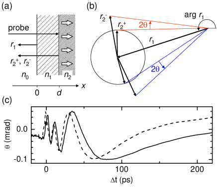
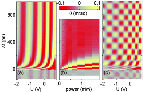
Figure 1(c) shows KR traces for sample 1 at and V, exhibiting initially fast oscillations at whose frequency decreases at higher . For more negative , oscillates faster. In Fig. 2(a), the dependency of on and is presented as a density plot. We see that for a given , reaches an asymptotic value at ns that is determined by and oscillates with . Between –2.0 and 0.8 V, about four full oscillations can be resolved.
The oscillations in with and can be explained in the context of the optical interference discussed above: The pump pulses create spin-polarized charge carriers that extend from the semiconductor surface about 2–10 m into the semiconductor. Driven by the strong electric field in the depletion layer, the spin-polarized electrons will drift into the semiconductor, whereas the holes are pushed towards the electrode. As the distance between the front of the spin-polarized electrons and the semiconductor surface increases, increases and therefore oscillates. As the electron front moves into the semiconductor, the electric field weakens and the drift slows down until the electrons reach the end of the depletion layer at , where the phase of the oscillations attains an asymptotic value that linearly depends on . Since can be varied by changing , the asymptotic value of oscillates with .
The electric field in the depletion layer is dynamically screened by the photoexcited electron-hole pairs. A variation of the pump power should affect the screening and thus the dynamics of the moving electron front, but not its end position at . This is confirmed in a measurement of the pump-power dependence of at V [Fig. 2(b)], clearly showing that although the time spacing of the oscillations varies widely with pump power, the asymptotic value at long is not affected. Dynamic screening directly affects the dielectric function through the Franz-Keldysh effect Shank et al. (1981), which could in principle also lead to oscillations in . However such oscillations would neither exhibit the observed dependence on rem (a) nor would its asymptotic phase be independent of pump powerrem (b).
Before discussing the interference mechanism further, we exclude in the following that the oscillations in are induced by the dynamics of the electron spin. For instance, the oscillations in could be induced by spin precession about an internal magnetic field due to hyperfine interaction with nuclear spins or spin-orbit effects. If this were the case, an external magnetic field would either enhance or decrease the period of the oscillations of . In Fig. 2(c), is shown with T applied in the (110) direction of the GaAs wafer. Superposed onto the same modulation of as at , now exhibits a periodic oscillation in due to spin precession about . Also, a magnetic field applied along the (100) direction does not affect the modulation of (data not shown). In fact, can be written as the product of a component proportional to the electron spin polarization and a spin-independent factor that oscillates with and .
Further insight into the origin of the modulation is obtained by studying how spins excited by an earlier laser pulse sum up with those of a new pulse. Every 12.5 ns, a pump pulse excites a new spin packet. If the spins of an old packet have precessed an integer number of cycles until a new packet is excited, the KR signal is resonantly amplified Kikkawa and Awschalom (1998). If the observed modulation of were due to spin precession, different amplifications would be expected for negative and positive upon arrival of a new pump pulse. A positive correlation would give rise to a resonant build-up, a negative one would suppress the resonance. As seen in Fig. 3(a), saturates at a positive (negative) value for mV (550 mV), T and ns (equivalent to ). For mT, the spins have precessed half a cycle, and has reversed its sign at ns. In Fig. 3(b), the -dependence of is shown at ns and for 300 and 550 mV. The peak at 0 mT is repeated at –15.5 mT, corresponding to one full precession cycle in 12.5 ns. Reversing the sign of at 12.5 ns by varying does not suppress resonant spin amplification, but only reverses its sign. This is a clear indication that the modulations of at are not related to spin precession.
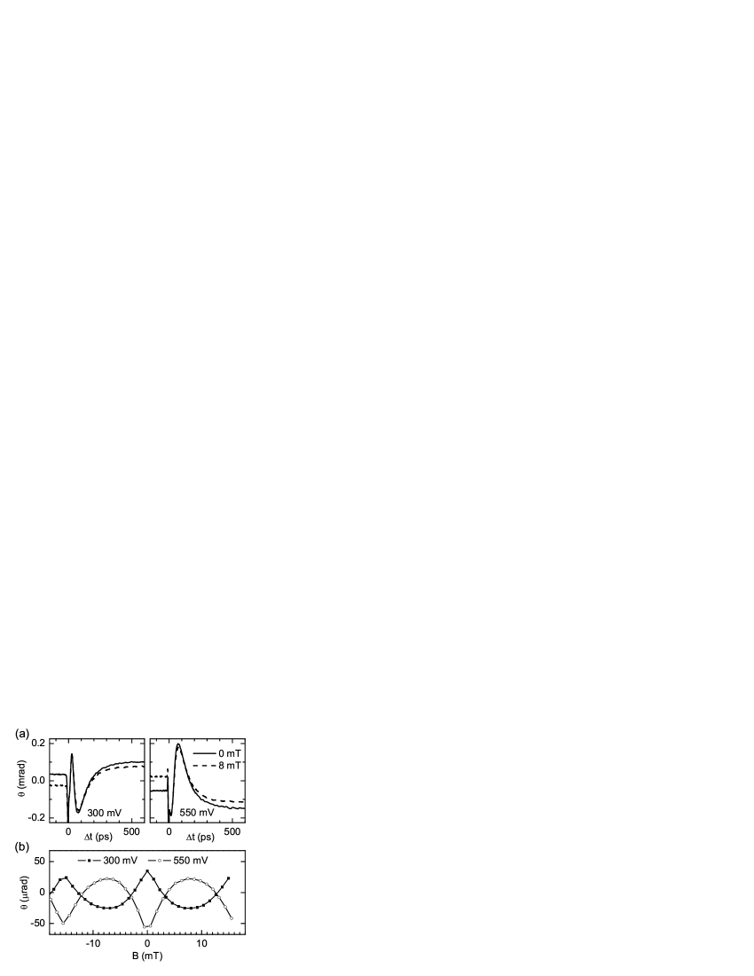
Figure 3(a) reveals the dependence of the KR signal on the spatial distribution of the electron spins: Immediately after injection of the new spin packet at , does not depend on whether the old spin packet has precessed half a turn (8 mT) or not (0 mT) rem (c). As the polarization of the old spin packet has not decayed completely, the newly excited spins must mask the old spins. This is possible because the new spin packet has a different spatial position that starts directly at the GaAs surface, whereas the old spins have already travelled behind the depletion layer. As long as the new spins are closer to the semiconductor surface than the old spins, they predominate the KR signal. The old spins will contribute to the signal and possibly resonantly amplify it once the new spins have arrived behind the depletion layer and mix with the old ones.
Assuming that the modulation in is due to an interference of the reflected beams from the metallic electrode and the front of the spin-polarized electrons at position , we obtain from the data shown in Fig. 2(a). After numbering subsequent peaks (both positive and negative ones) in by an integer , we obtain , where is an offset that depends on several quantities: The phase change of reflection and transmission at the metallic electrode, the helicity-dependent reflection at the receding front of the spin-polarized electrons, a smearing of the front due to carrier diffusion, and a correct numbering of the interferences. Using a transfer-matrix approach with literature values for the refractive indices of Au, Al, Al2O3 and GaAs, we calculate and . Surprisingly, the phases for which peaks in occur depend only on the relative strength of CD and CB, i.e. on the ratio of the real and complex parts of , and not on . This is because the contrast between and not only influences the phase of , but also the difference in and . Both contributions compensate each other in their effect on the position of maximum . Peaks in are expected at for CD and at for CB. From this and assuming , we obtain = –39 (–10) nm for predominantly CD (CB). After becomes negative at mV and ps, no new peak emerges for higher [Fig. 2(a)]. This suggests that this negative value corresponds to . At more negative , the initial oscillations start to smear out because of finite temporal resolution, and the correct numbering is obtained by extrapolation to data at positive .
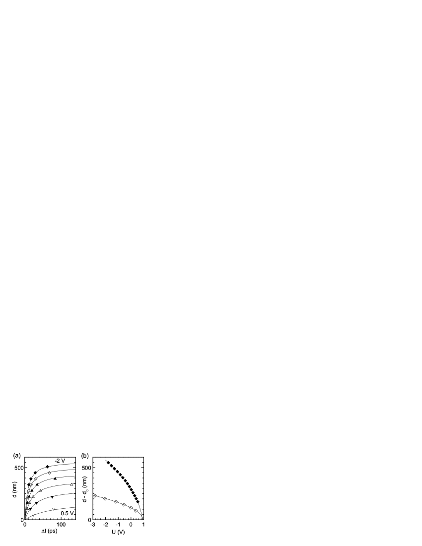
In Fig. 4(a), is plotted for sample 1 (symbols) measured at a pump power of 650 W and taking = –10 nm. The data is fitted using , which is derived from , where is the velocity of the electron front at . The latter is motivated by assuming a screening of the electric field in the depletion layer, , proportional to . Without screening, , and . The data in Fig. 4(a) are fitted by expressing and by : and . is the built-in potential across the Schottky barrier and the dielectric constant of GaAs. We find a dependence of on that can be approximated as , with cm4/V3s. We obtain = 0.75, =0.79 V, and cm-3. For V, we therefore have V/cm, nm, and cm/s. A fit with nm yields similar values, but has a higher standard deviation. The velocity is about 10 times smaller than the high-field drift velocity in GaAs Blakemore (1982) and about times smaller than , with cm2/Vs. These results are evidence of a space-charge-related origin of the observed dynamics, in which the spatially separating electrons and holes screen the electric field Dekorsy et al. (1993); Achermann et al. (2002). The screening is limited by the excited charge density, which explains the observed superlinear increase of with . As can be seen in Fig. 2(b), the screening strongly decreases as the pump power and thus the density of excited electron-hole pairs is reduced.
By numbering the oscillations of at constant , we obtain vs. . At ns, , and can be obtained [Fig. 4(b)]. The data is in excellent agreement with a fit to the analytical expression for , for which we obtain () cm-3, (0.93) V, and =-60 (0) nm for sample 1 (sample 2). The fitted is slightly higher than the nominal doping concentration, which might be related to the electron front not being completely pushed out of the depletion layer, or to a smaller dielectric constant than the assumed values (, Blakemore (1982)).
We find evidence of the interference effect also in GaAs without metallization. Note that for the position-modulated KR to occur, the only spin-sensitive contribution to the reflected probe beam must be the reflection at the electron front. Specifically, no modulation is expected in a Faraday rotation geometry and for thin epilayers where an additional reflection from the sample’s back side interferes with the measured beam.
In conclusion, we have observed that the KR signal of spin-polarized electrons in bulk -doped GaAs oscillates after optical excitation of spin-polarized electron-hole pairs. This is explained by an optical interference of the weak reflection at the receding front of the spin-polarized electron distribution with the strong reflection at the semiconductor surface. This new method allows one to directly map the position of spin-polarized electrons on a picosecond time scale and to characterize semiconductor properties of the bulk and of interfaces rem (d).
We acknowledge M. Tschudy and M. Witzig for technical support, as well as R. Allenspach, R. Mahrt and L. Meier for fruitful discussions.
References
- Shah (1999) J. Shah, Ultrafast Spectroscopy of Semiconductors and Semiconductor Nanostructures (Springer, Berlin, 1999).
- Shank et al. (1981) C. V. Shank, R. L. Fork, B. I. Greene, F. K. Reinhart, and R. A. Logan, Appl. Phys. Lett. 38, 104 (1981).
- Dekorsy et al. (1993) T. Dekorsy, T. Pfeifer, W. Kütt, and H. Kurz, Phys. Rev. B 47, 3842 (1993).
- Achermann et al. (2002) M. Achermann, F. Morier-Genoud, W. Seifert, L.-E. Wernersson, U. Siegner, and U. Keller, Phys. Rev. B 65, 045322 (2002).
- Kikkawa and Awschalom (1999) J. M. Kikkawa and D. D. Awschalom, Nature 397, 139 (1999).
- Kato et al. (2004) Y. K. Kato, R. C. Myers, A. C. Gossard, and D. D. Awschalom, Science 306, 1910 (2004).
- Crooker and Smith (2005) S. A. Crooker and D. L. Smith, Phys. Rev. Lett. 94, 236601 (2005).
- Katayama et al. (1988) T. Katayama, Y. Suzuki, H. Awano, Y. Nishihara, and N. Koshizuka, Phys. Rev. Lett. 60, 1426 (1988).
- Suzuki et al. (1998) Y. Suzuki, T. Katayama, P. Bruno, S. Yuasa, and E. Tamura, Phys. Rev. Lett. 80, 5200 (1998).
- Snelling et al. (1994) M. J. Snelling, P. Perozzo, D. C. Hutchings, I. Galbraith, and A. Miller, Phys. Rev. B 49, 17160 (1994).
- Kikkawa and Awschalom (1998) J. M. Kikkawa and D. D. Awschalom, Phys. Rev. Lett. 80, 4313 (1998).
- Salis and Moser (2005) G. Salis and M. Moser, Phys. Rev. B 72, 115325 (2005).
- rem (a) In the Franz-Keldysh effect, the dielectric function at a given oscillates with [see, e.g. M. Sydor et al., Phys. Rev. B 40, 8473 (1989)], while we observe an asymptotic phase proportional to the surface electric field , see Fig. 4(b).
- rem (b) When the electrons arrive at the end of the depletion layer, a pump-power dependent screening would still affect the phase of Franz-Keldysh oscillations until all excess electrons have recombined.
- rem (c) The decreasing amplitude of with at 8 mT can be explained by the slow precession of the spin.
- Blakemore (1982) J. S. Blakemore, J. Appl. Phys. 53, 123 (1982).
- rem (d) Also the total reflectivity is modulated by , which is measurable as an oscillation in differential reflectivity and makes it possible to map the position of unpolarized electrons.