Polariton quantum boxes in semiconductor microcavities
Abstract
We report on the realization of polariton quantum boxes in a semiconductor microcavity under strong coupling regime. The quantum boxes consist of mesas, etched on the top of the spacer of a microcavity, that confine the cavity photon. For mesas with sizes of the order of a few microns in width and nm in depth, we observe quantization of the polariton modes in several states, caused by the lateral confinement. We evidence the strong exciton-photon coupling regime through a typical anticrossing curve for each quantized level. Moreover the growth technique permits to obtain high-quality samples, and opens the way for the conception of new optoelectronic devices.
pacs:
71.36.+c, 73.21.LaConfining semiconductor structures allows the study of various fundamental effects, ranging from the Purcell effect to the full quantum confinement. Such confinement is also used for applications in many fields, from optoelectronics to quantum information. Previous works have focused on different aspects: on the one hand, on the matter part, with the confinement of the excitonic resonances in quantum wells, quantum wires and quantum dots. On the other hand, environment for the electromagnetic field has been modified by optical confinement in different types of cavities. Additionally since the middle of the 90’s, low dimensional devices have been realized in the strong coupling regime Weisbuch92 . Confinement can enhance the interactions, modify the real and imaginary parts of the resonance’s energy, or open access to new interaction processes. It is also often considered as a possible way to obtain a condensed phase of bosons in semiconductors Snoke , but so far the fermionic nature of excitons has always become dominant upon increasing density. In this sense, polaritons are of great interest as, despite their excitonic content, they have a very small effective mass in comparison to the exciton (thanks to their photonic component), which theoretically increases their temperature of condensation (above ) kavokin . The peculiar trap shape of the lower microcavity polariton dispersion curve has motivated several relaxation experiments towards the bottom of this ”trap” Baumberg00 ; Richard05 but no clear evidence for the formation of spontaneous coherence formation has been given yet.
0D Polariton confinement can be achieved either through their excitonic or through their photonic component. Recently, evidence for 0D polaritons has been given with single quantum dots in micropillars Reithmaier , photonic nanocavities Yoshie , or microdisks Peter and for a large number of excitations in micropillar structures bloch ; obert ; dasbach . Here we consider a novel system under strong coupling regime, where 0D confinement is achieved through the photonic part of polaritons in high Q cavities. Our original structure contains polariton quantum boxes, constituted by mesas in the spacer layer of a semiconductor microcavity, allowing to keep the strong coupling regime. Each mesa, by acting on the two degrees of freedom of the photonic component of the 2D cavity polaritons, does create a localized photonic box in the microcavity.
The main specificity of our technique is that the semiconductor microcavity around the mesas is in no way altered by the creation of the box, contrary to the case of etched microcavities. This brings about a number of advantages : i) the presence of the 2D cavity restricts the lateral losses for the confined mode, ii) the number of confined levels in the quantum box is controlled by the height of the mesa, iii) interaction between the 0D and the surrounding 2D polaritons is possible, iv) the technique also allows to create patterns at will, for example polariton quantum wires dasbach1D , which will allow studying possible interactions between 0D, 1D and 2D bosons.
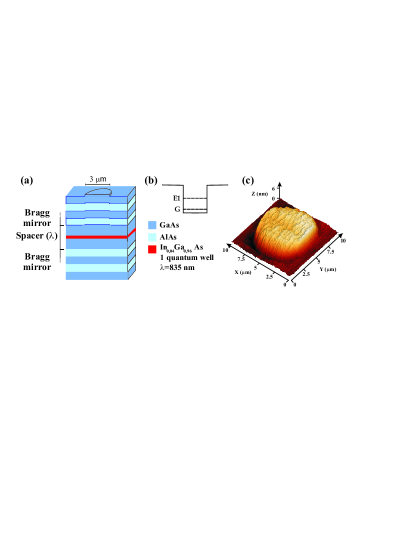
By using an original technique, we were able to fabricate microcavities with mesas etched on the spacer layer. The mesa lengthens the cavity and thus lowers the cavity mode energy (see Fig.1). This local difference creates a potential trap for the confined photons. The lateral shape and size of the mesas are defined by photolithography. The height of the mesas is determined by the etching process and can be changed at will. It has to be large enough to allow the existence of at least one confined level. Here, it has also been chosen small enough to obtain mesas and planar cavity photon modes close to the excitonic resonance. Thus we manage to observe mixed exciton-photon states inside and outside the mesas on the same part of the sample. Such a method of defining the structure, by a step of a few nanometers only, avoids any lateral losses as observed in the micro-pillar structure previously published obert .
The final structure, schematically represented with a circular mesa on Fig. 1(a), is prepared in the following way. First, we grow 22 AlAs/GaAs pairs of Distributed Bragg Reflectors (DBR), then the GaAs spacer, with a single embedded InGaAs/GaAs quantum well (QW). The quantum well with about Indium in Gallium Arsenide, is chosen to allow measurements in transmission through the wafer below the gap of GaAs HoudreAPL . Then we perform photolithography defining the pattern of the mesas, and finally the etching, which determines their height. We can design various patterns for the mesas on a single sample, but the etching process defines a common height for all of them. Let us stress that the excitonic mode is absolutely not affected by the etching process, whatever the pattern of the mesa. Finally the regrowth of the upper 21 pairs is realized again by Molecular Beam Epitaxy, after an in situ hydrogen cleaning which guarantees a perfect regrowth interface.
The high quality of the sample can be appreciated by atomic force microscopy (AFM) measurements. Fig. 1c) shows a -diameter circular mesa on the surface of the complete structure. Amazingly enough, the step height of the etched mesas is kept even after the regrowth of the thick top Bragg mirror. The abruptnesses of the steps as a function of the crystal orientation is correlated to the mobility of the elements during growth. The profile along is much steeper ( width) than along ( width), which corresponds to a slower mobility of the atoms. This gives rise to a surface asymmetry along the different crystalline orientations, with a smoothing of the etched faces that increases proportionally to the overgrowth thickness. The step height corresponds to the change of the photon mode energy that we calculated by transfer matrix simulations. According to the AFM measurement on the top mirror of a step, we compute an energy difference of , in very good agreement with the photoluminescence experiment results.
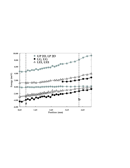
Let us first consider the properties of the microcavity, the effect of etching and regrowth. For this we measure the anticrossing curve of the resonances, resulting from the strong coupling regime of the 2D polaritons and on large square mesas of , where no confinement effect is expected, but where the photonic resonance is red-shifted due to the larger length of the cavity. The anticrossing curve is accessible using the wedge of about in this sample. This thickness variation corresponds, for a cavity, to an energy variation for the photonic resonance of about across the whole sample. In the zone of interest the variation is about . As the quantum well’s resonance is less affected by the thickness, its energy variation is below across the whole sample. The spectral properties are measured in a photoluminescence experiment. The sample, cooled to about 10K, is pumped by an Argon laser (), at low pump intensity (see below). The luminescence is analyzed with a resolution spectrometer. The microcavity features a Rabi splitting energy of , and a full width at half the maximum (FWHM) of for the photon mode, corresponding to a quality factor of , and of for the quantum well exciton. We then performed the same anticrossing measurement on the large square mesas of , disposed all along the wedge, separated by one from the other. Finally we obtained a double anticrossing curve (not shown). The two photon modes -on the mesas and around the mesas- are separated by . The photon mode shows the same linewidth on both domains. The two anticrossings have exactly the same characteristics, which guaranties that the etching process just shifts the cavity mode, as expected.
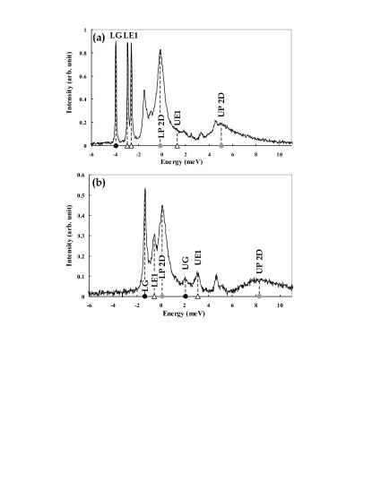
We now focus on the effect of the quantum confinement of the polaritons in cylindrical mesas of in diameter (other sizes give similar results). The laser spot diameter being , the spectra display both the confined polaritons of the mesa and the 2D polaritons of the planar cavity outside the mesa, displaced towards higher energies. Let us note that the light emission from one single quantum box is very intense, which allowed us to perform all experiments on single polariton boxes, well below the non-linear regime, in contrast to the case of pillar microcavities dasbach ; obert . We consider first the photoluminescence spectrum of a mesa relatively far from the excitonic resonance on Fig.2a). The lower polariton mode of the mesa is thus quasi-photonic and probes the quantum confinement of the photonic box. It is split into several peaks. For sake of clarity, we will only consider the ground level (G) and the first excited level (E1), which is a doublet. This doublet corresponds to a degeneracy lifting that results from the asymmetry of the mesas at the level of the spacer assymetry . This asymmetry is already present on the photolithography mask and is not linked to any growth or etching process. The quantized photonic peaks have a spectral width of about , a factor of two smaller than observed on the non-confined cavity photon mode. The smallest value measured reached , indicating a quality factor of for the confined photon modes (better than for the 2D photon modes, thanks to the additional lateral confinement). The energy of the ground level is above the energy of the bottom of the trap (as observed on the large mesas at the same position on the wedge).
To demonstrate the strong coupling even in the smallest mesas and the polariton nature of the trapped states, we systematically measured the spectra on mesas disposed along the wedge, i.e. with different detunings. For the 2D polaritons, we are always rather far from the position for which exciton and 2D cavity photon are degenerate, and the lower polariton mode stays at the exciton energy on the whole range of positions shown in Fig.3. For the confined states, strong coupling is very nicely demonstrated by the anticrossing curve for the emission of each of the two confined levels of the mesas’ polaritons. They present a Rabi splitting of around . The degeneracy lifting of the first excited level is no longer visible for the lower polariton modes when their excitonic component is too important. It is not at all visible for the upper polariton modes, due to additional relaxation channels, such as the coupling to continuum states or lower energy modes. Fig.2b) displays the photoluminescence spectrum very close to zero detuning in the trap, where lower and upper polariton modes confined in the quantum box are nicely resolved. Despite the relatively large linewidth of the 2D exciton, the high Q factor and the very efficient relaxation to the quantum boxes, allow to observe the confinement for both the lower and upper polariton states.
.
In summary, we have reported the realization of a semiconductor microcavity in strong coupling regime with embedded polariton quantum boxes. The trap consists of a mesa in the spacer layer, obtained by a well controlled technique. To our knowledge, this is the first time that quantum confinement is resolved simultaneously for both upper and lower polariton modes, and that the anticrossing is resolved separately for all the quantized polaritons. Experimental and theoretical work on the dispersion of the quantized modes is being performed. The co-existence in the same sample of 2D and 0D polaritons, as well as the possibility to study a single quantum box, will allow original studies such as resonant parametric scattering or trapping by spatial relaxation. Wide possibilities in the transverse shape of the mesas also open the way to the realization of various experimental configurations for the bosonic polariton states, which energy, wavefunction and dimensionality can be engineered on demand.
We would like to acknowledge fruitful discussions with C. Ciuti, P. Lugan, M. Saba, and V. Savona. We are thankful for the strong financial support from the Swiss NCCR research program Quantum Photonics.
References
- (1) C. Weisbuch, M. Nishioka, A. Ishikawa et Y. Arakawa, Phys. Rev. Lett. 69, 3314 (1992).
- (2) S. A. Moskalenko and D. W. Snoke, Bose-Einstein Condensation of Excitons and Biexcitons and Coherent Nonlinear Optics with Excitons (Cambridge University Press, Cambridge, 2000).
- (3) A. Kavokin, G. Malpuech and F.P. Laussy, Phys.Lett. A 306, 187 (2003).
- (4) J. J. Baumberg, P. G. Savvidis, R. M. Stevenson, A. I. Tartakovskii, M. S. Skolnick, D. M. Whittaker,and J. S. Roberts, Phys. Rev. B 62, R16247 (2000).
- (5) M. Richard, J. Kasprzak, R. Romestain, R. André and Le Si Dang Phys. Rev. Lett. 94, 187401 (2005).
- (6) J. P. Reithmaier, G. Sek, A. Löffler, C. Hoffmann, S. Kuhn, S. Reitzenstein, L. V. Keldysh, V. D. Kulakovskii, T. L. Reinecke and A. Forchel, Nature 432, 197 (2004).
- (7) T. Yoshie, A. Scherer, J. Hendrickson, G. Khitrova, H.M. Gibbs, G. Rupper, C. Ell, O. B. Shchekin and D. G. Deppe, Nature 432, 200 (2004).
- (8) E. Peter, P. Senellart, D. Martrou, A. Lemaître, J. Hours, J.-M. Gérard and J. Bloch, Phys. Rev. Lett. 95, 067401 (2005).
- (9) J. Bloch, F. Boeuf, J.-M. Gérard, B. Legrand, J.-Y. Marzin, R. Planel, V. Thierry-Mieg, and E. Costard, Physica E 2, 915 (1998).
- (10) M. Obert, J. Renner, A. Forchel, G. Bacher, R. André, and D. Le Si Dang, Appl. Phys. Lett 84, 1435 (2004).
- (11) G. Dasbach, M. Schwab, and A. Forchel, Phys. Rev. B 64, 201309(R) (2001).
- (12) G. Dasbach, A.A. Dremin, M. Bayer, V.D. Kulakovskii, N.A. Gippius, and A.Forchel, Phys. Rev. B 65, 245316 (2002).
- (13) They have an elliptical shape with an absolute difference of about between the small and the large axis. This asymmetry is given by the pattern we designed on the photolithography mask.
- (14) R. P. Stanley, R. Houdré, U. Osterle, M. Gailhanou, and M. Ilegems, Appl. Phys. Lett. 65, 15 (2004).