The Effect of Transfer Printing on Pentacene Thin-Film Crystal Structure
Abstract
The thermal deposition and transfer Printing method had been used to produce pentacene thin-films on SiO2/Si and plastic substrates (PMMA and PVP), respectively. X-ray diffraction patterns of pentacene thin films showed reflections associated with highly ordered polycrystalline films and a coexistence of two polymorphs phases classified by their d-spacing, d(001): 14.4 and 15.4 .The dependence of the c-axis correlation length and the phase fraction on the film thickness and printing temperature were measured. A transition from the 15.4 phase towards 14.4 phase was also observed with increasing film thickness. An increase in the c-axis correlation length of approximately 1216% was observed for Pn films transfer printed onto a PMMA coated PET substrate at 100 120 oC as compared to as-grown Pn films on SiO2/Si substrates. The transfer printing method is shown to be an attractive for the fabrication of pentacene thin-film transistors on flexible substrates partly because of the resulting improvement in the quality of the pentacene film.
I Introduction
Pentacene (C22H14), a linear acenic hydrocarbon composed of five benzene rings[1,2], has received considerable interest as the active layer for organic thin-film transistors (TFTs). This is due to the strong tendency of pentacene (Pn) to form an ordered film that exhibits superior transport properties[3,4]. To make organic TFTs with high mobility, it is very important to fabricate highly ordered pentacene films with large sized crystal domains[5], and low defect density[6]. Several fabrication methods, for example thermal evaporation[7, 8,9,10], growth from solution[10,11], have been used to grow Pn on various non-organic substrates, such as SiO2 [9,12], carbon[13], Kapton[10,14] and NaCl[17]. Previous structure studies by X-Ray diffraction (XRD)[10,11,12,17] and electron diffraction (ED)[10,15] found at least four polymorphs of Pn. They are classified by their layer spacing, d(001)[10] : 14.1[11,16], 14.4[1,2], 15.1[17], and 15.4 [9, 12,18]. The 14.1 structure was commonly referred to as the single crystal phase . The 15.1 and 15.4 were referred to as the thin film phase . The 14.4 phase was first identified by Campbell et al.[1,2] by using a film method. It was also called a single crystal phase [5, 8 ,9, 12, 18, 20] in the past. However Mattheus et al.[10] showed that this phase should be designated as thin film phase . The unit cell parameters [10, 15,17,21] and the stacking of the molecules within the layer, which affect the electronic properties of Pn[6, 22], were also studied.
Currently, research efforts addressing pentacene are being driven by an interest in developing and improving high-quality organic thin-film devices for low cost fabrication on flexible organic substrates[19]. Hines et al. have recently reported that an adaptation of Nano-imprint lithography (NIL) [23, 24] called Nano-Transfer Printing[ 25], can be used to create high-quality organic TFTs on flexible substrates. The pentacene TFTs exhibited a field-effect mobility as high as 0.09 cm2 (Vs)-1and an on/off ratio of 104 [25].
In this paper, we present XRD studies of pentacene films deposited on SiO2/Si and printed onto PMMA and PVP substrates as a function of film thickness, printing temperature, and printing time. We have observed the co-existence of the 14.4 and 15.4 phases And an increase in the c-axis correlation length (i.e. Pn film quality perpendicular to the substrate surface) introduced by the transfer printing.
II Experiments
Pentacene films with different film thicknesses deposited on (SiO2)/Si wafers were fabricated by thermal deposition in a high vacuum evaporation chamber. The Si001 wafers with a 300 nm thermal oxide surface (SiO2) were used as a transfer substrate in a subsequent transfer printing process. The Pn films on a PMMA/PET substrate were fabricated by the transfer printing method. The 200 nm thick PMMA surface coating was spin coated on PET at 4000 rpm for 60 sec and baked on a 90 oC hotplate for 3 minutes. prior to the transfer printing. The PET substrate was a DuPont Molinex@ 453 film, with an ITO coating on the back surface. The transfer printing was done with a Nanonex NX2000 imprinter at a fixed printing pressure (100 psi) with different printing control parameters, such as temperature and time. The details of the transfer printing process have been addressed elsewhere[25].
The out-of-plane structure of the pentacene films was determined using X-ray diffraction in a coupled -2 reflection geometry. Ultra high-resolution XRD studies were performed using a Rigaku UltraX18 rotating anode generator equipped with a Huber 4-circle diffractometer system. The x-ray source used was CuK Data acquisition was performed with a uniform X-ray power of 14 kW and a selectable scanning dwell time. All the measurements were performed at room temperature under ambient conditions.
III Results and Discussion
The structural properties of pentacene films were studied as a function of layer thickness and transfer printing temperature. Figure 1 shows the XRD patterns of 0.05, 0.25, 0.5 and 1 m pentacene thin-films deposited on SiO2 /Si substrates prior to transfer printing. The reflection intensities are plotted vs. the scattering vector q (-1), where
| (1) |
The d-spacing was calculated from the inverse of the slop in a q-plot [27].
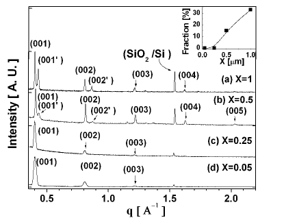
In figures 1(a)-(d), a set of sharp reflections associated with the Pn film are present in these x-ray patterns and can be indexed as (00n) reflections, with the (001) plane d-spacing equal to 15.400.4 . Also in Figs. 1(a)&(b), a second set of sharp reflections are visible in the 0.5 and 1.0 m thick films that can be indexed as (00n’) reflections with a (001’) plane d-spacing of 14.400.03 . The first time observation of the two-phase coexistence was by Dimitrakopoulos[18] who used a SiO2 substrate. Additional experiments showed that the 14.4 and 15.4 phases are substrate-induced[10]. They are commonly found in Pn films onSiO2 substrate[9, 12] and with large film thickness[5, 10, 18] and high growth temperature[5, 10]. With an increase in Pn film thickness, the intensity of reflections associated with the 15.4 phase decreases and the intensity of reflections associated with the 14.4 phase increases. In Fig. 1 inset (as grown Pn on SiO2/Si), the volume fraction of the 14.4 phase increased from 0 % for the 0.05 m and 0.25 films to 15% for the 0.5 m film and 33% for the 1.0 m film. This observation agrees with previous results[5, 10, 12, 18].The volume fraction here is defined as the ratio of relative intensity of the 14.4 phase to the total intensity for the (001) reflections[19].
Figures 2(a)-(e) show the XRD patterns of 0.5 m Pn thin films before and after having been transfer printed onto a PMMA coated PET substrate with printing conditions of 100 psi at 100, 120 and 140 oC for 3 min. and onto a PVP coated PET substrate with printing temperature 140 oC.
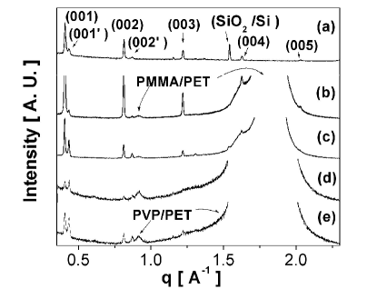
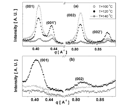
The two phase co-existence of the14.4 and 15.4 phases persisted through the transfer printing process. The unchanged d(001) spacing indicates that the transfer printing did not affect the rotation of pentacene molecules along [001] direction[17, 21]. A decrease in intensity of the reflections associated with the 15.4 phase and an increase in intensity of the reflections associated with the 14.4 phase are visible with increasing printing temperature. At 100, 120, and 140 oC, the volume fractions of the 14.4 phase on the PMMA substrate are 5, 30, and 55% respectively. At 140 oC, the volume fraction of the 14.4 phase on the PVP/PET substrate is 45%. Figure 3 shows the expanded XRD patterns of the first and second reflections of 0.05 m and 0.5 m pentacene films on a PMMA substrate. Clearly, the 14.4 phase volume diffraction depended on the nature of the substrate, film thickness and printing temperature. It is more thermally stable than 15.4 phase.
To study the crystal perfection along the growth direction (c-axis), we calculated the crystalline grain size of the Pn films perpendicular to the substrate surface using Para-crystal theory[28]. Since the (00n) planes are parallel to the substrate, this theory can provide a calculation of the average grain size (c-axis correlation length) in the direction normal to the substrate surface. The broadering equation is given by
| (2) |
where
is the overall broadening of the nthx-ray reflection. (s)c is the broadening due to the average grain size and (s)II is the broadening due to the structural disorder gII. Also is the half width of the peak at half maximum as calculated from a Gaussian fit. The (s)2values are plotted in Fig. 4(a) as a function of n4 for the 15.4 phase of 0.05, 0.25, 0.5 and 1 m pentacene thin-films deposited on SiO2/Si (filled data points) and transfer printed onto the PMMA substrate (open data points). The average crystalline grain size parameters Lhkl and gII were calculated from the ordinate intercept and the slop of the lines from a fit of Eq. 2 to the data points in Fig. 4(a). The calculated average grain sizes for the Pn films on SiO2/Si substrates prior to transfer printing are shown in Fig. 4(b) (filled data points) and are 2279 (15 monolayer (ML)), 40916 (27 ML), 67327(44 ML), and 80532 (52 ML) for the film thickness of 0.05, 0.25, 0.5, and 1 m respectively. We didn t find any reflections related to 0.25 m pentacene on PMMA/PET with printing conditions of 100 psi at 100oC for 3 min. The reason is not clear. It may due to the damage of the sample during transfer printing process. For comparison, the calculated average grain sizes for the Pn films on PMMA/PET substrates after transfer printing are also shown in Fig. 4(b) (open data points). For the transfer printed films with thickness 0.05, 0.5 and 1 m, the corresponded average grain sizes are 26311 (17 ML), 75030 (49 ML) and 907 36 (59 ML) respectively. For the above calculations, the instrumental broadening (determined from the broadening of (004)) reflection of the single crystal Si) has been subtracted from the x-ray diffraction peak widths. The term gIIis about 14% for both the as-grown and transfer printed Pn films which indicates that the structural perfection along the c-axis direction is high and unaffected by the transfer printing. Figure 4(b) shows that after transfer printing at 100 oC, the average crystalline grain sizes of pentacene thin films increase by about 1216 %.
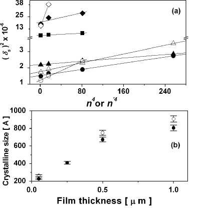
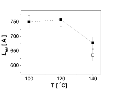
To investigate the influence of the printing temperature on the film crystalline grain size, 0.5 m pentacene films were printed at temperatures of 100, 120, and 140 oC for 3 minutes each. Figure 5 shows the calculated c-axis correlation length as a function of printing temperature on PMMA (filled data point) and PVP substrates ( open data point). Above 120 oC an increase in printing temperature leads to a decrease of the average crystalline grain size (from 75823 at 120 oC to 67820 at 140 oC). The crystalline grain size of pentacene printed at 140 oC is close to that of the original film on the SiO2/Si substrate prior to transfer printing but with a higher fraction of bulk crystal phase.
To determine the influence of printing time, pentacene films were printed at 100 oC for 3 and 30 minutes. No strong evidence showing a change in c-axis correlation length with printing time was observed.
IV Conclusions
In summary, we have studied the structure and calculated the average crystallite grain size of transfer printed pentacene films as a function of substrate, film thickness and printing temperature. For small film thickness Pn films showed only 15.4 phase. For larger film thickness, the 14.4 phase appeared and coexisted with 15.4 phase. The volume fraction of the 14.4 phase increases with increasing film thickness. This trend persisted during the transfer printing. The volume fraction of the 14.4 phase increased with printing temperature. Transfer printing at 100 and 120 oC improves the c-axis correlation length of Pn films printed onto a PMMA coated PET substrate. Longer printing times did not contribute any measurable improvement. Generally, transfer printing a pentacene film from a SiO2/Si substrate to a plastic substrate (PMMA/PET) increased the crystalline grain size by approximately 1216 % at the lower printing temperatures (100 -120 oC). This improvement in the c-axis correlation length of the transfer printed Pn films highlights an important advantage of the transfer printing method and adds to the attractiveness of this technique for the fabrication of high quality pentacene thin films on plastic substrates.
Acknowledgements.
This work was supported in part by NSF Grant No. ECS-0329347 and by the Laboratory for Physical Sciences, University of Maryland.References
- (1) R. B. Campbell, J. Monteath Robertson, and J. Trotter, Acta Cryst., 14, 705 (1961).
- (2) R. B. Campbell and J. Monteath Robertson, Acta Cryst. 15, 289 (1962).
- (3) T. W. Kelly, L.D. Boardman, T. D. Dunbar, D. v. Muyres, M. J. Pellerite, and T. P. Smith, J. Phys. Chem. B, 107, 5877 (2003).
- (4) S. Scheinert, G. Paasch, M. Schr dner, H. K. Roth, S. Sensfu , and Th. Doll, J. Appl. Phys. , 92, 330 (2002).
- (5) B. Stadlober , V. Satzinger, H. Maresch, D. Somitsch, A. Haase, H. Pichler, W. Rom, and G. Jakopic, , Proceedings of SPIE, Organic Field Effect Transistors II. , 5217, 112 (2003).
- (6) B. Nickel, R. Barabash, R. Ruiz, N. Koch, A. Kahn, L. C. Feldman, R. F. Haglund and G. Scoles, Phys. Rev. B , 70, 125401 (2004).
- (7) D. Knipp, R. A. Street, A. V lkel, and J. Ho, J. Appl. Phys. , 93, 347 (2003).
- (8) J. Lee, J. H. Kim, S. Im, and D. Y. Jung, J. Appl. Phys. , 96, 2301 (2004).
- (9) D. J. Gundlach, T. N. Jackson, D. G. Schlom and S. F. Nelson, Appl. Phys. Lett. , 74,3303 (1999).
- (10) C. C. Mattheus, A. B. Dros, J. Baas, G, T. Oostergetel, A. Meetsma, J. L. de Boer and T. T. M. Palstra, Synthetic Metals, , 138, 475 (2003).
- (11) D. Holmes, S. Kumaraswamy, A. J. Matzger, and k. P. C. Vollhardt, Chem. Eur. J., 5, 3399 (1999).
- (12) I. P. M. Bouchoms, W. A. Schoonveld, J. Vrijmoeth, and T. M. Klapwijk, Synthetic Metals,, 104, 175 (1999).
- (13) L. F. Drummy and D. O. Martin, Adv. Mater. , 17, 903 (2005).
- (14) S. E. Fritz, S. M. Martin, C. D. Frisbie, M. D. Ward and M. F. Toney, J. Am. Chem. Soc., 126, 4084 (2004).
- (15) L. F. Drummy and D. O. Martin, Adv. Mater. , 17, 903 (2005).
- (16) C. C. Matteus, A. B. Dros, J. Baas, A. Meetsma, J. L. de Boer and T. T. M. Palstra, Acta Cryst. C, , 57, 939 (2001).
- (17) J. S. Wu and J. C. H. Spence, J. Appl. Cryst., 37, 78 (2004).
- (18) C. D. Dimitrakopoulos, A. R. Brown, and A. Pomp, J. Appl. Phys. , 80, 2501 (1996).
- (19) B. Stadlober , V. Satzinger, H. Maresch, D. Somitsch, A. Haase, H. Pichler, W. Rom, and G. Jakopic, Proceedings of SPIE, Organic Field Effect Transistors II. 5217, 112 (2003).
- (20) J. Puigdollers, C. Voz, A. Orpella, I. Martin, M. Vetter and R. Alcubilla, Thin Solid Films, 427, 367 (2003).
- (21) C. C. Mattheus, G. A. de Wijs, R. A. de Groot and T. T. M. Palstra, J. Am. Chem. Soc., 125, 6323 (2003).
- (22) R. C. Haddon, X. Chi, M. E. Itkis, J. E. Anthony, D. L. Eaton, T. Siegrist, C. C. Mattheus, and T. T. M. Palstra, J. Phys. Chem. B, 106, 8288 (2002).
- (23) S. Y. Chou, P. R. Krauss, and P. J. Renstrom, Appl. Phys. Lett. , 67, 3114 (1995).
- (24) T. Borzenko, M. Tormen, G. Schmidt, L. W. Molenkamp, and H. Janssen, Appl. Phys. Lett. , 79, 2246 (2001).
- (25) D. R. Hines, S. Mezhenny, M. Breban, E. D. Williams, V. W. Ballarotto, G. Esen, A. Southard, and M. S. Fuhrer, , Appl. Phys. Lett., 86, 163101 (2005).
- (26) K. D. Knudsen, J. O. Fossum, G. Helgesen, and V. Bergaplass, J. Appl. Cryst. , 36, 587 (2003).
- (27) D. R. Hines and S. A. Solin, Phys. Rev. B , 61, 11348 (2000).
- (28) R. W. G. Wyckoff, Crystal structures,2nd ed., Interscience, New York, 1971