EXTRAORDINARY PHENOMENA IN SEMICONDUCTOR-METAL HYBRID NANOSTRUCTURES BASED ON BILINEAR CONFORMAL MAPPING
I INTRODUCTION
The recent discovery by Solin and co-workers of the phenomenon of extraordinary magnetoresistance (EMR) in hybrid structures of narrow-gap semiconductors and non-magnetic metals Solin:2000 portends considerable promise for impacting magnetic sensor technology for macroscopic, microscopic and nanoscopic applications. Solin:2001 It has been recently realized by Solin and his colleagues that the EMR phenomenon, is but one example of a broad class of geometry-based interfacial effects in hybrid structures formed from the juxtaposition of a semiconductor such as InSb, InAs Moller:2002 or Hg1-xCdxTe Solin:1996 with a metal such as Au. Indeed, one can envision a number of other ”EXX” interfacial effects in metal semiconductor hybrid structures where E = extraordinary and XX = piezoconductivity, optoconductivity, electroconductivity, thermoconductivity etc. and combinations of these such as magnetothermoconductivity. Both EPC Rowe:2003 and EOC Wieland:1 have recently been demonstrated.
The EXX effects form the basis for a number of new macroscopic and nanoscopic sensor devices analogous to those such as automobile ignition sensors and ultra-high-density read-head sensors, respectively, that derive from the discovery of the EMR phenomena. Several of the applications of EXX sensors that one can envision, especially in the field of medicine, require scaling of an EXX structure to nanoscopic dimensions. This has already been achieved in the case of EMR sensors and devices with dimensions of order 20 nm have been shown to exhibit new mesoscopic physics effects and to exhibit very high values of EMR. Solin:2002 However, the underlying principal on which the scaling of internally shunted macroscopic EXX structures to externally shunted working devices in the nanoscopic size regime has to date not been fully elucidated. Accordingly, we describe here the bi-linear conformal mapping procedure that has been applied to the scaling of EMR devices and show how that procedure can be applied to EXX structures in general.
II BACKGROUND
There are two principal contributions to the magnetoresistance of any resistive device, namely a physical contribution and a geometric contribution. Popovic:1991 The physical contribution derives from the dependence of intrinsic material properties such as carrier concentration and carrier mobility on the applied magnetic field. The geometric contribution is an extrinsic property that depends on the shape of the device, the placement and geometry of the (metallic) contacts and, the placement and geometry of any inhomogeneities or shunts that may be present. The geometric contribution to the MR also depends on the intrinsic physical properties of the inhomogeneities relative to those of the host material, e.g. on the conductivity ratio. Tineke:1998 For most materials of current interest as MR sensors such as layered magnetic metals which exhibit giant MR (GMR) Egelhoff:1995 or tunnelling MR (TMR) Mitra:2001 and the magnetic layered oxide manganites which exhibit colossal MR (CMR), Jin:1994 the physical contribution to the MR is dominant. However, Solin and his colleagues have shown that judiciously designed hybrid structures composed of a non-magnetic narrow-gap semiconductor matrix with high carrier mobility and a non-magnetic metallic inhomogeneity or shunt can exhibit a room temperature MR that is not only dominated by the geometric contribution but also attains room temperature values of order 1,000,000%. Solin:2003 This is several orders of magnitude higher than what has been achieved with conventional GMR, TMR or CMR devices. The new phenomenon was subsequently dubbed extraordinary MR or EMR. Zhou:2000
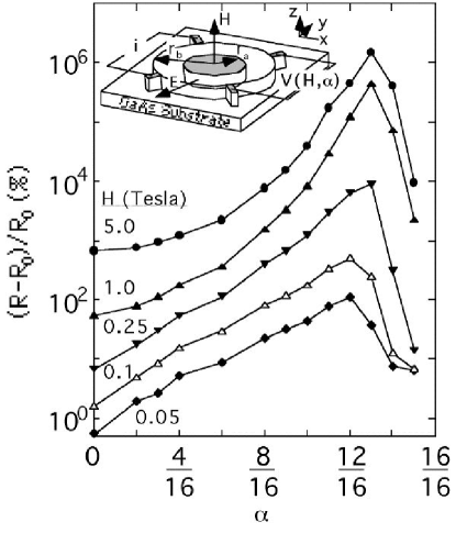
The proof of principal demonstration of EMR was accomplished with symmetric 4-probe macroscopic van der Pauw (vdP) disc structures formed from Te- doped InSb (electron concentration cm-3 and mobility cm2/Vs) containing a concentric cylindrical metallic inhomogeneity as depicted in the inset of Fig. 1. Solin et al. also showed Solin:2004 that in general,
| (1) |
where is the applied field normal to the plane of the device, is the effective field-dependent resistance measured in a 4-probe configuration is the bias field and is the applied or signal field (not the field gradient). In the zero bias large signal but low field limit, ,
| (2) |
Here and are, respectively, symmetric and antisymmetric geometric factors that depend on the shape, location and physical properties of the conducting inhomogeneity and contacts while . [For the symmetric structure shown in the inset of Fig. 1. .] Clearly, narrow-gap high mobility semiconductors such as InSb are choice materials for EMR devices.
The magnetotransport properties of the macroscopic vdP structure shown in the inset of Fig. 1. can be quantitatively accounted for using the above equations together with both finite element analysis Moussa:2001 and analytic techniques. Zhou:2001 However, the EMR phenomenon can also be readily understood using a simple though non-intuitive classical physics analysis. The components of the magnetoconductivity tensor for the semiconductor are , and with and all other tensor components being zero. If the electric field on the vertical surface of the inhomogeneity is , the current density is . The electric field is everywhere normal to the equipotential surface of a highly conducting inhomogeneity. At , is diagonal so and the current flows into the inhomogeneity which acts as a short circuit. At high (), the off-diagonal components of dominate so , and JE. Equivalently, the Hall angle between the electric field and the current density approaches 90o, and the current becomes tangent to, i.e. deflected around, the inhomogeneity. Thus, the inhomogeneity acts as an open circuit. The transition of the inhomogeneity from short circuit at low to open circuit at high results in a geometric enhancement of the MR of the semiconductor even if its resistivity (conductivity) is field-independent (i.e. the physical MR is zero).
Unfortunately, the internally shunted EXX structure shown in the inset of Fig. 1 is not conducive to fabrication on the nanoscopic scale because it is difficult if not impossible to properly embed or fill a nanoscopic hole with metal while maintaining good electrical contact with the quasi-vertical sidewall. Fortunately, as we now demonstrate, one can construct an externally shunted metal-semiconductor hybrid structure that is not only galvanomagnetically equivalent to the circular structure shown in the inset of Fig. 1, but is also “fabrication friendly” on the nanoscale.
III CONFORMAL MAPPING
It is known Popovic:1992 that any homogeneous device with a circular boundary of unit radius in the imaginary two dimensional complex -plane with orthogonal axes and where can be mapped into the complex upper half Cartesian -plane with orthogonal axes and where [see Fig. 2a)] by using the bilinear transformation Popovic:1992
| (3) |
The above mapping equation transforms the four symmetrically spaced electrical contacts on the perimeter of the disk in the -plane [shown in Fig. 2a) in the configuration for a magnetoresistance measurement] to the corresponding contacts on the line in the -plane. Although the mapped contacts are symmetric about the line they are not of equal size as they are when viewed in the -plane. If one embeds an off-centered hole of radius r1 into the homogeneous disk of
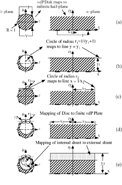
Of the structures depicted in Figs. 2a) - 2d), that shown in Fig 2b) is the simplest one which contains a fully enclosed inhomogeneity, e.g. a circular hole displaced from the center of the disk. If we embed this hole with a highly conducting metal, then the resultant structure which we call an off-center vdP disk is similar to the centered vdP disk which yielded the large EMR values cited above. However, the corresponding rectangular mapped structure in the -plane would be of infinite extent in the and directions and would contain an external shunt of infinite height in the direction. To avoid these complications, we define a structure which contains not only the cuts of Fig. 2d) but also an additional circle of radius in the -plane as shown in Fig. 2e). The latter maps to the line in the -plane. The modified off-centered vdP disk now contains a metallic inhomogeneity embedded into the space between the circles of radii , and while the space between the circle of radius and the disk perimeter contains a narrow-gap semiconductor. Thus, the -plane disk with an INTERNAL embedded shunt maps to a rectangle in the -plane with a corresponding EXTERNAL metallic shunt. Moreover, for the exact mapping depicted in Fig. 2 e), the electrical behavior of the two structures will be identical. Popovic:1991
Although the mapping technique described above has been known Popovic:1991 , the adaptation of this technique to the design of rectangular structures with external shunts has not been previously considered. Furthermore, for mapped plates with , the cuts represented by the circles of radius in the left panel of Fig. 2e) are small/negligible. Therefore, the externally shunted plate structure shown on the right panel of Fig 2e) is, to a good approximation, electrically equivalent to the vdP disk shown in the left panel of Fig. 2e) without the cuts. Moreover, an expression for the filling factor of the rectangular EXX structure, though more complex than that of the concentric circular structure has been derived as a function of the geometric properties of the structure. Zhou:2001
IV EXPERIMENTAL CONFIRMATION OF THE MAPPING PROCEDURE
In order to confirm that the mapping procedure described above is viable we test it using macroscopic EMR structures. The EMR of a non-biased macroscopic (long dimensions mm) vdP plate formed from InSb and Au is shown in Fig. 3 as a function of the geometry of the metallic shunt and of the placement of the current and voltage leads. The material constituents of the externally shunted rectangular
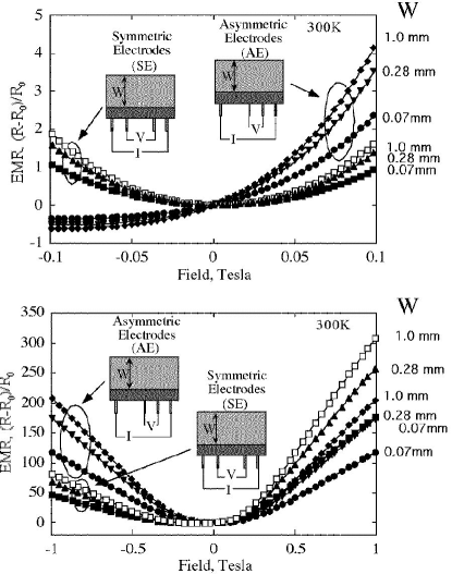
semiconductor-metal hybrid structures depicted in Fig. 3 were the same as those used for the internally shunted circular hybrid structures depicted in Fig. 1. Two features are noteworthy in the data of Fig. 3.: a) the room-temperature EMR is very large reaching values as in excess of 100% at a field of 500 Gauss. b) The EMR is asymmetric with respect to the applied field when the leads are placed asymmetrically on the rectangular narrow-gap-semiconductor plate. The latter feature constitutes a condition of self-biasing which is important for a number of applications in which the sign of the applied magnetic field must be determined.
The magnetotransport properties of the externally shunted vdP plate clearly depend strongly on the placement of the current and voltage leads, e.g. on lead geometry. These properties also depend strongly on the shape and relative dimensions of the semiconductor and metal components of the hybrid structure itself as can be seen from the dependence of the EMR in Fig. 3 on the width, , of the shunt for a semiconductor region of fixed width. Note that in the range of filling factors addressed in Fig. 3 which is below the optimum filling factor of 13/16 as depicted in Fig. 1, the EMR systematically increases with increasing filling factor. In addition, an added feature of the data of Fig. 3 is the enhancement of the EMR in the structure with asymmetric leads relative to the structure with symmetric lead placement.
V VALIDATION OF MAPPING TO THE NANOSTRUCTURE REGIME
Having established that extremely high values of EMR can be obtained from macroscopic semiconductor-metal hybrid structures, we now address the challenge of scaling such EMR devices to the nanoscopic sizes required for ultra-high-spatial resolution and high sensitivity detection of magnetic fields. To achieve high spatial resolution in the vertical direction (normal to the plane of the EMR structure) it is necessary to use ultra thin semiconductor films.
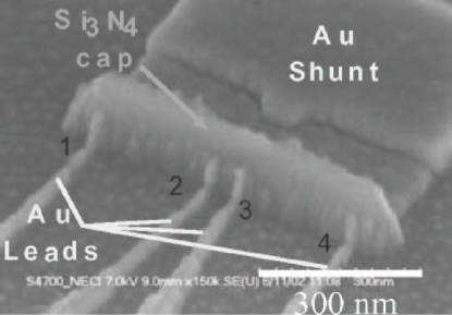
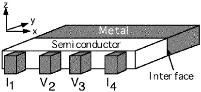
Homogeneous InSb on GaAs is not suitable for this purpose because dislocations at the semiconductor substrate interface cause a drastic reduction in the carrier mobility, and concomitantly the EMR which scales with the square of the mobility, when the thickness of the semiconductor drops below 1 m. Stradling:1991 To overcome this, Solin and coworkers used a quantum well structure, InSb/InAl1-xSbx, and state of the art suspended mask e-beam lithography incorporating a new type of resist, calixarine, to fabricate the structure shown in Fig. 4. Solin:2003 Details of the fabrication method are provided elsewhere. Solin:2002 Note that the structure shown in Fig. 4 is a nanoscopic version of the structure depicted in Fig. 2(e).
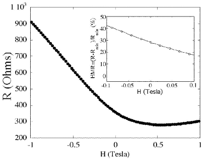
The field dependence of the room temperature magnetoresistance of the externally shunted nanoscopic EMR device shown in Fig. 4 is shown in Fig. 5. As can be seen, the EMR reaches values as high as 5 % at a signal field of 0.05 T. To our knowledge, this is the highest room temperature MR level obtained to date for a patterned magnetic sensor with this spatial resolution. Moreover, with a modest bias field of 0.2 T corresponding to the zero-field offset Solin:1997 in Fig. 5, the measured EMR is 35% at a signal field of 0.05 T. [The offset is associated with the asymmetric placement of the leads.] Also note that the device can be biased into a field region where the EMR response is linear with field, a feature that can simplify signal amplification. Equally significant is the fact that the current sensitivity, at a magnetic field bias of 0.2 T has a large measured value of 585 /T at room temperature. It is this figure that enters directly into the calculation of the power signal to noise ratio Weissman:1988 which is found from the data of Fig. 5 to be 44.5 dB for a bandwidth of 200 MHz and a signal field of 0.05 T at a bias of 0.2 T. [Note: It is common but incorrect practice in some parts of the layered metals community to use MR as the figure of merit but the proper measure should be the power signal to noise ratio at the operating bandwidth. The latter contains the MR but depends on other factors as well.]
VI EXTENSION OF MAPPING TO OTHER EXX PHEMOMENA
As noted in the introduction, EMR is but the first example of a general class of phenomena collectively referred to as EXX phenomena. To elucidate this point consider Fig. 6 which shows a three dimensional view of the hybrid structure depicted in Fig. 2(e).
The 4-probe effective resistance of this composite structure is , where and represent current and voltage probes, respectively. Now will depend on the relative conductivities of the metal and semiconductor (typically ), on the interface resistance between them and on the specific placement of the current and voltage probes (e.g. on the geometry). In a non-perturbed state, the highly conducting metal acts as an effective current shunt, provided that the interface resistance is low, and of the composite structure can be close to that of the metal. If a relatively small external perturbation such as an applied magnetic field, electric field, strain, temperature change etc. significantly alters the interface resistance and, thus, the current flow across the interface, this alteration can manifest itself as a large change in the effective resistance or, equivalently, in the output voltage (signal) of the “sensor” for that particular external perturbation.
We have illustrated this point with the EMR example where we understand the detailed physics of the mechanism by which the applied field perturbs the interface resistance. However, from an empirical viewpoint, other perturbations such as a strain field, photon field, etc. which perturb the interface resistance will yield a signal (voltage response) that is geometrically amplified by the hybrid structure. Thus the fabrication advantage for preparing an EMR nanostructure with desirable properties, is also applicable to other EXX phenomena when mapped to nanostructures of the type shown in Fig. 6.
VII CONCLUSIONS
We have shown that bilinear conformal mapping can be used to transform 4-lead internally shunted EMR semiconductor-metal hybrid structures to galvanomagnetically equivalent externally shunted 4 lead structures. The latter are compatible with the fabrication of nanoscale EMR devices while the former are not. Mapped rectangular EMR van der Pauw plate exhibit very large EMR values in both macroscopic and nanoscopic form. We have also shown that the mapping procedure applied in the case of EMR will also be applicable to other generalized EXX structures.
VIII ACKNOWLEDGMENTS
This work was supported by the U.S. National science foundation under grant ECS-0329347. I grateful acknowledge useful collaboration with A.C.H. Rowe, D.R. Hines and T. Zhou.
References
- (1) S.A. Solin, Tineke Thio, D.R. Hines and J.J. Heremans, Science 289, 1530 (2000).
- (2) S.A. Solin, and D.R. Hines, J. Magnetism. and Magnetic Materials, 226 –230, 1976 (2000).
- (3) C.H. Moller, O. Kronenwerth, D. Grundler, W. Hansen, Ch. Heyn and D. Heitmann, Appl. Phys. Lett. 80, 3988 (2002).
- (4) S.A. Solin, Tineke Thio, J.W. Bennett, and D.R. Hines M. Kawano, N. Oda, and M. Sano, Appl. Phys. Lett. 69, 4105 (1996).
- (5) A. C. H. Rowe, D. R. Hines and S. A. Solin, Applied Physics. Lett., 83, 1160 (2003).
- (6) K. Wieland, Y. Wang and S.A. Solin, to be published.
- (7) S.A. Solin, D.R. Hines, A.C.H. Rowe, J.S. Tsai, Yu. A. Pashkin, S.J. Chung, N. Goel and M.B. Santos, Appl. Phys. Lett. 80, 4012 (2002).
- (8) R.S. Popovic, Hall effect devices , (Adam Hilger, Bristol, 1991).
- (9) Tineke Thio and S.A. Solin, Appl. Phys. Lett., 72, 3497 (1998).
- (10) W.F. Egelhoff, Jr., et al., J. Appl. Phys. 78, 273 (1995).
- (11) C. Mitra, P. Raychaudhuri, G. Kobernik,, K. Dorr, K.H. Muller, L. Schultzand and R. Pinto et al., Appl. Phys. Lett. 79, 2408(2001).
- (12) S. Jin, M. McCormack, T.H. Tiefel and R. Ramesh, J. Appl. Phys. 76, 6929 (1994).
- (13) S.A. Solin, D.R. Hines, J.S. Tsai, Yu. A. Pashkin, S.J. Chung, N. Goel and M.B. Santos, IEEE Trans. Mag., 38, 89 (2002).
- (14) T. Zhou, S.A. Solin, and D.R. Hines, J. Magnetism. and Magnetic Materials, 226 –230, 1976 (2000).
- (15) S.A. Solin, J. Vac. Sci. Technol. B 21, 3002 (2003).
- (16) J. Moussa, L. R. Ram-Mohan, J. Sullivan, T. Zhou, D. R. Hines, and S. A. Solin, Phys Rev. B64, 184410 (2001).
- (17) T. Zhou, D.R. Hines and S.A. Solin, Appl. Phys. Letters 78, 667 (2001).
- (18) R.S. Popovic, Hall effect devices, (Adam Hilger, Bristol, 1991).
- (19) R.A. Stradling, Physica Scripta T35 237-244 (1991).
- (20) S.A. Solin, Tineke Thio, J.W. Bennett, and D.R. Hines M. Kawano, N. Oda, and M. Sano, Appl. Phys. Lett. 69, 4105 (1996).
- (21) M.B. Weissman, Rev. Mod. Phys. 60, 537 (1988).