The origin of the red luminescence in Mg-doped GaN
Abstract
Optically-detected magnetic resonance (ODMR) and positron annihilation spectroscopy (PAS) experiments have been employed to study magnesium-doped GaN layers grown by metal-organic vapor phase epitaxy. As the Mg doping level is changed, the combined experiments reveal a strong correlation between the vacancy concentrations and the intensity of the red photoluminescence band at 1.8 eV. The analysis provides strong evidence that the emission is due to recombination in which electrons both from effective mass donors and from deeper donors recombine with deep centers, the deep centers being vacancy-related defects.
pacs:
76.70.Hb, 78.55.Cr, 78.70.BjDeep defects play a key role in the performance limits and aging effects of GaN-based light-emitting devices. They also lead to photoluminescence (PL) at energies well below the band-gap. For example, PL and optically-detected magnetic resonance (ODMR) studies Kaufmann99 ; Hofmann00 ; Bayerl01 ; Bayerl99pss have suggested that deep defects are responsible for the red (1.8 eV) luminescence band which is often observed in Mg-doped GaN and that the band is due to recombination emission in which vacancy-dopant complexes are involved Kaufmann99 ; Hofmann00 . However, this proposal was mainly based on indirect evidence and on previous experience of II - VI compounds, and further experimental confirmation is therefore needed. The present study involved the use of both ODMR and positron annihilation spectroscopy (PAS) on the same set of samples covering a range of Mg doping levels and we have established a correlation between the ODMR spectra (obtained by monitoring the red PL) and the PAS results.
ODMR is well established as a means of investigating centers involved in recombination processes in semiconductors Kennedy98 ; Meyer . For a detailed description of the technique and our ODMR system, see Ref. Aliev05 . The ODMR was carried out at 14 GHz with the specimen at 2K. The PL was excited with a UV argon-ion laser (363.8/351.1 nm). The microwaves were chopped at 605 Hz and changes in the PL intensity caused by magnetic resonance were monitored at this frequency as the magnetic field was slowly swept. PAS with a slow positron beam is an effective tool for the investigation of open volume defects such as neutral or negatively charged vacancies in semiconductor films. When positrons annihilate electrons in semiconductors the resulting gamma ray energy spectrum, peaked at 511 keV, is Doppler-broadened (since the electrons have a range of momenta). The annihilation linewidth is characterized by quantities (), defined as the central (wing) fraction of the line. The value of () is characteristic of the material under study, but is generally higher (lower) when vacancies are present R. Krause . Measurements of () can thus be used to monitor vacancy concentrations. In the present work, single-detector Doppler-broadening PAS was performed using a magnetic transport positron beam system Coleman95 . Positrons were implanted into the layers at energies in the range 0.1 - 30 keV, corresponding to mean depths up to 1.5 nm.
Details of the growth of the GaN:Mg samples by metallo-organic vapor phase epitaxy (MOVPE) were given earlier Aliev05 . The Mg concentrations in the layers were not determined directly but are expected to increase monotonically with the precursor flow rate, which was 75, 100, 200 and 300 sccm for samples #626, #625, #624 and #623 respectively. A nominally undoped highly resistive sample (#621) was grown under the same conditions. A piece of the most lightly doped specimen (#626) was annealed at 850∘C in a atmosphere in which the concentration was 0.5%. The majority of experiments reported below were on the as-grown material.
For the Mg-doped samples, we observed a broad red luminescence band peaked at eV. It is strongest in the lightly doped material, becomes weaker as the Mg concentration is increased and vanishes after annealing. The ODMR signals detected from the 1.77 - 1.91 eV spectral region of the four as-grown Mg-doped samples are shown in Fig. 1. Both PL-enhancing and PL-quenching signals are observed. The sharp enhancing signal in the middle of the spectra is isotropic with and FWHM = 5 mT. The g-value and width correspond closely to those of the so-called MM1 center Bayerl01 ; Bayerl99pss : this signal is PL-enhancing only when detected via the red band and has been attributed Bayerl01 ; Bayerl99pss to deep defects in the lower midgap region. At the high field side of the sharp signal two other, overlapping, luminescence-enhancing resonances are observed, which are better resolved in measurements performed at 34 GHz Gazi04 . From comparison with previous magnetic resonance work Bayerl01 ; Glaser02 ; Carlos93 ; Glaser99 , the narrower resonance, with and FWHM = 8 - 10 mT, is attributed to effective-mass (EM) donors. The g-value of the broader signal () is close to that of a deeper donor signal () detected from the 2.75 - 3.1 eV spectral region of both the as-grown and annealed samples that we have studied here Gazi04 , suggesting that the same deeper donor is associated with both the 2.8 eV “blue” band and the 1.8 eV “red” band. In addition to the PL-enhancing lines, an asymmetric quenching signal with a g-value of about 2.105 is detected, and is attributed to shallow Mg acceptors Glaser02 : its PL-quenching character indicates that it is a center involved in a recombination process competing with the red emission. The ODMR results presented above suggest that donor (EM and/or deeper)-to-deep-center recombination is responsible for the red emission. As in the PL spectra, the ODMR signals in the red become weaker as the Mg concentration is increased. The signals are absent from undoped samples and, in doped samples, are suppressed after annealing.

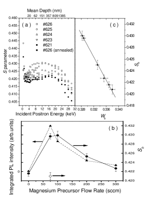
The PAS results are presented in Fig. 2(a). The parameters of the Mg-doped as-grown samples, along with those of the annealed sample and of the undoped reference sample, are shown as a function of positron implantation energy. The corresponding mean depths probed are also shown. For the undoped and the annealed samples, as the positron implantation energy increased, the parameters firstly decrease from the surface specific value (i.e., at low energy) and become approximately constant at around 0.420 above 2.5 keV, when almost all positrons are annihilated in the GaN film. The slight rise in parameters between 2.5 keV to 18 keV is consistent with a previous report Xiaodong02 which suggested that vacancies prefer to reside alongside dislocations, whose density increases towards the interface of the film and the nucleation layer. Beyond 18 keV, falls towards the value characteristic of the sapphire substrate (measured separately to be 0.392). Fig. 2(b) shows as a function of Mg concentration, where () is taken as the average of the () parameter measured in the energy range from 12 keV to 18 keV and represents the bulk film value. The highest values are observed for the most lightly-doped as-grown samples. With increasing Mg concentration, the value decreases and approaches those of the undoped and of the annealed samples. The dependence of on doping and annealing is very similar to that of the red luminescence (shown also in Fig. 2(b)) and of the ODMR signals detected in the red spectral region. This correlation thus provides strong support to the assertion that the red emission is associated with vacancy-type defects. Furthermore, the linear relationship between and shown in Fig. 2(c) is consistent with the existence of only one type of vacancy-related defect in the films R. Krause . The evidence points to the defects being related to the deep center signal in the ODMR spectra. In a separate ODMR experiment on the 2.8 eV “blue” band, the deeper donor signal () was obtained in both as-grown and annealed samples; therefore, it is unlikely that the donors account for the changes of the spectra.
We turn now to the identity of the deep vacancy-related center. Both Saarinen97 and Hautakangas03 have been observed in GaN by PAS. would be expected to be negatively charged and thus to act as a positron trap. CalculationsMattila97 ; Van de Walle94 have shown that the formation energy of is increased as the Fermi level moves towards the valence band. This result can be used to explain the decrease of strength of the red emission with Mg doping and annealing, for the reason that the concentration of decreases. To be observed in the ODMR spectrum, the vacancy would be expected to contain an odd number of holes in the optically-excited magnetic state and thus to be or (in the Sonder-SibleySonder notation, we write these as and respectively). The -value would be expected to be close to 2.00. It is also possible that the deep center is formed from an association between a Ga vacancy and an oxygen ion Reshchikov02 .
However, dominates over in Mg-doped GaN grown via MOVPE Hautakangas03 . If this complex forms the present deep center, the PAS results require it to be neutral or negatively charged (in order to trap the positrons). The neutral state, in the Sonder-Sibley notation, can be written as , where we have assumed the electron to be trapped in the vacancy. Under optical excitation the complex may lose an electron and become paramagnetic, leading again to an ODMR signal close to 2.00. It has been reported that the complex dissociates under -type conditions Hautakangas03 and therefore, with Mg doping and annealing, its concentration would be expected to decrease, leading to the decrease of the parameter and the red emission.

There are thus two possible models for the deep center, one involving gallium vacancies and the other nitrogen vacancy complexes. A one-electron energy level diagram which summarizes the conclusions is shown in Fig. 3. The diagram is similar to those in Refs. Kaufmann99 and Bayerl01 , except that the difference in the energies of the EM and deeper donor states in our case needs to be much smaller than the 250 meV proposed in the former reference (this is since, in our case, the emission bands involving either the EM and or the deeper donors both lead to red emission). If we take the MM1 center to be Ga vacancy-related center, the scheme of Fig. 3 is in agreement with that shown in Fig. 5 of Ref. Bayerl01 (but in contrast to the assignment in Ref. Hofmann00 ). Fig. 3 is almost certainly oversimplified and should be viewed with caution, since energy levels other than those shown are likely to be present. Further, there is strong evidence that the depth of the shallow acceptors (presumed to be formed by substitutional magnesium at gallium sites) is affected by Jahn-Teller effects and by the influence of strain and other nearby defects Aliev05 , so that it is represented in the diagram by a range of energy levels.
In summary, epitaxial GaN layers have been studied using ODMR and PAS. We find that the change of the PAS parameter with Mg concentration and annealing is correlated with the behavior of the PL and ODMR signals in the red region, indicating that the red luminescence is vacancy-related. The experiments lead to the conclusion that the red emission is due to recombination between electrons both from EM and from deeper donors with deep centers and point to the deep centers being vacancy-related defects.
We are grateful for support from the EPSRC (project GR/R34066) and for scholarships from Universities UK (SZ) and the State of Qatar (DAA). We thank R.J. Lynch for temperature treatment of the samples, S. Stepanov for Hall-effect measurements and X. D. Pi for valuable discussions.
References
- (1)
- (2)