Current address: ]IMEC, 3000 Leuven, Belgium
Electrical Detection of Spin Accumulation at a Ferromagnet-Semiconductor Interface
Abstract
We show that the accumulation of spin-polarized electrons at a forward-biased Schottky tunnel barrier between Fe and -GaAs can be detected electrically. The spin accumulation leads to an additional voltage drop across the barrier that is suppressed by a small transverse magnetic field, which depolarizes the spins in the semiconductor. The dependence of the electrical accumulation signal on magnetic field, bias current, and temperature is in good agreement with the predictions of a drift-diffusion model for spin-polarized transport.
pacs:
72.25.Dc,72.25.Mk,85.75.-dThe injection and detection of spin-polarized electrons in semiconductors are two of the important problems in the physics of spin transport. Recent experiments have demonstrated that it is possible to maintain a non-equilibrium spin polarization greater than 25% in a semiconductor by injection of electrons from a ferromagnetic metal through a tunnel barrier Hanbicki:2003 ; IBM:2005 ; Adelmann:2005 . In the case of a Schottky barrier, spin accumulation also occurs when electrons flow from the semiconductor to the ferromagnet Epstein:2003 ; Stephens:2004 ; Crooker:2005 . In almost all cases, however, measuring the spin polarization in the semiconductor has required the use of optical techniques. This raises the important question of whether an electrically generated spin polarization at a ferromagnet-semiconductor interface can also be detected electrically. The strongest test of any electrical spin detection measurement is the existence of a Hanle effect Johnson:1985 ; Jedema:2002 , in which spin accumulation is suppressed by precession in a transverse magnetic field. A Hanle effect has not been observed in electrical measurements of spin accumulation in semiconductors reported previously Hammar:2002 ; FertGaMnAs:2003 ; Schmidt:2001 . In contrast, the optical Hanle effect has served as the basis for a series of definitive measurements of spin-dependent phenomena in semiconductorsOpticalOrientation ; Kato:2004 .
In this Letter, we report a direct electrical transport measurement of spin accumulation at an Fe/-GaAs interface in the presence of a forward-bias current. The existence of a spin accumulation is established using the electrical Hanle effect Johnson:1985 . The spin-dependent voltage across the interface is suppressed by precession in a magnetic field applied perpendicular to the direction of spin polarization. The resulting peak in the voltage at zero magnetic field has a width determined by the timescales for spin precession, relaxation, drift, and diffusion. There is no corresponding electrical signature of spin injection under reverse bias, in agreement with a density of states argument based on tunnelling.
The samples are grown on semi-insulating GaAs (100) substrates. The lower part of the structure is composed of a 300 nm undoped GaAs buffer layer, followed by 2500 nm of Si-doped -GaAs ( cm-3), which forms the channel of the device. The junction region consists of a 15 nm GaAs transition layer followed by 15 nm (5 1018 cm-3) GaAs Hanbicki:2003 . The Fe film, 5 nm thick, is then deposited epitaxially at ∘C, followed by a 2 nm Al capping layer. A Schottky tunnel barrier is formed by the Fe and the highly doped GaAs layer. Samples with other channel doping levels were also prepared, as well as a control sample with the Fe film replaced with Al. The heterostructures are processed into Hall bars in which the heavily doped GaAs layer at the top of the structure is removed everywhere except underneath the Fe contacts. A photomicrograph of a typical device is shown in Fig. 1(a). The six Fe contacts are labelled a - e. The source and drain contacts a and b are separated by 150 m, which is much longer than the spin diffusion length ( m at 10 K) and spin drift length ( m at 10 K and 1.0 mA). The easy magnetization axis of each m Fe contact is parallel to the channel, which is along the GaAs [011] direction.
The calculated band diagram of the Fe/GaAs Schottky contacts is shown in Fig. 1(b) for three bias voltages covering the range of our experiment. Experimental I-V curves at K are shown in the inset. In addition to the voltage measured from the source (reverse-biased) to the drain (forward-biased), we also measure the other voltages indicated in Fig. 1(a). This approach allows us to determine the voltage drops at the source and drain contacts independently.
The lateral geometry allows us to image the spin polarization in the GaAs channel near the source and drain contacts using the magneto-optical Kerr effect. We follow the approach of Ref. Crooker:2005, to verify that an electron spin polarization exists at both the source and drain electrodes in the presence of a current. The polarization near the source electrode is due to spin injection through the Schottky barrier Zhu:2001 ; Hanbicki:2003 ; Adelmann:2005 , while the spin accumulation at the drain electrode is due to the spin-dependent reflectivity of the barrier under forward bias Epstein:2003 ; Stephens:2004 ; Ciuti . In either case, the polarization in the semiconductor is oriented antiparallel to the magnetization of the Fe contact Crooker:2005 and is suppressed by applying a magnetic field of 100 Oe perpendicular to the magnetization axis, demonstrating the existence of a Hanle effect.
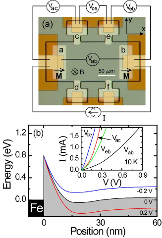
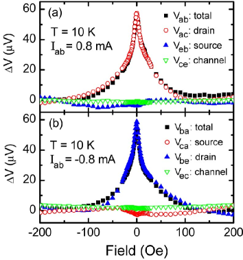
Given the existence of non-equilibrium spin populations at the source and drain, we consider the electrical transport properties of the device when a small magnetic field () is applied perpendicular to the plane of the structure. In this geometry, the magnetization of each electrode remains fixed during the measurement. Fig. 2(a) shows voltage measurements at 10 K for a 0.8 mA bias current flowing from contact to , so that electrons are flowing from (source) to (drain). The total source-drain voltage drop is approximately 0.5 V. A constant offset is subtracted from each curve, and a linear slope due to the Hall effect has also been removed from the data for and . The important feature of Fig. 2(a) is the peak at zero field in the total voltage as well as the drain voltage . These two measurements nearly coincide and have an amplitude V and full-width at half maximum (FWHM) 40 Oe. In contrast, no peak is observed in the source and channel voltages and . When the current direction in the channel is reversed, as for the data shown in Fig. 2(b), the peak is observed only for the voltage measurements that include contact , which is now the drain. The amplitude and FWHM of the peak are the same as in Fig. 2(a).
The asymmetry between source and drain shown in Fig. 2 has been observed in every Fe/GaAs device of this design that we have studied over the channel doping range from cm-3 to cm-3. No peak is observed in devices in which the Fe has been replaced by Al. Since the the electrode magnetization remains fixed, stray magnetic fields or anisotropic magnetoresistance can be excluded as possible origins of the effect. This conclusion is reinforced by the fact that the additional voltage drop is present only at the drain contact.
The voltage peak at zero field observed at the drain contact is a signature of spin accumulation at the ferromagnet-semiconductor interface. The effective resistance of the Schottky barrier is higher when a spin accumulation in the semiconductor is present. This is consistent with the model of Ciuti et al.Ciuti , in which the barrier is less transmissive for the spin state that accumulates in the semiconductor. The accumulation is suppressed by precession of the spin in a transverse field, leading to a decrease in the voltage. This explanation is also consistent with information inferred from the optical detection experiments Crooker:2005 , with which a more detailed comparison will be made below. As noted above, however, a non-equilibrium spin polarization is detected optically at both the source and drain electrodes, but the zero-field peak in the voltage is observed only at the drain contact. This reflects the fact that the Fe/GaAs interface acts as a tunnel barrier. At the reverse-biased source contact, the injected electrons tunnel from filled states in the ferromagnet into empty states in the semiconductor. These states are at an energy above the quasi-Fermi level for each spin, where is the voltage drop across the source contact. The fractional occupancy of these states is therefore small, and so the number of available states for each spin is essentially the same. As a result, the tunnelling resistance under reverse bias does not depend on the spin polarization in the semiconductor. The situation at the forward-biased drain contact is very different, since both the filled states in the semiconductor and the empty states in the ferromagnet have significant polarizations. In this case, the tunnelling current should be sensitive to the spin polarization in the semiconductor, as is observed experimentally.
Measurements of for different temperatures at a fixed bias current of 1.0 mA are shown in Fig. 3(a). To model these data, we adopt an approach used previously for spin-dependent transport in metals Johnson:1985 ; Jedema:2002 , but in this case the spins are generated and detected at a single ferromagnetic contact (the drain). We assume a mechanism in which the electrons in GaAs are polarized with an orientation along the magnetization axis by scattering from the interface at a point Ciuti . This process creates spin polarization at a rate per unit contact length. The spins then drift and diffuse under the contact before being detected at some time at another position . As the spins diffuse, they also precess about the applied field and decay with a relaxation time . The -component of the steady-state spin polarization at due to spin generated at is obtained by integrating the Green’s function solution of the drift-diffusion equation (including the spin relaxation and precession terms) over time, so that Johnson:1985 ; Jedema:2002 ; Stephens:2004 ; Crooker:2005
| (1) | |||||
where is the diffusion constant, is the drift velocity, is the -factor for electrons in GaAs, and is the Bohr magneton. The average spin polarization is determined by integrating over and , which vary from 0 to where m is the length of the drain contact.
With the exception of , the parameters in Eq. 1 are determined at each temperature by independent measurements. The drift velocity is calculated from the current using the carrier density determined from Hall measurements. The spin diffusion constant is determined from the measured Hall mobility, accounting for the temperature dependence of the Fermi distribution function at this densityFlatte:2000 . The spin lifetime is determined by the optical Hanle effect as measured by Kerr rotation. We assume that the voltage drop at the drain is proportional to and fit the data of Fig. 3(a) to the expected form of with (effectively the amplitude of the peak) as the only free parameter.
This procedure produces good agreement with the data at high temperatures, but the widths of the modelled peaks at low temperature are too small, with a discrepancy of approximately a factor of two at 10 K. This reflects a greater sensitivity of the model at low temperatures to the time for the electrons to drift across the contact. In practice, the current through the interface will be concentrated near the upstream edge of the contact and will be smallest near the downstream edge, with a gradient determined by the resistances of the channel and the interface, which are comparable [see inset of Fig. 1(b)]. We account for this by integrating over an effective length that is adjusted to fit one set of data (at 10 K) and then fixed for all other data sets. The solid curves in Fig. 3(a) are calculated using m.
An important aspect of the data that is predicted by the model is the increase in the FWHM of the peak as increases above 30 K. This is due to the temperature dependence of Kikkawa:1998 , which decreases in this sample from 45 nsec at 10 K to 5 nsec at 60 K. The peaks continue to broaden and decrease in amplitude above 60 K, but they can no longer be resolved above 80 K.
We can also show that the field dependence of the spin polarization that we measure electrically is the same as that measured by more traditional optical methods. To demonstrate this, a small magnetic field is applied in the plane of the sample (perpendicular to the magnetization), and the spin polarization is measured using Kerr microscopy Crooker:2005 . Electrically injected spins precess into the -direction, leading to a Kerr rotation proportional to . Fig. 3(b) shows measured at the edge of the source contact at three different temperatures. The solid curves are generated using the same parameters as for the transport data of Fig. 3(a) (except for the amplitude), with Eq. 1 modified to account for the fact that is sensitive to rather than . In this case, we integrate only over the source coordinate because is measured at a single point. The agreement with experiment is very good, providing extremely strong support for the interpretation of the transport measurements.
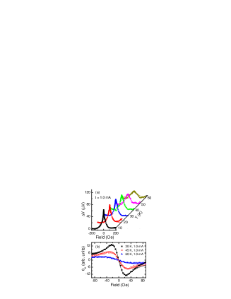
Besides , the other timescales that can determine the FWHM of the voltage peak are , , and . These have little effect at high temperature because they are all much larger than . At low temperatures, however, the two timescales that depend on become shorter than at the highest bias currents. The source-drain voltage is shown for several different bias currents at 10 K in Fig. 4(a). The solid curves are generated from the model with m.
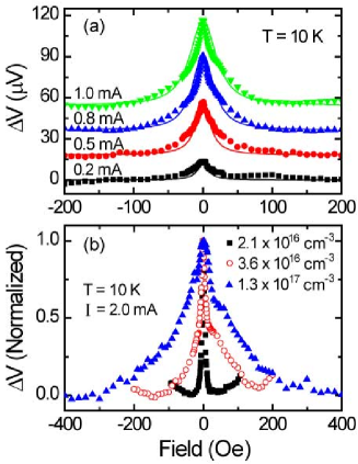
The amplitude, which is the only other parameter, is nearly proportional to the current. The FWHM of the model curves also increases with current, due primarily to the fact that decreases from 130 nsec at 0.2 mA to 20 nsec at 1.0 mA. The limiting width at small bias is set by spin relaxation ( nsec at 10 K) and diffusion.
The width also increases with bias current in the experimental data. At the highest currents, however, the peaks become sharper in the region Oe. This can be seen more prominently in Fig. 4(b), which shows at a current of 2.0 mA for this sample ( cm-3) and two others with different channel dopings. The narrow features near zero field become stronger with decreasing doping and are characteristic of an enhancement of the effective magnetic field acting on the electrons due to dynamic polarization of nuclei DNP . This effect is regularly observed in optical pumping experiments and is also seen in optical measurements of the spin accumulation under forward bias Epstein:2003 ; Stephens:2004 . Excluding very small fields, Fig. 4(b) shows an overall correlation between the FWHM and doping that is expected given the dependence of on carrier density Kikkawa:1998 ; Dzhioev:2002 . For example, the highest FWHM is observed for the sample with the largest channel doping ( cm-3).
The measurements discussed here show that the electrically generated spin accumulation at a forward-biased -GaAs/Fe Schottky contact can also be detected electrically. A quantitative comparison is made with the established approach of optical detection. The results demonstrate that it is possible to determine important parameters of a semiconductor spin transport device using electrical measurements alone.
This work was supported by the DARPA SpinS and Los Alamos LDRD programs, the NSF MRSEC program under DMR 02-12032, ONR, and the NSF NNIN program through the Minnesota Nanofabrication Center.
References
- (1) A. T. Hanbicki et al., Appl. Phys. Lett. 82, 4092 (2003).
- (2) X. Jiang et al., Phys. Rev. Lett. 94, 056601 (2005).
- (3) C. Adelmann et al., Phys. Rev. B 71, 121301(R) (2005).
- (4) R. J. Epstein et al., Phys. Rev. B 68, 041305(R) (2003) showed an enhancement of effects observed earlier with no bias current: R. K. Kawakami et al., Science 294, 131 (2001); R. J. Epstein et al., Phys. Rev. B 65, 121202(R) (2002).
- (5) J. Stephens et al., Phys. Rev. Lett. 93, 097602 (2004).
- (6) S. A. Crooker et al., Science 309, 2191 (2005).
- (7) M. Johnson and R. H. Silsbee, Phys. Rev. Lett. 55, 1790 (1985); Phys. Rev. B 37, 5326 (1988).
- (8) F. J. Jedema et al., Nature 416, 713 (2002).
- (9) P. R. Hammar, B. R. Bennett, M. J. Yang, and M. Johnson, Phys. Rev. Lett. 83, 203 (1999); P. R. Hammar and M. Johnson, Phys. Rev. Lett. 88, 066806 (2002).
- (10) R. Mattana et al., Phys. Rev. Lett. 90 166601(2003).
- (11) G. Schmidt et al., Phys. Rev. Lett. 87, 227203 (2001).
- (12) Optical Orientation, edited by F. Meier and B. P. Zakharchenya (North-Holland, Amsterdam, 1984).
- (13) A recent example is the demonstration of the spin Hall effect: Y. K. Kato, R. C. Myers, A. C. Gossard, and D. D. Awschalom, Science 306, 1910 (2004).
- (14) H.J. Zhu et al., Phys. Rev. Lett. 87, 016601 (2001).
- (15) C. Ciuti, J. P. McGuire, and L. J. Sham, Phys. Rev. Lett. 89, 156601 (2002); J. P. McGuire, C. Ciuti, and L. J. Sham, Phys. Rev. B 69 115339 (2004). For other approaches, see V. V. Osipov and A. M. Bratkovsky, Phys. Rev. B 72, 115322 (2005); G. E. W. Bauer et al., Phys. Rev. B 72, 155304 (2005).
- (16) M. E. Flatté and J. M. Byers, Phys. Rev. Lett. 84, 4220 (2000).
- (17) J. M. Kikkawa and D. D. Awschalom, Phys. Rev. Lett. 80, 4313 (1998).
- (18) V. G. Fleisher and I. A. Merkulov, in Ref. OpticalOrientation, . The dynamic polarization is due to a small () misalignment of our sample.
- (19) R. I. Dzhioev et al., Phys. Rev. B 66, 245204 (2002).