Conductance in strongly correlated 1D systems: Real-Time Dynamics in DMRG
Abstract
A new method to perform linear and finite bias conductance calculations in one dimensional systems based on the calculation of real time evolution within the Density Matrix Renormalization Group (DMRG) is presented. We consider a system of spinless fermions consisting of an extended interacting nanostructure attached to non-interacting leads. Results for the linear and finite bias conductance through a seven site structure with weak and strong nearest-neighbor interactions are presented. Comparison with exact diagonalization results in the non-interacting limit serve as verification of the accuracy of our approach. Our results show that interaction effects lead to an energy dependent self energy in the differential conductance.
pacs:
73.63.-b, 72.10.Bg, 71.27.+a, 73.63.KvDuring the past decade improved experimental techniques have made production of and measurements on one-dimensional systems possible Sohn et al. (1997), and hence led to an increasing theoretical interest in these systems. However, the description of non-equilibrium transport properties, like the finite bias conductance of an interacting nanostructure attached to leads, is a challenging task. For non-interacting particles, the conductance can be extracted from the transmission of the single particle levels Landauer (1957, 1970); Büttiker (1986). Since the screening of electrons is reduced by reducing the size of structures under investigation, electron-electron correlations can no longer be neglected. Recently several methods to calculate the zero bias conductance of strongly interacting nanostructures have been developed. One class of approaches consists in extracting the conductance from an easier to calculate equilibrium quantity, e.g. the conductance can be extracted from a persistent current calculation Molina et al. (2004), from phase shifts in NRG calculations Oguri et al. (2005), or from approximative schemes based on the tunneling density of states Meir et al. (1991). Alternatively one can evaluate the Kubo formula within Monte-Carlo simulations Louis and Gros (2003), or from DMRG calculations Bohr et al. (2006). In contrast, there are no general methods available to get rigorous results for the finite bias conductance. While the problem has been formally solved by Meir and Wingreen using Keldysh Greens functions Meir and Wingreen (1992), the evaluation of these formulas for interacting systems is generally based on approximative schemes.
In this work we propose a new concept of calculating finite bias conductance of nanostructures based on real time simulations within the framework of the DMRG White (1992, 1993); Cazalilla and Marston (2002); Luo et al. (2003); Daley et al. (2004); White and Feiguin (2004); Schmitteckert (2004); Feiguin and White (2005). It provides a unified description of strong and weak interactions and works in the linear and finite bias regime, as long as finite size effects are treated properly.
In a first approach of real time dynamics within DMRG, Cazalilla and Marston integrated the time-dependent Schrödinger equation in the Hilbert space obtained in a finite lattice ground state DMRG calculation Cazalilla and Marston (2002). Since this approach does not include the density matrix for the time evolved states, its applicability is very limited. Luo, Xiang and Wang Luo et al. (2003) improved the method by extending the density matrix with the contributions of the wave function at intermediate time steps. Schmitteckert Schmitteckert (2004) showed that the calculations can be considerably improved by replacing the integration of the time dependent Schrödinger equation with the evaluation of the time evolution operator using a Krylov subspace method for matrix exponentials and by using the full finite lattice algorithm.
An alternative approach is based on the wave function prediction White (1996). There one first calculates an initial state with a static DMRG. One iteratively evolves this state by combining the wave function prediction with a time evolution scheme. In contrast to the above mentioned full t-DMRG, one keeps only the wave functions at two time steps in each DMRG step. In current implementations the time evolution is calculated by approximative schemes, like the Trotter decomposition Daley et al. (2004); White and Feiguin (2004), or the Runge-Kutta method Feiguin and White (2005). In our work, we combined the idea of the adaptive DMRG method with direct evaluation of the time evolution operator via a matrix exponential as described in Ref. Schmitteckert (2004). Therefore our method involves no Trotter approximations, the time evolution is unitary by construction, and it can be applied to models beyond nearest-neighbor hopping.
The Hamiltonian for the nanostructure attached to leads, is given by
| (1a) | |||||
| (1b) | |||||
| (1c) | |||||
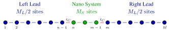
Individual sites are labeled according to Fig. 1, is the size of the interacting nanostructure, denotes a local external potential, which can be applied to the nanostructure, and is a nearest-neighbor interaction term inside the nanostructure. The hopping elements in the leads, the structure, and coupling of the structure to the leads are , , and respectively.

Similar to the approach in Schmitteckert (2004) we add an external source-drain potential to the unperturbed Hamiltonian and take the ground state of , obtained by a standard finite lattice DMRG calculation, as initial state at time Schmitteckert (2004). In addition we target for the ground state of . In actual calculations the switched external potential was smeared out over three lattice sites.
We then perform a time evolution as described above by applying the time evolution operator on 111It is equally possible to prepare the system in the groundstate of the Hamiltonian , and to perform the time evolution via . 222We use a time step of . In each adaptive time step one intermediate time step is targeted and 2 sweeps are performed., which leads to flow of the extended wave packet through the whole system until it is reflected at the hard wall boundaries as described in Schmitteckert (2004).
The expectation value of the current at each bond and every time step is given by
| (2) |
Following Refs. Wingreen et al. (1993); Cazalilla and Marston (2002) we define the current through the nanostructure as an average over the current in the left and right contacts to the nanostructure
| (3) |
For the calculation of the DC-conductance through the nanostructure the time evolution has to be carried out for sufficiently long times until a quasi-stationary state is reached and the steady state current can be calculated. If the stationary state corresponds to a well-defined applied external potential , the differential conductance is given by In the limit of a small applied potential, , the linear conductance is given by
We first consider the transport through a single impurity.
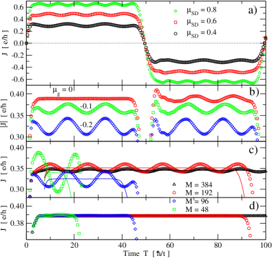
The current rises from zero and settles into an oscillating quasi-stationary state (Fig. 2). After the wavepackets have travelled to the boundaries of the system and back to the nanostructure, the current falls back to zero and changes sign. The amplitudes of the oscillations depend on and , and are proportional to the inverse of the system size . The period of oscillation strongly depends on the applied potential [Fig. 2 (a)] but is independent of the gate potential and system size [Fig. 2 (b), (c)], and is given by . This periodic contribution to the current is reminiscent of the Josephson contribution in the tunneling Hamiltonian, obtained by gauge transforming the voltage into a time dependent coupling . It is present even for zero gate potential, but the currents in the left and right leads oscillate with opposite phase and cancel in the current average Eq. (3). After the wavepackets have finished one round trip, the current oscillations reappear because of the additional phase shift due to the different lengths of the left and right leads [Fig. 2 (b)].

The stationary current is given by a straightforward average, because the oscillation period is known. In general, the density in the leads, and therefore also the current, depends on the system size and a finite size analysis has to be carried out in order to extract quantitative results [Fig. 2 (c), see also discussion of Fig. 6]. Only in special cases (symmetry, half filled leads, and zero gate potential) is the stationary current independent of the system size [Fig. 2 (d)].
Our result for the conductance through a single impurity in Fig. 3 is in excellent quantitative agreement with exact diagonalization results already for moderate system sizes and DMRG cutoffs. Accurate calculations for extended systems with interactions are more difficult, mainly for two reasons: 1.) The numerical effort required for our approach depends crucially on the time to reach a quasi-stationary state. For the single impurity, the quasi-stationary state is reached on a timescale proportional to the inverse of the width of the conductance resonance, , in agreement with the result in Ref. Wingreen et al. (1993). In general, extended structures with interactions will take longer to reach a quasi-stationary state, and the time evolution has to be carried out to correspondingly longer times. 2.) In the adaptive t-DMRG, the truncation error grows exponentially due to the continued application of the wave function projection, and causes the sudden onset of an exponentially growing error in the calculated time evolution after some time. This ’runaway’ time is strongly dependent on the DMRG cutoff, and was first observed in an adaptive t-DMRG study of spin transport by Gobert et al.Gobert et al. (2005). We observe the sudden onset of an exponentially growing error in our calculations as well, Fig. 4, but in addition to the dependence on , the ’runaway’ time now also depends strongly on . To avoid these problems one has to resort to the full t-DMRG Schmitteckert (2004), which does not suffer from the runaway error. A detailed analysis of the numerics of our approach will be published elsewhere 333G. Schneider and P. Schmitteckert, to be published..
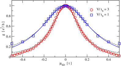
In Fig. 5 we show results for the first differential conductance peak of an interacting 7-site nanostructure. Careful analysis of the data shows, that in order to reproduce the line shape accurately, one has to introduce an energy dependent self energy. Since the effect is small, we approximate it by a correction quadratic in the bias voltage difference . It is important to note that for the strongly interacting nanostructure, , the conductance peaks are very well separated. Therefore the line shape is not overlapped by the neighboring peaks, and the fit is very robust. Performing the same analysis for a non-interacting nanostructure with a comparable resonance width, we obtain negligible corrections to in the self energy, indicating that the change of the line shape is due to correlation effects.
The linear conductance as a function of applied gate potential can be calculated in the same manner, if a sufficiently small applied external potential is used. We study the same non-interacting 7-site nanostructure as before and use a bias voltage of .
For half filled leads, the result for the linear conductance calculated with a fixed number of fermions, , is qualitatively correct, but the conductance peaks are shifted to higher energies relative to the expected peak positions at the energy levels of the non-interacting system (Fig. 6). Varying the gate potential increases the charge on the nanostructure by unity whenever an energy level of the nanostructure moves through the Fermi level [Fig. 6 (b)]. The density in the leads varies accordingly [Fig. 6 (c)]. Since the number of fermions in the system is restricted to integer values, direct calculation of the linear conductance at constant is not possible and one must resort to interpolation. Using linear interpolation in for yields our final result for the linear conductance at half filling [Fig. 6 (a)]. The agreement in the peak positions is well within the expected accuracy for a 96 site calculation.
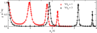
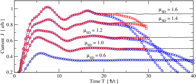
Our results for the conductance through an interacting extended nanostructure are presented in Fig. 7. The calculation for the weakly interacting system requires roughly the same numerical effort as the non-interacting system. In the strongly interacting case, where the nanostructure is now in the charge density wave regime, the time to reach a quasi-stationary state is longer, and a correspondingly larger system size was used in the calculation. In both cases we obtain peak heights for the central and first conductance resonance to within 1% of the conductance for a single channel.
We have introduced a new concept of extracting the finite bias and linear conductance from real time evolution calculations. Very accurate quantitative results are possible, as long as finite size effects are taken into account. Our results for the linear conductance compare favorably both in accuracy and computational effort with the DMRG evaluation of the Kubo formula Bohr et al. (2006). Calculations of strongly interacting systems show correlation induced corrections to the resonance line shape.
We profited from many discussions with Peter Wölfle. The authors acknowledge the support from the DFG through project B2.10 of the Center for Functional Nanostructures, and from the Landesstiftung Baden-Württemberg under project B710.
References
- Sohn et al. (1997) L. L. Sohn, L. P. Kouwenhoven, and G. Schön, eds., Mesoscopic electron transport: Proceedings of the NATO Advanced Study Institute (1997).
- Landauer (1957) R. Landauer, J. Res. Dev. 1, 233 (1957).
- Landauer (1970) R. Landauer, Phil. Mag. 57, 863 (1970).
- Büttiker (1986) M. Büttiker, Phys. Rev. Lett. 57, 1761 (1986).
- Molina et al. (2004) R. A. Molina et al., Eur. Phys. Jour. B 39, 107 (2004).
- Oguri et al. (2005) A. Oguri, Y. Nisikawa, and A. C. Hewson, .Phys. Soc. Jpn. 74, 2554 (2005).
- Meir et al. (1991) Y. Meir, N. S. Wingreen, and P. A. Lee, Phys. Rev. Lett 66, 3048 (1991).
- Louis and Gros (2003) K. Louis and C. Gros, Phys. Rev. B 68, 184424 (2003).
- Bohr et al. (2006) D. Bohr, P. Schmitteckert, and P. Wölfle, Europhys. Lett. 73, 246 (2006).
- Meir and Wingreen (1992) Y. Meir and N. S. Wingreen, Phys. Rev. Lett 68, 2512 (1992).
- White (1992) S. R. White, Phys. Rev. Lett. 69, 2863 (1992).
- White (1993) S. R. White, Phys. Rev. B 48, 10345 (1993).
- Cazalilla and Marston (2002) M. A. Cazalilla and J. B. Marston, Phys. Rev. Lett. 88, 256403 (2002).
- Luo et al. (2003) H. G. Luo, T. Xiang, and X. Q. Wang, Phys. Rev. Lett. 91, 049701 (2003).
- Daley et al. (2004) A. J. Daley et al., J. Stat. Mech.: Theor. Exp. p. P04005 (2004).
- White and Feiguin (2004) S. R. White and A. E. Feiguin, Phys. Rev. Lett. 93, 076401 (2004).
- Schmitteckert (2004) P. Schmitteckert, Phys. Rev. B 70, R121302 (2004).
- Feiguin and White (2005) A. E. Feiguin and S. R. White, Phys. Rev. B 72, 020404(R) (2005).
- White (1996) S. R. White, Phys. Rev. Lett 77, 3633 (1996).
- Wingreen et al. (1993) N. S. Wingreen, A. P. Jauho, and Y. Meir, Phys. Rev. B 48, 8487 (1993).
- Gobert et al. (2005) D. Gobert et al., Phys. Rev. E 71, 036102 (2005).