Electronic Control and Readout of Qubit States in Solid State Quantum Computing Systems
Abstract
We demonstrate that an junction is the most suitable candidate for electronic control and readout of qubit states in quantum computing systems based on shallow impurities. The signature of this system is that the regions serve as metallic electrodes separated form the region by a self-induced barrier (internal workfunction). The system mimics the properties of a metal-vacuum-metal junction with the qubit (impurity atom) placed in a “vacuum” -region between two “metallic” electrodes. We will show that the self-induced barrier exists in a sufficiently wide range of the concentration of dopants in the -semiconductor (e.g. up to cm-3 for Si) and its height can be controlled by tuning the doping level. A shallow donor placed in a vacuum -region will be populated with one electron in equilibrium. In the case of Li donor in Si the -electrodes will be used for a precision placement of the Li atom during the growth process; for voltage control and manipulation of the qubit states; and for a qubit readout by means of the optically stimulated resonant tunnelling. Another important feature of our system is that the qubit states (first two lowest energy levels of Li in Si) are separated by an energy gap from a continuum of the many-body states of the controlling electrodes.
pacs:
68.65.Hb, 03.67.Pp, 03.67.Lx, 63.20.KrIntroduction. Various systems have been proposed during last decade as potential candidates for solid state quantum computing (QC). All these systems are based on control of either localized spins or localized charged states in semiconductors. In particular, it was proposed to encode qubits on: nuclear spins of 31P donors Kane (1998); Skinner et al. (2003) or 29Si isotopes Ladd et al. (2002) in Si matrix; spins of electrons localized in semiconductor quantum dots (QDs) Loss and DiVincenzo (1998); Imamoglu et al. (1999); Vrijen et al. (2000); Sherwin et al. (1999); Chen et al. (2000); Stievater et al. (2001); Brown et al. (2002); and on charged states of shallow impurities in Si Golding and Dykman ; Smelyanskiy et al. (2005). For all these cases the distance between neighboring qubits ranges from 5nm Kane (1998); Skinner et al. (2003); Ladd et al. (2002) to 100nm Golding and Dykman ; Smelyanskiy et al. (2005) and electronic control must be used for a readout and for one- and two-qubit gates. It is clear, that the distance between an individual qubit and its controlling electrode has to be smaller than the interqubit separation to ensure a proper space resolution of the qubits. Thus the distance must be in the range 5nm (nuclear spins Kane (1998); Skinner et al. (2003); Ladd et al. (2002)) and 20nm (shallow impurities in Si Smelyanskiy et al. (2005); Golding and Dykman ).
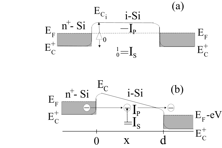
It seems almost obvious that one can use metal electrodes for control and readout of the solid state qubits. As it has been suggested in most of the solid state QC proposals Kane (1998); Skinner et al. (2003)-Golding and Dykman , the thin-film metal electrodes have to be deposited directly on a Si surface or on a thin insulating SiO2 layer grown on this surface. A careful analysis of this idea reveals that a single shallow donor in an undoped semiconductor placed in a proximity ( 5-20nm) of an interface with the metal will be ionized. It simply means that the qubit cannot be formed. This conclusion is in agreement with the fact the localized electrons on shallow impurities placed in vicinity of metal electrodes have not been observed in QC experiments. Indeed, it is well known that a high potential barrier (a Schottky barrier) is always formed at metal-semiconductor (MS) or metal-insulator-semiconductor (MIS) interfaces Sze (1981). The barrier height is determined by a large density of the interfacial states that pin the Fermi level at energy - eV below the conduction band edge at the interface. The pinning occurs for Si and GaAs in contacts with almost all metals and for doping concentrations cm-3 the barrier width is in the range nm Sze (1981). However an extremely pure (-)S layer with defect density cm-3 has to be used for the solid state QC. For these concentrations the barrier width is in the range of m or more, and inside -S layer the conduction band edge is practically constant at the distances to the interface corresponding to the qubit location, 20 nm. Therefore the potential of the -S layer between two control metal electrodes will be flat (see Fig. 1(a)). The barrier height is in the range 0.5-0.8 eV and all shallow donors with ionization energy 100 meV will be ionized.
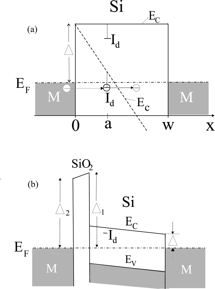
One can apply an electric field to push the impurity level below the Fermi energy of the left electrode (see Fig. 1(a)). However the required electric field, V/cm ( is the elementary charge), is so strong that the impurity will be ionized due to the Zener tunnelling breakdown into the right contact Sze (1981).
The potential barrier can be efficiently decreased if a very thin heavily doped -S layer with donor concentration cm-3 is formed between M and -S layers Sze (1981). The required conditions will be fulfilled if in -semiconductor layer at a distance (cf. Fig. 1(a)). Unfortunately, these extremely stringent conditions cannot be satisfied simultaneously for a sufficiently large interface plane and a sequence of donor qubits located near it, because of the large fluctuations of the Schottky barrier and the number of donors in the thin layer Das et al. (1989); Palm et al. (1993); Tung (1992); Zheng et al. (1999). Similar overwhelming obstacles also arise in MIS structures with thin insulating layers (Fig. 1(b)). We note that the barrier height at SiO2-Si interface is about 4 eV Sze (1981) and therefore it is impossible to push the donor level below with any realistic electric fields.
The purpose of this paper is to demonstrate that an junction is the most suitable candidate for electronic control and readout of qubit states in quantum computing systems based on shallow impurities. The signature of this system is that the regions serve as metallic electrodes separated form the region by a self-induced barrier (internal workfunction). The system mimics the properties of a metal-vacuum-metal junction with the qubit (impurity atom) placed in a “vacuum” -region between two “metallic” electrodes. As we will see below, the self-induced barrier exists in a sufficiently wide range of the concentration of dopants in the -semiconductor (e.g. up to cm-3 for Si) and its height can be controlled by tuning the doping level. A shallow donor placed in a vacuum -region will have its ground state energy below the Fermi level and will be populated with one electron in equilibrium.
Finally, we note that for a qubit based on Li donor in Si Smelyanskiy et al. (2005) the same -electrodes can be be used for a precision placement of the electro-migrating Li ions during the growth process; for voltage control and manipulation of the qubit states in Li at low temperatures; and for a qubit readout by means of the optically stimulated resonant tunnelling.
LDA treatment of doped semiconductor +-i structure. Let us consider formation of a barrier at a interface. We will assume that the donor concentration in -region exceeds the threshold of the metal-insulator phase transition. If we replace spatial distribution of ionized donors with positive uniform charge and consider a single-valley parabolic-band -type semiconductor (e.g. GaAs) the problem can be mapped onto the problem of a metal-vacuum interface Bardeen (1936); Smith (1969); Lang and Kohn (1971). The barrier of an junction or, equivalently, the workfunction of a simple metal can be expressed in the form known as Budd-Vannimenus theorem Budd and Vannimenus (1973); Mahan and Schaich (1974):
| (1) |
The meaning of Eq. (1) is illustrated in Fig. 2 where a schematic band diagram of the -junction is shown.
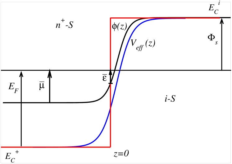
The energies and are the conduction band edges of and -semiconductors respectively, is the exact one-electron quasi-particle potential, and is the exact electrostatic (Hartree) energy of the electron related to the electron density through the Poisson’s equation:
| (2) |
where is a step function. The quantities and are the exact chemical potential many-body effects included Lang and Kohn (1971) and the exact total energy per one electron in the bulk respectively. All these quantities are well known within the local density approximation (LDA). In particular,
| (3) |
where we introduced the effective Rydberg:
| (4) |
is the dielectric constant, is the effective mass, and is the effective Bohr radius:
| (5) |
The parameter is related to the bulk electron concentration in the region as follows:
| (6) |
where is the donor concentration and we assume that all the donors are ionized, i.e. .
Since is known the problem of finding the barrier is reduced to calculation of the potential difference caused by the interfacial dipole layer. The latter can be expressed as:
| (7) |
where we introduced dimensionless energy , and coordinate . Here is the total number of electrons per unit area in the half-space , and
| (8) |
is a dimensionless effective density of the occupied states for electrons moving perpendicular to the interface.
Eq. (7) is exact and follows from the properties of the 1-dimensional Poisson’s equation. The internal workfunction can be calculated exactly provided that we know the eigenfunctions of the Kohn-Sham equations :
| (9) |
with
| (10) |
where , electrostatic energy is related to via Eq. (2), and
| (11) |
The detailed numerical solution of Eqs. (9)-(11) will be published elsewhere. Here we will estimate the interface dipole term using approximate eigenfunctions of the one-electron Schrodinger equation with the potential in the form of a rectangular step of the height (shown in red in Fig. 2):
| (12) |
where . The wavefunctions in Eq. (12) capture the most important feature of the exact solution - exponential asymptotic decay far from the interface Levy et al. (1984). An estimate for the value of the parameter can be obtained from the Thomas-Fermi equation inside -region (). This yields:
| (13) |
Substituting Eqs. (12) and (13) in Eq. (7) we obtain:
| (14) |
where
| (15) |
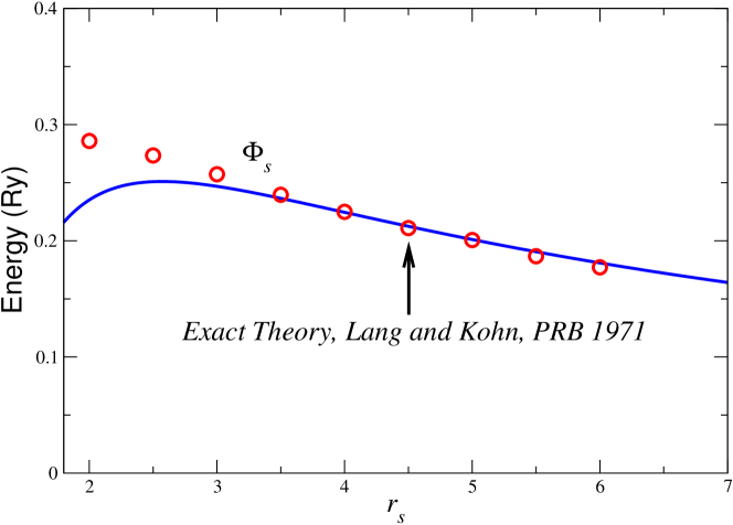
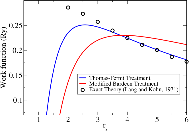
The results of the application of Eq. (14) are shown in Fig. 3 and compared with the exact numerical results by Lang and Kohn Lang and Kohn (1971). We see that our estimate is in good agreement with the exact theory for 2.5. As we will see below this region of electron densities is the most relevant one for quantum computing purposes in Si system.
In order to apply our results to Si we have to take into account multi-valley character of the kinetic energy operator. If we neglect the effective mass anisotropy the main effect will consist in replacing parameter with its renormalized value , where is the number of valleys in the conduction band. The analog of Eq. (14) reads:
| (16) |
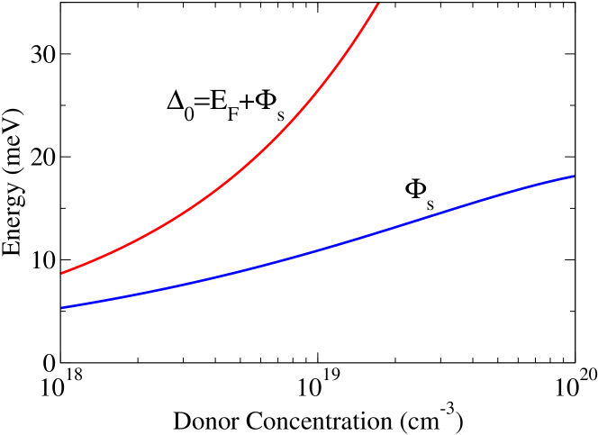
where the number of valleys =6 for Si. Here we have omitted insignificant correlation energy. The results of the calculations of by means of Eq. (16) are shown in Fig. 4 We used = 34.5 meV, and = 18.3 ÅPerera et al. (1995). It can be seen from Fig. 4 that for the purposes of quantum computing on long-lived donor states of Li in Si Smelyanskiy et al. (2005) the electron concentration in electrodes must be in the range between 2.551018 cm-3 () and 1.51019 cm-3 (). The lower limit is the metal-insulator transition threshold for Si Shklovskii and Efros (1984); Perera et al. (1995) while the upper limit corresponds to the point where the total conduction band offset between - and -layers reaches 1 Ry∗. A schematic energy diagram corresponding to this range of concentrations is shown in Fig. 5 (a). It can be seen that the first two lowest energy levels of Li donor in Si are separated by an energy gap from a continuum of the many-body states in the -electrodes. Thus our qubit is protected from a dephasing caused by dynamic fluctuations of the electron density in the contacts.
Qubit state readout via photo-assisted resonant tunnelling. The -- or -- structures can be used for readout the electron states in systems considered in Refs. Golding and Dykman ; Smelyanskiy et al. (2005). Indeed, and individual qubit in these systems is encoded on the ground and long-lived first excited state of a shallow donor or acceptor. According to estimates of Ref. Smelyanskiy et al. (2005) for one of those systems, Li donor in Si, the lifetime of the first excited state 1s,B2 (further denoted as ) can be up to 1 second if the energy separation between this state and the ground state 1s,A1 (further denoted as ) is 0.06 meV. The ionization energy of the ground state of Li in Si, =1 Ry∗=34.5 meV. The excited -state has the ionization energy =11.5meV and the lifetime 10-8s Pavlov et al. (2000). The readout can be realized when the lower levels and lie below and the -level is higher than (Fig. 5(b)). This situation corresponds to doping concentration cm-3. In this case the lower levels of the qubit lie below the continuum spectrum of the contacts in equilibrium and one of them is populated by the electron which does not interact with electrons in conducting layers (Fig. 5(b)). When bias voltage 30 meV is applied the -level moves down below the Fermi level of the left electrode and all Li levels are shifted under the action of electric field 4KV/cm (Fig. 5(c)). Radiation absorption between lower Li states or and the state 2p0 depends on the polarization of the infrared light. Thus, selecting the radiation by frequency and polarization we can excite only the state or depending on the polarization and detect the tunnelling current through the -level of the ionized impurity (Fig. 5(c)). The tunnelling frequency can be estimated as
where is the tunnelling length. For typical values =8meV, 20meV and =25nm we obtain 1010 Hz, i.e. . It means that many electrons will tunnel through the excited -level before the recombination process occurs, the donor becomes neutral, and the current terminates. Thus a single-qubit measurement with the current signal much stronger than that of the single-electron measurement can be realized. The tunnelling current depends dramatically on Li position, namely it has a sharp maximum when the Li atom is placed equidistantly between the electrodes Xu et al. (1995); Osipov et al. (2004). This effect can be used for in situ placement control of Li atoms during the growth process at high temperatures, when the highly-mobile Li ions are guided to their permanent final positions by an external electric field.
The effect of photo-stimulated resonant tunnelling can be verified independently in the experiments on -doped Li layers placed between two -electrodes. These structures are similar to those studied in Ref. Caro et al. (2003). Consider kinetics of the resonant current immediately after the photoionization occurs. For simplicity we assume that the tunnelling frequency is relatively small, , where is a total decoherence width of the 2 level. Then the rate equations for sequential resonant tunnelling read:
| (17) | |||||
| (18) |
Here are the populations of the levels and , , and are inverse elastic tunnelling lifetimes, and W is the inverse recombination time. The first term in Eq. (17) takes into account the Coulomb blockade effect. The difference between Eqs. (17), (18) and conventional equations Datta (1995) is that the resonant current is decaying via the recombination channel. If the population quickly attains quasi-equilibrium and the tunnelling current can be expressed as:
| (19) |
where
| (20) |
Therefore, the photo-stimulated resonant tunnelling current through the -doped Li layer will be characterized by a long-term decay kinetics . We note that the condition for the sequential tunnelling consider above is opposite to that required for the qubit readout. In the letter case and a coherent resonant tunnelling regime needs to be considered.
Conclusion We proposed a device based on heterostructures for electronic control and readout of qubit encoded in two lowest states of a shallow donor of Li in Si. Qubit state readout is based on the polarization-sensitive photo-stimulated resonant tunnelling effect. A key feature of the system is that the qubit states (first two lowest energy levels of a donor) are separated by a finite energy gap from a continuum of the many-body states of the controlling electrodes. Therefore the qubit is protected from a dephasing caused by dynamic fluctuations of the electron density in the contacts. It is of interest to apply the proposed scheme for the case of qubits based on orbital states of quantum dots as well as on shallow acceptor states Golding and Dykman (in the later case -- structures should be used).
Appendix A Thomas-Fermi equation
According to the Thomas-Fermi theory the electrons are considered as classical particles obeying Fermi statistics.Then the maximal energy of an electron near point reads:
| (21) |
where is the electrostatic (Hartree) energy of an electron in the field of all other electrons and external potential, is the magnitude of the elementary charge, is the electrostatic potential, and is the maximal momentum of the electron. The maximal energy of the electron is nothing but a chemical potential at . This chemical potential must be constant in equilibrium:
| (22) |
where
| (23) |
Here is the electron density in the bulk and is the concentration of donors. The maximal(Fermi) momentum can be related to the number density of the electrons :
| (24) |
Thus, from Eqs. (21)-(24) the relation between electron density and electrostatic energy within the Thomas-Fermi model is:
| (25) |
The Poisson equation for reads:
| (26) |
Introducing dimensionless energy , from Eqs (25)-(26) we obtain the self-consistent, dimensionless, Thomas-Fermi equation:
| (27) |
Here we introduced dimensionless length , where is the Thomas-Fermi screening length:
| (28) |
Here is the Bohr radius.
The equation can be solved as:
| (29) |
Therefore, we obtain:
| (30) |
It can be shown (Mahan and Schaich (1974)) that . Therefore the solution of the Thomas-Fermi equation for reads:
| (31) |
where . Finally, from Eqs. (25) and (31) we obtain for :
| (32) |
Integrating Eq. (32) from to we obtain the total number of electrons per unit area in the upper half-space (or holes in the lower half-space):
| (33) |
and the prefactor in the expression for :
| (34) |
Appendix B Electron Density
To calculate the electron density using LDA wavefunctions we have to take into account the fact that we are dealing with the wavefunction of a -semi-infinite metal:
| (36) |
The quantum number describes the bulk states, i.e. as . Using Eq. (36) we can calculate the number density:
| (37) | |||||
| (38) |
Introducing dimensionless energy we further obtain:
| (39) |
If we know we can normalize the wavefunctions in the upper half-space:
| (40) |
where
| (41) |
Appendix C 1D Poisson Equation
Appendix D Modified Bardeen Treatment.
J. Bardeen, in his pioneering work of 1936 Bardeen (1936), calculated a moment of a surface dipole layer using a model step-like potential barrier of infinite height. Her we will follow a similar path but assume that the height of the barrier is finite. The value of the barrier will be determined self-consistently.
Let us approxiamte the exact self-consistent potential of a semiinfinite jellium metal with a step function:
| (45) |
Here, as previously, , and we assumed that the region of the classical motion of electrons is extended beyond the metal surface . This assumption is necessary to ensure elelctroneutrality of the system. Integrating the charge densities inside and outside the metal and imposing the electroneutrality condition we find :
| (46) |
where
| (47) | |||||
| (48) |
The limiting value was previously found by Bardeen Bardeen (1936) (see also Ref. Newns (1970)).
As a next step we integrate the Poisson’s equation and employ Eq. (1) to determine self-consistently. This leads to a transcendental equation similar to Eq. (14):
| (50) |
where
| (51) |
and
| (52) |
The value of obtained from Eq. (50) is shown in Fig. 6 and compared with our previous Thomas-Fermi result. We see that the Thomas-Fermi result is in better agreement with the numerical calculations Lang and Kohn (1971). We believe that this is due to the fact that the total charge within the metal is better reproduced by a self-consistent (but not oscillatory) Thomas-Fermi denisty rather than by an oscillatory (but not fully self-consistent) denisty obtained from the modified Bardeen treatment.
References
- Kane (1998) B. E. Kane, Nature 393, 133 (1998).
- Skinner et al. (2003) A. J. Skinner, M. E. Davenport, and B. E. Kane, Phys. Rev. Lett. 90, 087901 (2003).
- Ladd et al. (2002) T. D. Ladd et al., Phys. Rev. Lett. 89, 017901 (2002).
- Loss and DiVincenzo (1998) D. Loss and D. DiVincenzo, Phys. Rev. A 57, 120 (1998).
- Imamoglu et al. (1999) A. Imamoglu et al., Phys. Rev. Lett. 83, 4204 (1999).
- Vrijen et al. (2000) R. Vrijen et al., Phys. Rev. A 62, 012306 (2000).
- Sherwin et al. (1999) M. S. Sherwin et al., Phys. Rev. A 60, 3508 (1999).
- Chen et al. (2000) G. Chen et al., Science 289, 1906 (2000).
- Stievater et al. (2001) T. H. Stievater et al., Phys. Rev. Lett. 87, 133603 (2001).
- Brown et al. (2002) K. R. Brown et al., Phys. Rev. A 65, 012307 (2002).
- (11) B. Golding and M. I. Dykman, cond-mat/0309147.
- Smelyanskiy et al. (2005) V. N. Smelyanskiy, A. G. Petukhov, and V. V. Osipov, Phys. Rev. B 72, R081304 (2005).
- Sze (1981) S. M. Sze, Physics of Semiconductor Devices (Wiley, New York, 1981).
- Das et al. (1989) G. P. Das et al., Phys. Rev. Lett. 63, 1168 (1989).
- Palm et al. (1993) H. Palm et al., Phys. Rev. Lett. 71, 2224 (1993).
- Tung (1992) R. T. Tung, Phys. Rev. B 45, 13509 (1992).
- Zheng et al. (1999) L. Zheng et al., J. Appl. Phys. 85, 3701 (1999).
- Bardeen (1936) J. Bardeen, Phys. Rev. 49, 653 (1936).
- Smith (1969) J. R. Smith, Phys. Rev. 181, 522 (1969).
- Lang and Kohn (1971) N. D. Lang and W. Kohn, Phys. Rev. B 3, 1216 (1971).
- Budd and Vannimenus (1973) H. F. Budd and J. Vannimenus, Phys. Rev. Lett. 31, 1430 (1973).
- Mahan and Schaich (1974) G. D. Mahan and W. L. Schaich, Phys. Rev. B 10, 2647 (1974).
- Levy et al. (1984) M. Levy, J. P. Perdew, and V. Sahni, Phys. Rev. A 30, 2745 (1984).
- Perera et al. (1995) A. G. U. Perera, H. X. Yuan, and M. H. Francombe, J. Appl. Phys. 77, 915 (1995).
- Shklovskii and Efros (1984) B. I. Shklovskii and A. L. Efros, Electronic properties of doped semiconductors, vol. 45 of Solid-State Sciences (Springer-Verlag, Berlin, 1984).
- Pavlov et al. (2000) S. G. Pavlov, R. K. Zhukavin, E. E. Orlova, V. N. Shastin, H. W. Hubers, K. Auen, and H. Riemann, Phys. Rev. Lett. 84, 5220 (2000).
- Xu et al. (1995) Y. Xu, D. Ephron, and M. R. Beasley, Phys. Rev. B 52, 2843 (1995).
- Osipov et al. (2004) V. V. Osipov, M. Foygel, D. R. Stewart, and R. S. Williams, J. Phys: Cond. Matt. 16, 5705 (2004).
- Caro et al. (2003) J. Caro, I. D. Vink, G. D. J. Smit, S. Rogge, T. M. Klapwijk, R. Loo, and M. Caymax, Phys. Rev. B 68, 193302 (2003).
- Datta (1995) S. Datta, Electronic Transport in Mesoscopic Systems (Cambridge University Press, 1995).
- Newns (1970) D. M. Newns, Phys. Rev. B 1, 3304 (1970).