Double non-equivalent chain structure on vicinal Si(557)-Au surface
Abstract
We study electronic and topographic properties of the vicinal Si(557)-Au surface using scanning tunneling microscopy and reflection of high energy electron diffraction technique. STM data reveal double wire structures along terraces. Moreover behavior of the voltage dependent STM tip - surface distance is different in different chains. While the one chain shows oscillations of the distance which are sensitive to the sign of the voltage bias, the oscillations in the other chain remain unchanged with respect to the positive/negative biases. This suggests that one wire has metallic character while the other one - semiconducting. The experimental results are supplemented by theoretical calculations within tight binding model suggesting that the observed chains are made of different materials, one is gold and the other one is silicon chain.
pacs:
68.37.Ef, 81.07.Vb, 73.40.GkI Introduction
Studies of the high-index (vicinal) surfaces have attracted much attention as templates for formation of the low dimensional structures on them Himpsel . Such structures, usually one-dimensional, are important from scientific point of view as they allow to study phenomena like Luttinger liquid Luttinger ; Haldane , Peierls instability Peierls , self-assembling of arrays of nanowires Jalochowski or basic properties of electrons. On the other hand they have potential technological applications in nanoelectronics or quantum computing.
There are many examples of the vicinal surfaces studied recently, including Au decorated Si(335) surface Zdyb ; Crain ; Crain_1 ; MK_1 , clean Si(557) Henzler , Si(557)-Au Crain_1 ; Jalochowski_1 ; Segovia ; Losio ; Altmann ; Sanchez ; Robinson ; Sanchez_1 ; Okino , Si(557)-Ag Zhachuk or Si(5512)-Au Baski ; Lee ; Ahn ; Jeong . All these surfaces allow to grow on them one dimensional wires along terraces.
In the case of the Si(335)-Au surface, which consists of Si(111) terraces wide, a single long mono-atomic chain on each terrace has been observed at gold coverage ML. This surface has been investigated using reflection of high energy electron diffraction (RHEED) Zdyb ; MK_1 , angle resolved photoemission spectroscopy (ARPES) Crain ; Crain_1 and scanning tunneling microscopy (STM) Crain_1 ; MK_1 indicating metallic character of the wires grown on it. Moreover, it was found experimentally and confirmed theoretically that these wires show bias dependent oscillations of the STM tip - surface distance along wire with a period of MK_1 .
Jałochowski et al. Jalochowski_1 showed how small amount of gold stabilizes Si(557)-Au surface. This surface possesses wider terraces () and at gold coverage ML one observes not single but double mono-atomic chains on each terrace Jalochowski_1 ; Segovia ; Losio ; Altmann ; Sanchez ; Robinson ; Sanchez_1 ; Okino . Many experimental techniques have been applied to study properties of this surface. Segovia et al. Segovia using ARPES claimed that the wires show Luttinger liquid (LL) behavior which turned out later on to be not LL but usual Fermi liquid with two metallic bands Losio ; Altmann . Those conclusions have been reached by studying it using ARPES and STM techniques and confirmed theoretically within density functional theory Sanchez . On the other hand, conductivity measurements suggest non-metallic character of the surface Okino , which seems to be in contradiction with ARPES data. However, one has to have in mind that the chains are not ideal but they are discontinued (tens of nanometers long) so even along wire there are metallic as well as semiconducting regions, which may explain discrepancy between conductivity measurement and ARPES data. Moreover, it turned out that such amount of gold is sufficient to form single wire only Sanchez_1 ; Crain , unless we assume that gold atoms are distributed with distance equal to twice of the lattice constant in direction . Thus it is enough of gold to form two chains. However the existence of the single Au chain per terrace has been found using x-ray diffraction Robinson .
In the present work we use scanning tunneling microscopy (STM) technique to study gold induced structures on Si(557) surface. Those experimental studies are supplemented by theoretical ones based on tight binding model where the STM tunneling current is calculated using non-equilibrium Keldysh Green function formalism. Theoretical description remains in good qualitative agreement with the STM data. Rest of the paper is organized as follows: in Sec. II we describe the experimental setup and provide some data. In Sec. III we introduce model of the chains on surface and the results are presented in Sec. IV. The comparison of the theoretical calculations with the experimental data is given in Sec. V. Finally Sec. VI contains some conclusions.
II Experimental
Experimental setup consists of ultra high vacuum (UHV) chamber equipped with a scanning tunneling microscope (type OmicronVT) and reflection high energy electron diffraction (RHEED) apparatus. Samples were prepared in-situ and the base pressure was less than mbar during measurements. The one-dimensional structures have grown after deposition of ML of Au, heating the sample at temperature K for s and gradually annealing to the room temperature for min. The quality of the surface reconstruction has been controlled by RHEED technique. All STM data have been collected at room temperature.
Figure 1 shows large area STM image of the Si(557) surface covered with ML of gold.
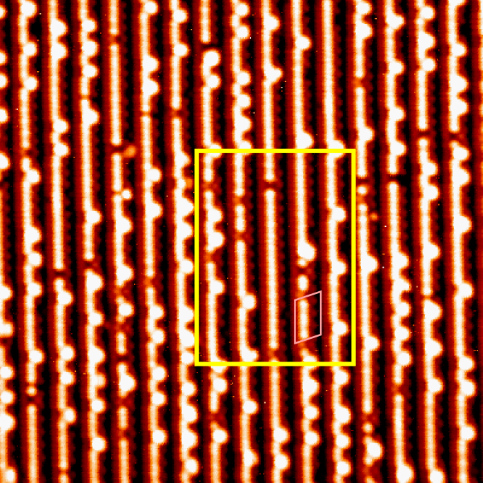
Figure 2 shows enlarged part of the image marked with thick line in Fig. 1 recorded at tunneling current nA and the sample bias V (a) and V (b).
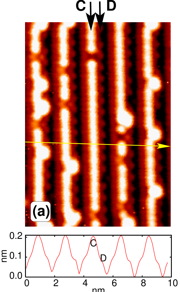
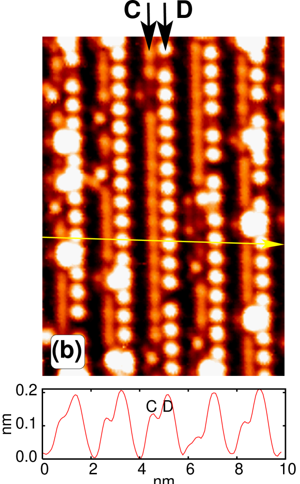
We note that images (a) and (b) represent the same area of the sample. The STM images clearly show sets of double chains on each terrace. Distance between these sets is equal to the width of the unreconstructed Si(557) surface terrace, ( nm), and the distance between two chains on the same terrace is equal to ( nm). However the chains on the same terrace show different behavior. While the chain indicated by arrows and denoted as C in Fig.2 (a) and (b) is apparently continuous and very similar to that grown on Si(335)-Au surface MK_1 , the wire D differs considerably and reminds a row of well ordered single atoms rather than one-dimensional object. However periodicity along chains are the same in both wires and equal to ( nm). It is worth to note that similar periodicity along the chain has been also found in different structures, like Si(335)-Au MK_1 with single chain per terrace or Si(111)-(5 2)-Au Erwin with double Au chains.
As one can read from the figure both chains show oscillations of the electron density with distance along their length. Moreover, it is clearly seen that those chains behave differently upon reversing the sample bias. Topography of the nanowire C (top picture) reverses (maxima change into minima and vice versa) with switching of the voltage bias from negative to positive values. Such behavior has been previously observed in the case of Si(335)-Au structure MK_1 and has strictly electronic origin. On the other hand there is a lack of such reversing in the chain D where its topography remains almost unchanged, except that at positive bias the structures are higher. We stress that in order to exclude possible influence of the sample thermal drift the presented STM images were recorded simultaneously, with negatively biased sample during line forward scan and positively biased during line backward scan.
It is interesting to see the changes of topography with the bias voltage. The evolution of topography changes with the bias voltage is shown in Fig. 4.
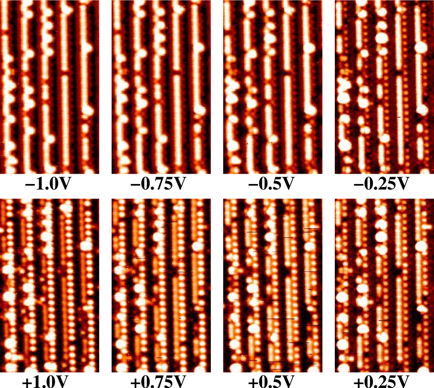
We observe that the chains of C (D) type simultaneously become less (more) visible while going from negative to positive biases. Moreover, chains of D type do not show any topography reverse. On the other hand, there is a reverse of the topography of the C type chains when crossing zero bias.
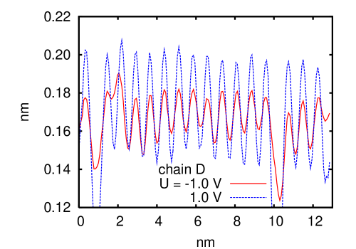
Another interesting effect is associated with recently observed zero dimensional end states Crain_2 . Such states must have the wave function localized to the end atoms in a chain, and it must must decay exponentially into the chain Davison ; Crain_2 . Similarly for Si(553)-Au surface Crain_2 , we observe that C type chains at negative sample bias appear longer than at positive bias (see Fig. 3 - top panel). At negative bias the end atoms are well visible while for negative bias the atoms second form the end are enhanced and the end atoms became supressed. This fact can be explained in terms of different densities of states above and below the Fermi energy (see discussion in Sec. IV). However, unlike in Ref. Crain_2 , the topography modulation along chain is twice a lattice constant ( nm) and what is important we also observe the topography reverse. We stress that there is no such an effect for chains of D type (see Fig. 3 - bottom panel).
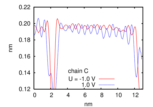
To see the evolution of the topography of chain C type with the sample bias we show in Fig. 5 the cross sections along the longest chain indicated by arrow with label C in Fig. 2.
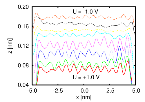
It is clearly visible how the length of the chain becomes shorter going from negative to positive voltages. Moreover around zero bias we observe the reverse of the topography.
Figure 6 shows the length of above discussed the chain as a function of the sample bias.
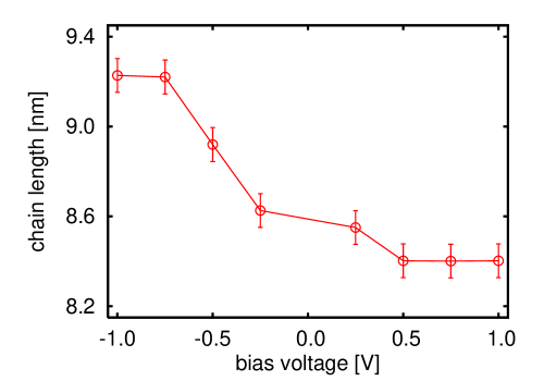
We define the length as a distance between endmost maxima in the topography profile (see Fig. 5). We observe that the effect associated with the length changing of the chain takes place in the range between V to V. Below the bias V and above V it remains almost constant, and the length difference between those biases is equal nm (twice a lattice constant along the chain).
From the experimental data we cannot judge what material (Si or Au) those wires are composed of. Certainly there is no sufficient amount of gold to produce two gold chains within terrace, unless we assume that gold atoms occupy every second site in direction , which would be supported by fact that those chains show oscillations with period twice as large as the lattice constant in this direction. However it is difficult to find any particular reason supporting this assumption. So one can assume that we deal with one gold and one silicon chains. This would be supported by above-mentioned differences between chains seen in STM images. However there might be another scenario in which both structures come from silicon whilst gold atoms substitute into the surface producing a third chain not visible in STM images. Such supposition is supported by the fact that Au is more electronegative than Si and binds one Si electron with their , electrons in a low laying state Sanchez , according to the first principle calculations Crain_1 ; Sanchez_1 . The chain structures visible in STM are likely to be Si atoms at step edge (chain C), similar to those in Si(335)-Au, and Si adatoms (chain D).
III Theoretical description
The experimental studies suggest that the electronic states in the chain C have extended nature while in chain D they are localized. In the language of the tight binding model the hopping integral between atoms in chain C has larger value than that in the other chain or single particle electron energies of the chain C atoms lay much closer to the Fermi energy of the surface than those of the chain D. So one can conclude that chain C has metallic character whilst D is of isolating (semiconducting) nature. Moreover, the fact that at negative sample bias (Fig. 2 a)) chain C is more visible in the STM topography image than the chain D while at positive (Fig. 2 b)) the effect is opposite, suggests that we deal with mainly occupied states in the chain C and empty states in D.
In order to explain the effect associated with the electron density oscillations and differences between neighboring chains observed in STM images, we propose a model of two coupled non-equivalent chains composed of Au (chain C) and Si (chain D), schematically depicted in Fig. 7.
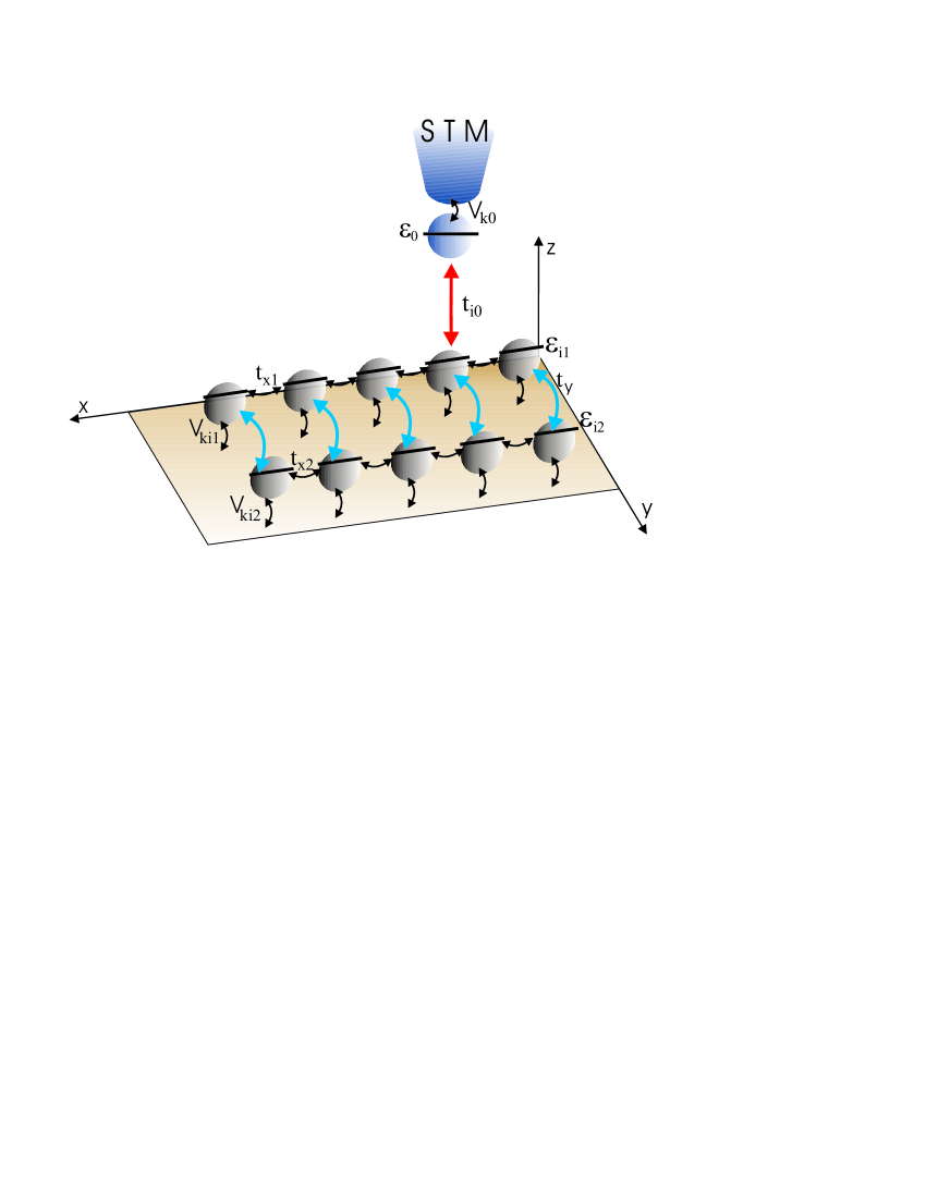
The Hamiltonian describing system composed of surface, two chains and STM tip is:
| (1) |
where
| (2) |
is for STM electrode electrons with single particle energies . The STM tip is modeled by single atom with energy level
| (3) |
The wire part of the Hamiltonian is described by
| (4) |
where is the atomic energy of the -th atom in chain , is the hopping integral between neighboring atoms in the same chain, while - hopping between neighboring atoms in different chains. Hamiltonian of the surface is
| (5) |
and interactions between different subsystems are in the form
| (6) |
with being hybridization between STM electrode electrons and STM tip, - hopping between atoms in a chain and STM tip and finally - hybridization matrix element connecting surface and the chain . In all above equations we have omitted spin index in the electron creation (annihilation) operators as we are not interested in magnetic properties and assume that system is in paramagnetic phase.
In order to calculate the tunneling current from the STM electrode to the surface we follow the standard derivations Haug ; Niu ; MK_2 and get
| (7) |
where is the Fermi distribution function of the STM (surf) electrode with the chemical potential and the transmittance is given in the form
| (8) |
and is the coupling parameter between STM electrode and the tip atom and surface and the chain respectively. is the the Fourier transform of the retarded GF , and is the matrix element (connecting the tip atom with -th atom in chain ) of full GF, solution of the equation
| (9) |
Full GF is matrix ( atoms in a wire , atoms in a wire and the tip site), which has to be determined, just by inverting matrix . Note that within the present model there are no Coulomb interactions between electrons and the problem can be solved exactly.
IV Numerical results
So far we are able to calculate the tunneling current for a given bias voltage at constant STM tip - surface distance. In our model, the quantity which is related to this distance is the coupling between tip atom and the chain (in units of ). From the physics of tunneling phenomena we know that exponentially depends on distance between STM tip and the chain. A rough estimate of may be deduced by taking both the tip and the chain orbitals as the lowest states of square potential wells of spatial widths separated by the barrier of height equal to the work function and width equal to the distance between STM tip and the chain. The half of the ground state energy splitting in this double well structure is thus given by Calev :
| (10) |
where is the electron mass, - work function taken as , - length parameter (of order of an orbital spatial size) chosen as in units of the lattice constant .
In numerical calculations we have chosen the Fermi energy of the surface as zero of energy scale (). All energies are measured with respect to it in units of and for simplicity we have chosen . The quantities concerning distances are expressed in units of the lattice constant along chain (). Moreover, the distance between chains is modeled via inter-chain hooping integral .
To get the information on topography of the wire we have solved Eqs.(7)-(9) self-consistently for a given bias voltage and fixed current , got value of and finally determined from relation (10).
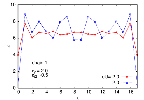
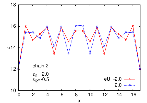
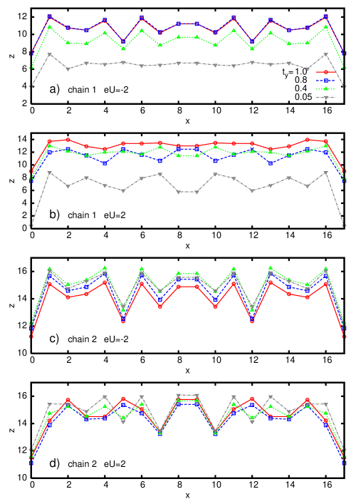
In Fig. 8 we show the comparison of the STM tip - surface distance along chains and for negative and positive sample biases.
It is clearly seen that chain (corresponding to the chain C observed in experiment) shows the bias dependent reverse of the topography (top panel) while chain (chain D) is insensitive to it (bottom panel). Furthermore, if the atomic energies of the chain are close to the Fermi energy, the topography of the chain remains almost unchanged with respect to the reverse of the bias voltage, while it reverses if the chain atomic energies lay far away from the Fermi energy. We have performed a number of calculations for various values of and this seems to be a general tendency, provided the other parameters are the same for both chains. Actually this can be understood from a simple argument if we consider not a chain but single atom with atomic energy . Namely, the atomic local density of states (LDOS) has Lorentzian shape due to the coupling to the STM tip and the surface, and if is close to the Fermi energy, the LDOS is almost symmetric with respect to the Fermi energy. Tunneling current is an integral of the LDOS bounded by the chemical potentials of the STM tip and surface electrodes, so it gives approximately the same values of the current for both voltage polarizations and therefore no topography reverse. In opposite situation, if the atomic energy is far away from the the Fermi energy, the LDOS is strongly asymmetric and centered around , thus giving a different contributions to the current. If lays within (between and ) tunneling occurs through the main peak of the LDOS giving large value of the current while in opposite situation the contribution is small as the tunneling takes place only through the tail of the main peak in the LDOS.
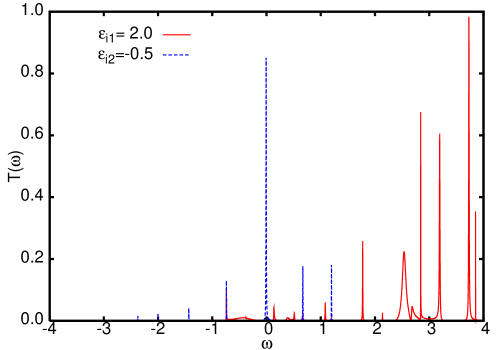
Similar argument applies to the chain, however density of states (DOS) is now more complicated as it contains many peaks. Again, if the chain single particle energies lay close to the Fermi energy, the DOS is almost symmetric and thus no topography reverse. If are much larger than the Fermi energy, density of states contains a series of peaks distributed mainly around original values of , and therefore we get a large current for given bias sample and small one for reversed bias. This is clearly seen in Fig. 9, where the example of the weighted DOS (transmittance) at STM tip position in the middle of the chain (see Fig. 8) is plotted as a function of energy.
Turning to the experimental data, one can associate chain C with the chain in Fig. 8 (top panel) and chain D with that indicated by in Fig. 8 (bottom panel) and conclude that chain C (Fig. 2) consists of single atoms with atomic energies much larger than the Fermi energy, while chain D has those energies close to the Fermi energy assuming that the other parameters characterizing chains are equal for both chains.
At this point it is interesting to note boundary effects clearly seen in Fig. 8 (bottom panel) and associated with the zero dimensional states at the ends of the chains, recently observed on Si(553)-Au surface Crain_2 .
Another important quantity is the inter-chain hopping integral . In Fig. 10 the STM tip - surface distance is plotted for different values of the inter-chain couplings .
It is clearly seen that the strength of the coupling can modify results. However, while it has strong influence on the properties of the chain , eventually leading to the reverse of the topography for positive bias (compare curve with boxes () with the others in the panel b)), it very weakly modifies topographic properties of the chain . Such a difference in the influence can be explained in the following way. As we would expect the inter-chain hopping modifies the transmittance of the system. It shifts the positions of the resonances in the in both chains in the same way but at the same time it modifies their spectral weights in different way. However for close to the Fermi energy the transmittance integrated over the remains almost unchanged, thus leading to similar values of the tip - surface distance for different inter-chain couplings .
Let us now discuss what the effect of the hopping integral between between neighboring atoms in the same chain on the topography is. Figure 11 shows the topography of the chains for a number of the intra chain hopping integrals with fixed and , .
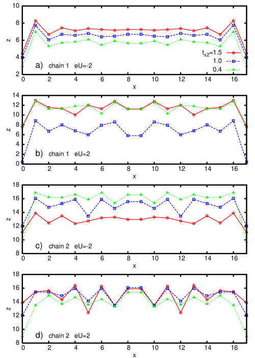
It is clearly seen that the intra chain hopping can change the topography of the chain. While for larger values of the hopping along chain than that along chain () one can observe reverse of the topography in both chains (compare curves with circles in all panels), for equal hoppings () there is a reverse of the topography in chain and no such effect in chain (curves with boxes) and for () there is no reverse of the topography in either chain (curves with triangles). Such modifications of the chain topography due to the intra chain hopping integrals is not a general property of the system as there is no similar effect in the symmetric situation, namely if the chain atomic energies were equal. We have performed a number of calculations for and got quite different behavior from that presented in Fig. 11. Namely, our self-consistent calculations always converged to the results showing the reverse of the topography in both chains. This is a very important result as it leads to the conclusion that the chain atomic energies have to be different in both chains in order to get an agreement with the experimental data.
Similar effect on the topography has the coupling to the surface . For one always gets reverse of the topography in both chains. This can be easily understood if we remind that coupling to the surface leads to the broadening of the resonances in the density of states but does not influence their positions when the Coulomb interactions in chains are neglected.
From above discussion one can conclude that the main effect which leads to the reverse of the topography in one chain and its lack in the other one comes from the chain atomic energies - they have to be different in both chains. Going further one can conclude that the chains observed in STM have been made of different materials, one of silicon and the other one of gold.
V Comparison with experiment
To make quantitative comparison of the theoretical calculations with the experimental data we use the formula for the tip - surface distance (10) and put eV and nm.
Figure 12 shows both the experimental and the theoretical data of typical short chains of type C and D, marked with smaller box in Fig. 1.
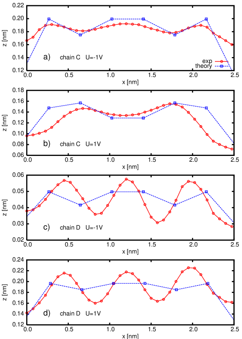
The best fit has been obtained with the chain atomic energies eV for chain C and eV for chain D, respectively. Moreover, the values of the intra-chain and inter-chain hoppings were the same as those obtained in Ref. Crain_1 , i.e. eV and eV. Those values of the chain atomic energies, as it was stated previously, suggest that we deal with different chains, i.e. chains composed of different materials. Going further, we can assign the C chain to the Si atoms, while D chain to the Au atoms. This can be deduced from different values of the atomic energies used in calculations and electronegativity of free atoms. The Au atoms are more electronegative, so they should have lower atomic energies, eV in our case, while Si atoms have eV. Of course, this conclusion is true provided the other parameters are the same or similar in both chains.
Although theoretical topography curves do not exactly follow experimental ones, main features, i.e. the reverse of the topography for chain C and its lack for chain D, are quite reasonably reproduced. The deviations between theoretical calculations and experimental data steam from the fact that we used a simple model of STM tunneling, nevertheless giving a semi-quantitative agreement with the experiment. Moreover, our model allows for calculations of the tunneling current in the cases when the STM tip is placed exactly above the chain atom, therefore we do not present the theoretical data for the tip position between chain atoms. To get full agreement with experimental data one has to take into account additional effects, like tunneling into aside chain atoms, the Coulomb interactions or perform first principles calculations which is out of the scope of the present work.
VI Conclusions
In conclusion we have studied properties of the mono-atomic chains on the vicinal Si(557)-Au surface using STM technique. We have observed double non-equivalent chains on such surface showing different behavior of the topography with reversing of the bias voltage. While chain C shows reverse of the topography, chain D does not show such effect. Additionally the STM tip - surface distance oscillates along any chain with the same period equal to double lattice constant in direction . We have also performed tight binding model calculations showing similar oscillations of the STM tip - surface distance and led us to the conclusion that atomic energies have to be different in different chains and larger in chain C than in chain D. This fact supports the scenario which is probably realized in experiment that one chain is made of gold (chain D) and the other one of silicon atoms (chain C).
Acknowledgements.
This work has been supported by the KBN grant no. 1 P03B 004 28. T. K. thanks the Foundation for Polish Science for a Fellowship for Young Scientists.References
- (1) F. J. Himpsel, K. N. Altmann, R. Bennewitz, J. N. Crain, A. Kirakosian, J. -L. Lin, J. L. McChesney, J. Phys.: Condens. Matter 13, 11097 (2001).
- (2) J. M. Luttinger, J. Math. Phys. 4, 1154 (1963).
- (3) F. D. M. Haldane, J. Phys. C: Solid State Phys. 14, 2585 (1981).
- (4) R. E. Peierls, in Quantum Theory of Solids, Clarendon, Oxford (1955).
- (5) M. Jałochowski, E. Bauer, Prog. Surf. Sci. 67, 79 (2001); Surf. Sci. 480, 109 (2001).
- (6) R. Zdyb, M. Stróżak, M. Jałochowski, Vacuum 63, 107 (2001).
- (7) J. N. Crain, A. Kirakosian, K. N. Altmann, C. Bromberger, S. C. Erwin, J. L. McChesney, J. -L. Lin, F. J. Himpsel, Phys. Rev. Lett. 90, 176805 (2003).
- (8) J. N. Crain, J. L. McChesney, Fan Zheng, M. C. Gallagher, P. C. Snijders, M. Bissen, C. Gundelach, S. C. Erwin, F. J. Himpsel, Phys. Rev. B69, 125401 (2004).
- (9) M. Krawiec, T. Kwapiński, M. Jałochowski, phys. stat. sol. (b) 242, 332 (2005).
- (10) M. Henzler, R. Zhachuk, Thin Solid Films 428, 129 (2003).
- (11) M. Jałochowski, M. Stróżak, R. Zdyb, Surf. Sci. 375, 203 (1997).
- (12) P. Segovia, D. Purdie, M. Hengsberger, Y. Baer, Nature (London) 402, 504 (1999).
- (13) R. Losio, K. N. Altmann, A. Kirakosian, J. -L. Lin, D. Y. Petrovykh, F. J. Himpsel, Phys. Rev. Lett. 86, 4632 (2001).
- (14) K. N. Altmann, J. N. Crain, A. Kirakosian, J. -L. Lin, D. Y. Petrovykh, F. J. Himpsel, Phys. Rev. B64, 035406 (2001).
- (15) D. Sanchez-Portal, J. D. Gale, A. Garcia, R. M. Martin, Phys. Rev. B65, 081401 (2002).
- (16) I. K. Robinson, P. A. Bennett, F. J. Himpsel, Phys. Rev. Lett. 88, 096104 (2002).
- (17) D. Sanchez-Portal, R. M. Martin, Surf. Sci. 532, 655 (2003).
- (18) H. Okino, R. Hobara, I. Matsuda, T. Kanagawa, S. Hasegawa, J. Okabayashi, S. Toyoda, M. Oshima, K. Ono, Phys. Rev. B70, 113404 (2004).
- (19) R. A. Zhachuk, S. A. Teys, A. E. Dolbak, B. Z. Olshanetsky, Surf. Sci. 565, 37 (2004).
- (20) A. A. Baski, K. M. Jones, K. M. Saoud, Ultramicroscopy 86, 23 (2001); A. A. Baski, K. M. Saoud, K. M. Jones, Appl. Surf. Sci. 182, 216 (2001); J. W. Dickinson, J. C. Moore, A. A. Baski, Surf. Sci. 561, 193 (2004).
- (21) S. S. Lee, N. D. Kim, C. G. Hwang, H. J. Song, J. W. Chung, Phys. Rev. B66, 115317 (2002).
- (22) J. R. Ahn, Y. J. Kim, H. S. Lee, C. C. Hwang, B. S. Kim, H. W. Yeom, Phys. Rev. B66, 153403 (2002).
- (23) S. Jeong, H. Jeong, S. Cho, J. M. Seo, Surf. Sci. 557, 183 (2004).
- (24) S. C. Erwin, Phys. Rev. Lett. 91, 206101 (2003).
- (25) J. N. Crain, D. T. Pierce, Science 307, 703 (2005).
- (26) S. G. Davison, M. Steślicka, Basic Theory of Surface States, Oxford Univ. Press, New York (1992).
- (27) Y. Calev, H. Cohen, G. Cuniberti, A. Nitzan, D. Porath, Israel J. Chem. 44, 133 (2004).
- (28) H. Haug, A. P. Yauho, Quantum Kinetics in Transport and Optics of Semiconductors, Springer, Berlin (1996).
- (29) L. V. Keldysh, Sov. Phys. JETP 20, 10 108 (1965).
- (30) C. Niu, D. L. Lin, T. -H. Lin, J. Phys.: Condens. Matter 11, 1511 (1999).
- (31) M. Krawiec, K. I. Wysokiński, Solid State Commun. 115, 141 (2000); Supercond. Sci. Technol. 17, 103 (2004).