Two-Dimensional Electron Gas in InGaAs/InAlAs Quantum Wells
Abstract
We designed and performed low temperature DC transport characterization studies on two-dimensional electron gases confined in lattice-matched In0.53Ga0.47As/In0.52Al0.48As quantum wells grown by molecular beam epitaxy on InP substrates. The nearly constant mobility for samples with the setback distance larger than 50nm and the similarity between the quantum and transport life-time suggest that the main scattering mechanism is due to short range scattering, such as alloy scattering, with a scattering rate of 2.2 ps-1. We also obtain the Fermi level at the In0.53Ga0.47As/In0.52Al0.48As surface to be 0.36eV above the conduction band, when fitting our experimental densities with a Poisson-Schrödinger model.
pacs:
PACS number(s): 68.65.+g; 73.50-h;Two dimensional electron gas (2DEG) confined in In0.53Ga0.47As in lattice matched InGaAs/InAlAs/InP heterostructures and superlattices appear in many technologically important areas ranging from high speed electronicsmishra , optoelectronicswang ; tred and spintronicsnitta ; koga . It is also an attractive 2DEG system for the study of disorder induced quantum phase transitions Wei ; Sahar ; Wei2 ; pan ; Hilke ; Einat . While there have been several earlier works characterizing electronic properties of 2DEGs in In0.53Ga0.47As/In0.52Al0.48As heterojunctionskast ; walu ; nakata ; matsu , In0.53Ga0.47As/InP heterojunctions and quantum wells (QW)weiapl ; frei ; grutz , there were few systematic studies characterizing 2DEGs in In0.53Ga0.47As/In0.52Al0.48As QWs. Since many modern structures mishra ; wang ; tred ; koga are now based on In0.53Ga0.47As/In0.52Al0.48As QWs, such characterization is of fundamental and technological interest.
In this letter we report the characterization of electronic properties of 2DEG in a series of lattice matched InGaAs/InAlAs QWs grown by molecular beam epitaxy (MBE) on InP substrate (here and after in our paper we use abbreviations InGaAs for In0.53Ga0.47As and InAlAs for In0.52Al0.48As). Systematic investigations of 12 such wafers with varying design parameters in the doping layers have yielded important information not only about carrier mobility and scattering, but also about how doping determines the carrier densities, from which we were also able to determine the location of the Fermi level at the InGaAs surface.
The schematics of the samples is depicted in Fig. 1(a) and the parameters for each sample are summarized in Table 1. The 2DEG resides in a 20nm-wide InGaAs QW. Two Si -doped layers are placed in the InAlAs barrier to one side (closer to the surface) of the QW. The three design parameters that were varied are the doping densities ( and ) in the top and bottom dopant layers respectively, and the distance from the bottom dopant layer to the (top) edge of the QW.
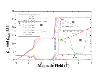
We fabricated standard Hall bars with Indium ohmic contacts. We tried to measure all the samples at dark. Except a few samples () most of them need to be illuminated to create a 2DEG. For these samples we illuminated for sufficient time with an LED to create a 2DEG with the highest possible mobility. We measured the magnetoresistance and the Hall resistance as a function of the perpendicular magnetic field (B) for different temperatures. The results are shown in Fig. 1 for the sample (see Table 1). Similar results were obtained for the other samples. From the measured data we obtain the areal density and the mobility of the electrons, from which we can extract the transport lifetime . We used an effective mass for In0.53Ga0.47As of 0.043 times the bare electron massvurgaftman . From the onset of SdH oscillations we extracted also the quantum lifetime () by using a Dingle style analysis. The amplitude () of the envelope function of the SdH oscillations was found to be well described by the conventional Ando formula coleridge ; johndavies , where , is the cyclotron frequency and represents the resistance at zero applied magnetic field, for a given value of temperature. To obtain the amplitudes (), for each temperature we fitted the envelope of the SdH oscillations to a pair of polynomials as showed in Fig. 1(b) for T=1300 mK. Next we obtained just subtracting both polynomials and we plotted versus in a log-x graph as in Fig. 1(c). From the previous mentioned Ando formula, we performed a linear fit to achieve the slope () of the Dingle plot [Fig. 1(c)] and obtain the quantum lifetime for the given temperature as . Table 1 summarizes our results measured at 4.2 K, together with relevant parameters of the samples.
| Sample | |||||||
|---|---|---|---|---|---|---|---|
| number | (nm) | (/cm2) | (/cm2) | (/cm2) | () | (ps) | (ps) |
| 1 | 0.11 | 0.17 | |||||
| 2 | 0.31 | 0.22 | |||||
| 3 | 0.39 | 0.31 | |||||
| 4 | 0.35 | 0.31 | |||||
| 5 | 0.39 | 0.32 | |||||
| 6 | 0.38 | 0.31 | |||||
| 7 | 0.37 | 0.31 | |||||
| 8 | 0.37 | 0.31 | |||||
| 9 | 0.37 | 0.31 | |||||
| 10 | 0.38 | 0.33 | |||||
| 11 | 0.36 | 0.31 | |||||
| 12 | 0.38 | 0.31 |
Our measurements show no indication of parallel conduction nor any presence of a second subband. We have also confirmed this by solving self-consistently the Schrödinger and Poisson equations to calculate the subband energy levels. The calculation shows that only one subband is occupied and the second subband is more than 40 meV above the Fermi level. To understand the origin of the electrons forming the 2DEG, we solved analytically the electrostatic Poisson equation for our structure following similar procedures as in Ref. johndavies, and assuming full ionization of dopants. This leads to the following analytical expression for for our structure,
| (1) |
where , , are as defined earlier, =50nm is the thickness of the InGaAs cap layer, =18nm is the distance from the top Si -doped layer to the upper-end of the InAlAs and =150nm the distance between the two Si -doped layers; =14.2 is the relative dielectric constant of InGaAsWatling and is the offset of the fermi level at the InGaAs surface with respect to the conduction band edge. In the denominator, is an effective “quantum” depth of the 2DEGjohndavies which turns out to be approximately the QW width (20nm) in our case (the deviation is negligible compared to the contribution from other terms in the denominator). If we plug-in all the relevant numerical values, we get the following dimensionless formula for :
| (2) |
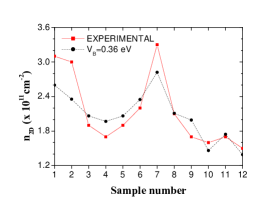
where , , and are in units of cm-2, in nm, and in eV. The only free parameter in our model, , is the Fermi level relative to the conduction band edge (CBE) at the InGaAs surface. Due to surface states, the local Fermi level at a semiconductor surface is often pinned regardless of doping and carrier density. For example, the surface Fermi level for GaAs is about eV below the CBE. For InGaAs, such information is largely unknown, hence we have fitted this parameter using our data and the best fit is obtained for eV. Here, the surface Fermi level is above the CBE, which is very similar to the InAs case tsui70 , except that in our samples, it appears that the surface carriers are not mobile enough and do not contribute significantly to the transport.
In Fig. 2, is plotted as a function of sample number, with eV. Clearly, there is an excellent agreement, between this fit (2) and the experimental data. This also confirms that is only a function of , and and indicates that unintentional doping from the residual or background impurities does not appear to be significant in our samples. Indeed, introducing background impurities in our model would lead to a decrease of the features seen in Fig. 2 and therefore does not fit our data as well. From the data in Table 1, we can notice that for larger than 50nm, the mobilities and the lifetimes are independent of the doping parameters (, and ). In Fig. 3 we plot the quantum scattering rate (triangles) and the transport scattering rate (circles), measured at 4.2K for samples 1-3 and 10-12, as a function of , the distance from the bottom doping layer to the quantum well. Both scattering rates () shows a fast decrease at small values of (below 30nm), indicating that the dopants provide efficient scattering for electrons at short . For of 50 nm or more, however, becomes independent of . From samples with =50nm but different and , we found to be also independent of the doping densities, as is shown, for example, in the inset (a) of Fig. 3 where is plotted against at =50 nm. Our findings indicate that, for 50nm, the dopant layers are not the major source of carrier scattering in these structures. The common and reproducible value of mobility (15000 cm2/Vs) observed for wafers (with 50 nm) from different MBE growth suggests that the mobility, or carrier scattering originates from some intrinsic, non-doping related scattering in our structures. Moreover, since the dependence of the mobility on the 2DEG density is very weak as seen in Table 1, we believe that an important source of scattering is due to the random alloy scattering potential, which is expected to have a weak density dependenceBastard . Such intrinsic alloy scattering is clearly very important in the In0.53Ga0.47As channel, as claimed previously to dominate the low temperature scattering in InGaAs/InAlAs heterojunctionswalu ; matsu . We further believe that surface roughness is less important since these structures are lattice matched MBE grown and because surface roughness would lead to a stronger dependence of mobility on density. Hence the main source of disorder is short-ranged in contrast to charged doping disorder, which is long ranged, in relation to the Fermi wavelength. The short range nature of the dominant scattering mechanism for our samples with 50nm is consistent with our observation that the quantum life time is similar to the transport lifetime. We have measured the scattering rate dependence at lower temperatures (), as shown in inset (b) of Fig. 3 for representative data in sample 5, from which we extract a low limiting value of the scattering rate to be 2.2 ps-1.
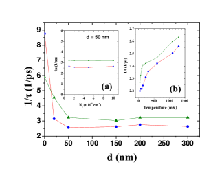
Since most samples have to be illuminated in order to obtain the optimum mobility, it is likely that DX centers play a role maude ; chadi ; baraldi . We therefore estimated their contribution by fitting, for the sample 5, the temperature dependence of the total density to where cm-2 and . The best fit is obtained for cm-2 and meV (below the Fermi energy). Hence, DX centers could explain the observed increasing of both the 2DEG density and of the scattering rate with increasing temperature. Indeed, at higher temperatures, more carriers are activated, which will also leave the DX centers unsaturated and lead to the increased scattering rate as seen in Fig. 3(b).
In conclusion, we have studied the two-dimensional electron system confined in MBE-grown In0.53Ga0.47As/In0.52Al0.48As quantum wells. We have measured 12 different wafers specifically designed and grown to investigate transport properties of this type of material. We have obtained an analytical expression for the of our samples with a very good agreement with the measured values, showing that depends only on parameters of the Si -doped layers (, and ). We obtain an excellent fit to our experimental densities assuming the In0.53Ga0.47As surface Fermi energy to be above the conduction band. For setback distance of 50nm or more, quantum and transport scattering rates are independent of parameters of the dopant layers and are likely mainly due to short-range scattering, such as alloy scattering, for which a scattering rate of 2.2 ps-1 is extracted at 22 mK.
We thank to Dan Tsui and Leonard Brillson for helpful discussions. E. Diez acknowledges supports from MEC (Ramón y Cajal and FIS2005-01375), JCyL (SA007B05), EC (DIEZ-WISSMC/RITA-CT-2003-506095) and the hospitality of the Braun Submicron Center. Y.Chen acknowledges supports from NSF and a Gordon Wu Fellowship.
References
- (1) U. K. Mishra, U. S. Brown, M. J. Delaney, P. T. Greiling, C. F. Krumm, IEEE Trans. Microwave Theory Tech. 37, 1279 (1989)
- (2) Y. H. Wang, S. S. Li, P. Ho, Appl. Phys. Lett. 62, 621 (1993).
- (3) A. Tredicucci, C. Gmachl, F. Capasso, D. L. Sivco, A. L. Hutchingson, A. Y. Cho, Nature, 396, 350 (1998).
- (4) J. Nitta, T. Akazaki, H. Takayanagi, T. Enoki, Phys. Rev. Lett. 78, 1335 (1997).
- (5) T. Koga, J. Nitta, T. Akazaki, H. Takayanagi, Phys. Rev. Lett. 89, 046801 (2002).
- (6) H. P. Wei, D. C. Tsui, M. A. Paalanen, A. M. M. Pruisken, Phys. Rev. Lett. 61, 1294 (1988).
- (7) D. Sahar, M. Hilke, C. C. Li, D. C. Tsui, S. L. Sondhi, J. E. Cunningham, M. Razeghi, Solid State Commun. 107, 19 (1998).
- (8) R. T. F. van Schaijk, A. de Visser, S. M. Olsthoorn, H. P. Wei, A. M. M. Pruisken, Phys. Rev. Lett. 84, 1567 (2000).
- (9) W. Pan, D. Shahar, D. C. Tsui, H. P. Wei, and M. Razeghi, Phys. Rev. B. 55, 15431 (1997).
- (10) M. Hilke, D. Shahar, S. H. Song, D. C. Tsui, M. Shayegan and Y. H. Xie, Ann. Phys. (Leipzig) 8, 603 (1999).
- (11) E. Peled, D. Shahar, Y. Chen, E. Diez, D.L. Sivco and A.Y. Cho, Phys. Rev. Lett. 91, 236802 (2003).
- (12) A. Kastalsky, R. Dingle, K. Y. Cheng, and A. Y. Cho, Appl. Phys. Lett. 41, 274 (1982).
- (13) W. Walukiewicz, H. E. Ruda, J. Lagowski, and H. C. Gatos, Phys. Rev. B. 30, 4571 (1984).
- (14) Y. Nakata, S. Sasa, Y. Sugiyama, T. Fujii and S. Hiyamizu, Jpn. J. Appl. Phys. 26, L59 (1987).
- (15) T. Matsuoka, E. Kobayashi, K. Taniguchi, C. Hamaguchi, S. Sasa., Jpn. J. Appl. Phys., 29, 2017 (1990).
- (16) H. P. Wei, D. C. Tsui, M. Razeghi, Appl. Phys. Lett. 45, 666 (1984).
- (17) M. Frei, D. C. Tsui, and W. T. Tsang, Appl. Phys. Lett. 50, 606 (1987).
- (18) D. Grützmacher, R. Meyer, P. Balk, C. Berg, T. Schäpers, H. Lüth, M. Zachau and F. Koch, J. Appl. Phys., 66, 697 (1989).
- (19) I. Vurgaftman, J. R. Meyer, and L. R. Ram-Mohan, J. Appl. Phys., 89, 5815 (2001)
- (20) P. T. Coleridge, R. Stoner, R. Fletcher, Phys. Rev. B 39 1120 (1989).
- (21) J. H. Davies, The Physics of Low Dimensional Semiconductors, Cambridge University Press (1999).
- (22) J. R. Watling, A. B. Walker, J. J. Harris, J. M. Roberts, Semicond. Sci. Tech. 14, 12 (1999).
- (23) D. C. Tsui, Phys. Rev. Lett. 24, 303 ( 1970)
- (24) G. Bastard, Wave Mechanics Applied to Semiconductor Heterostructures (Halsted, New York, 1988).
- (25) D. K. Maude, J. C. Portal, L. Dmowski, T. Foster, L. Eaves, M. Nathan, M. Heiblum, J. J. Harris, R. B. Beall, Phys. Rev. Lett. 59, 815 (1987).
- (26) D. J. Chadi and K. J. Chang, Phys. Rev. B 39, 10063 (1989).
- (27) A. Baraldi, P. Frigeri, C. Ghezzi, A. Parisini, A. Bosacchi, S. Franchi, E. Gombia, R. Mosca, Phys. Rev. B 53, 10715 (1996).