Ground-state characterization of Nb charge-phase Josephson qubits
Abstract
We present investigations of Josephson charge-phase qubits of SQUID-configuration inductively coupled to a radio-frequency-driven tank circuit enabling the readout of the states by measuring the Josephson inductance of the qubit. The circuits including junctions with linear dimensions of nm nm and nm nm are fabricated from Nb/AlOx/Nb trilayer and allow the determination of relevant sample parameters at liquid helium temperature. The observed partial suppression of the circulating supercurrent in the qubit loop at 4.2 K is explained within the framework of a quantum-statistical model. We have probed the ground-state properties of qubit structures with different ratios of the Josephson coupling to Coulomb charging energy at 20 mK, demonstrating both the magnetic control of phase and the electrostatic control of charge of the qubit.
pacs:
74.50.+r, 85.25.Cp, 73.40.GkI Introduction
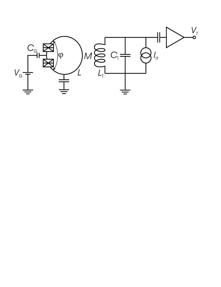
Superconducting structures with mesoscopic Josephson tunnel junctions can provide a basis for electronic devices operating on single Cooper pairs. Prominent examples are the superconducting quantum bit (qubit) circuits which are regarded as promising elements for a scalable quantum computer makhklin01 . The Josephson charge-phase qubit cpqb1 is based on a Cooper-pair box qpbox of SQUID-configuration, i.e. a superconducting loop interrupted by two small-capacitance junctions with an island in between, which is capacitively coupled to a gate electrode (i. e. the Bloch transistor q-SG ). The charging energy and the Josephson coupling energy are typically of the same order, so the dimensionless parameter is of the order of one. Moreover, our circuit comprises both the qubit and its readout cpqb2 . The transistor can be operated as a box (qubit) whose distinct quantum states with energies are associated with different Bloch-bands of the system sqc . The eigenfunctions are the Bloch wave functions of a particle in the periodic (Josephson) potential. Here is the band number and the quasicharge governed by the gate voltage , i. e. , where is the gate capacitance, see, e.g., Ref. zorin96 . The quantum states of the transistor also involve the phase coordinate set by the external magnetic flux applied to the SQUID loop. The variable behaves almost classically and is regarded as a parameter. Due to two control parameters (charge and phase), the eigenenergies , the transition frequency as well as - in the case of multiple qubits - the strength of mutual coupling, can be varied in the wide range. The read-out of our qubit can be performed similar as in the rf-SQUID-based impedance measurement technique pioneered by Rifkin and Deaver rifkin76 : the qubit eigenstates can be distinguished by the Josephson inductance of the effective weak link, i.e. the transistor, included in the loop whose impedance is probed by small rf-oscillations induced by an inductively coupled resonant tank circuit cpqb2 ; zorin03 , see the equivalent circuit in Fig. 1.
Recently, Born et al. imt2 have confirmed the aforementioned read-out conception in the spectroscopic experiment with Al qubit. The authors demonstrated the detection of microwave-power-induced interband transitions by tracking the resonant response of the tank. However, due to the rather large ratio , manipulation of the qubit state via its gate was in their experiment limited to a narrow (about 5%) interval of values of the flux. In this paper, we present a comprehensive mapping of the ground state of Nb qubits operating in the charge-phase regime over a wide range of the parameters and . This is done for the most illustrative case of the values of the parameter . In this regime, the behaviour of the system strongly depends on the value of . Moreover, the effect of thermal fluctuations is studied comparatively at 20 mK and 4.2 K for the same samples. These investigations strongly benefit from the advanced technology for the fabrication of sub–m Josephson junctions based on Nb/AlOx/Nb trilayers with a large superconducting energy gap and a low sub-gap leakage current dolata05 . Applying this technology allows all inductive components of the circuitry shown in Fig. 1 to be integrated on one chip.
The material presented in this paper is organized as follows. In Sec. II, we briefly outline the considerations that motivated our choice of experimental parameters. In Sec. III, radio-frequency measurement results for niobium-based Bloch transistors will be presented and quantitatively analyzed. Especially the fluctuation-induced partial suppression of the critical current through Bloch transistors will be discussed within a quantum-statistical model. In Sec. IV, the concluding remarks will be made.
II Design of experiment
II.1 Parameters of the samples
The operation of a charge-phase qubit bases on the single charge phenomena thus requiring the charging energy of the small island electrode ( denotes the corresponding total capacitance including the capacitances of the junctions ) to be large, compared to the thermal energy . In the case of our Nb technology the parameter eV roughly corresponds to temperature K. The rather balanced situation with the target value , i.e. the Josephson coupling energy of individual junctions eV, where Wb is the magnetic flux quantum, corresponds to nominal critical currents of the individual junctions of several tens of nA comment1 .
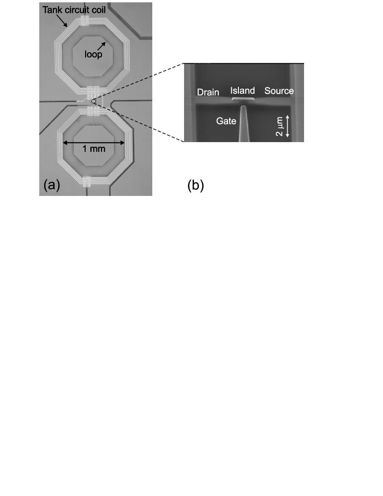
The Bloch transistor is included in a double superconducting loop of octagon shape with an outer dimension of 1.0 mm (see Fig. 2). Such a gradiometer design improves the stability against homogeneous magnetic field noise. The total inductance value of such a loop nH was estimated using Mohan’s formula mohan . This value is sufficiently small in the sense that, firstly, the corresponding magnetic energy is rather large, i.e. meV and, secondly, the dimensionless screening parameter, i.e. , is small. The former relation ensures the suppression of flux fluctuations and fixes the phase across the transistor klus . The latter one ensures the required non-hysteretic operation regime in the case of a single-junction SQUID circuit hansma ; rifkin76 , as well as of the realistic qubit circuit having finite asymmetry in the critical currents of individual junctions zorin03 . Moreover, the total inductance of the closed loop circuit is determined mostly by the transistor Josephson inductance. This inductance is directly related to the local curvature of the surface taken for fixed zorin03 , i.e.
| (1) |
In our measurements of the circuit in the ground state the band index , so we introduce the notation .
The loop is coupled through the mutual inductance to the coil of a resonant tank circuit formed by the double octagon-shaped spiral inductor with total inductance H (see Fig. 2a) and the capacitance of the coaxial cable connecting the tank to the preamplifier. The bare resonance frequency of such a tank circuit with quality factor is MHz. Due to the coupling to the qubit, the effective inductance of the circuit is changed hansma ,
| (2) |
in a gate-charge and phase specific way. The resulting shift of the resonant frequency, is zorin03
| (3) |
Here, denotes the coupling coefficient which is determined by the arrangement of the inductively coupled conductors. The integrated on-chip design of our qubit allows close mutual arrangement of the loop and the coil and, therefore, rather large values of . The tank circuit is driven by a combined current signal, consisting of a dc part fixing the working point, and an rf component at the frequency close to .
The cold preamplifier is based on an AGILENT ATF-10136 GaAs field-effect transistor. The output of the preamplifier is connected by the coaxial cable to the room-temperature amplifier. The overall gain of this two-stage scheme is about 26 dB in the range of typical resonant frequencies up to 90 MHz. The amplified rf voltage across the tank is fed to a lock-in amplifier measuring both the amplitude and the phase shift relative to the reference rf signal.
II.2 Pre-characterization of Bloch transistors
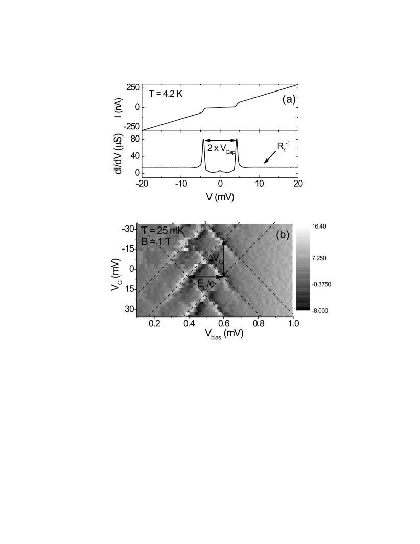
Embedding the Bloch transistors in a superconducting loop, unfortunately, renders its pre-characterization in a simple dc configuration impossible. To get nevertheless an estimate of the relevant parameters, i.e. the Josephson coupling energy and the charging energy , we characterized the similar stand-alone Bloch transistor structures fabricated from the same wafer, hence made from the same Nb/AlOx/Nb trilayer, and having the same dimensions. From - measurements at 4.2 K (shown in Fig. 3a) we extract the sum asymptotic resistance and the gap voltage . Resistance is assumed to equal twice the normal state resistance of one from two nominally identical junctions while the superconductor energy gap meV. Inserting these values into the Ambegaokar-Baratoff relation ambega , we estimate the critical current and, finally, , the Josephson coupling energy of one junction as listed in Table I. Note that values of 25 nA (wafer A) respectively 45 nA (wafer B) differ almost by a factor of 2. The radio-frequency measurements performed at 4.2 K with the single junctions inserted instead of the transistors in the similar loops (see Fig. 1), i.e. the rf-SQUID configuration, gave almost similar values for .
The values of were derived from the gate and bias voltage dependencies of the current of the stand-alone transistors at 20 mK and perpendicular magnetic field of up to 2 T. This magnetic field partially suppresses the superconductivity of the Nb electrodes and enhances the single-electron tunneling at small voltage bias pavolotsky . For the bias below the gap voltage we found the characteristic diamond-like pattern resulting from Josephson quasiparticle cycles tinkham ; the bias voltage period provides an estimate of the charging energy (see Fig. 3b and Table 1), while the gate voltage period mV gives the value of the gate capacitance, aF.
| T1 ( nm nm) | T2 ( nm nm) | |
| (eV) | 50 | 95 |
| (eV) | 80 | 45 |
| (nH) | 0.7 | 0.7 |
| (H) | 0.20 | 0.15 |
| (nH) | 4.6 | 3.8 |
| 0.42 | 0.39 | |
| (nA) | 3.9 | 17 |
| 0.008 | 0.036 | |
| (MHz) | 68.80 | 76.18 |
| 250 | 235 |
III Radio-frequency measurements
III.1 Resonance curves
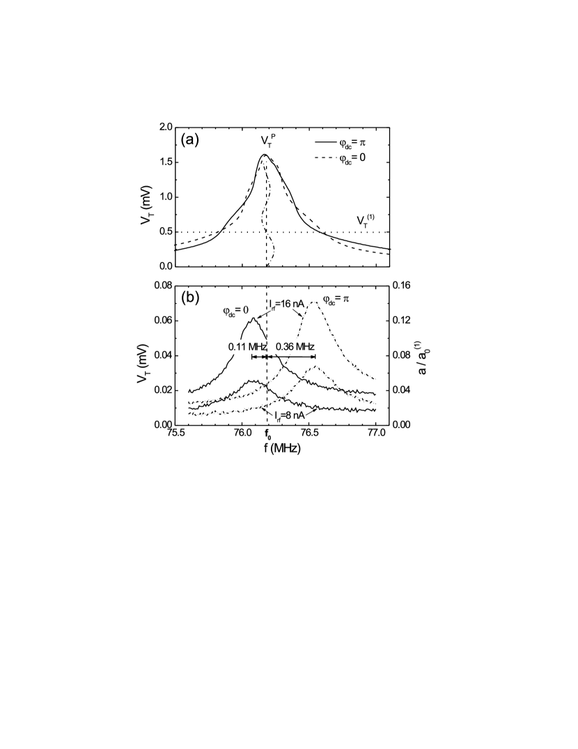
First, the resonance measurements of the Bloch transistors were performed in order to calibrate the rf oscillation amplitude of the phase, , with being proportional to the amplitude of the rf-flux oscillations in the loop, . The resonance curves for a moderate pumping amplitude are shown in Fig. 4a. The curves exhibit characteristic ”nodes” typical of rf-SQUIDs shnyrkov , where, at certain pumping levels, the sensitivity of the tank oscillation amplitude against the dc bias, i.e. the stationary Josephson phase difference , disappears. Assuming a sinusoidal current-phase relation (CPR), these ”nodes” are related to the amplitude-dependent resonant frequency for fixed given by the formula likha :
| (4) |
with denoting the first order Bessel-function. If equals one of the positive zeros () of function , the resonant frequency is no longer dependent on or on the dc bias current. The amplitude for the first node can be assigned to the respective value , thus providing calibration according to , where . The good agreement between the calculated -dependence (dash-dotted line in Fig. 4a) and the position of the nodes illustrates, that the transistor sample investigated behaves for rather large amplitudes approximately as an element with harmonic CPR. In other words, the contribution of higher harmonics in the CPR to the resulting resonance frequency is small.
For the small pumping levels, the resonance curve is shifted as a whole when changing the dc bias current, see Fig. 4b. In contrast to the situation for the large amplitude of oscillations, the non-harmonic shape of the CPR plays a crucial role here as expressed by Eq. (1) relating the local curvature of the band with the Josephson inductance. The frequency shift determined for the two opposite values of the external dc magnetic flux applied to the loop is no longer symmetric relative to the tank-circuit frequency since the reverse inductance producing this shift (see Eq. (3)) is not exactly proportional to here. This asymmetric splitting appears so clear in our experiment because of the rather large value of the product for sample T2 (cf. experiments on rf-SQUIDs with large values of this product in Ref. dmitrenko ). The minimum rf-excitation which allows us to work with a sufficiently high signal-to-noise ratio in our measurements corresponds to values .
For a sufficiently small value of the phase angle between the driving signal and the voltage oscillations is given by the formula
| (5) |
with the resonance frequency detuning resulting from the transistor’s Josephson inductance Eq. (3) and the relative shift of the operation frequency . The measurement of this angle for different values of the dc flux and gate charge at a sufficiently low temperature allows the curvature of the qubit ground state surface to be mapped.
III.2 Radio-frequency measurements at 4.2 K
As long as our samples are fabricated from Nb films having a critical temperature of about 9 K, they preserve the Josephson properties and can be measured at a temperature of K. Earlier, the rf measurements of transistors which comprise somewhat larger Nb junctions (with dimensions down to 300 nm by 300 nm) and are included in low-inductance loops were successfully carried out at 4.2 K by Il’ichev et al. imt1 . These samples showed a clear dependence of the phase angle on the applied dc flux and allowed the critical current of the junctions to be evaluated (about 55 nA). Due to the large capacitance of the island in these samples, the charging energy was small (about 4 eV, i.e. 50 mK) and the values of parameter were rather large (), so these transistors behaved classically at an operation temperature of 4.2 K, i.e. like two classical Josephson junctions connected in series. Surprisingly, our qubit samples with significant charging energy, i.e. , also exhibited a clear dependence of on the dc flux at this temperature.
Figure 5a shows the periodic dependencies - measured in the qubit sample T1 at 4.2 K (solid line) and 20 mK (dash-dotted line). For comparison, the corresponding curve (measured at 4.2 K) for the similar single Josephson junction included in the identical rf circuit is shown by a dash-double-dotted line. This plot demonstrates first the reduction of the critical current of the transistor in the ground state at mK () in comparison to a single junction. This is due to the charging effect of the island (see, for example, the experiments chargeexp ; chargeexp2 ). Secondly, one can see a further reduction of the critical current observed at the elevated temperature of 4.2 K.

Such behavior can be explained by a simple model which takes the mixed Bloch states at values of thermal energy into account which are comparable to the interband energies. In this case the observable supercurrent is found as the quantum-statistical averaging over the canonical ensemble,
| (6) |
where denotes the Hamiltonian of the total system including the electromagnetic environment in the thermal equilibrium at a temperature . In view of the small gate capacitance () and the small loop inductance (), the variables and can be regarded as classical parameters. The full expression for the supercurrent operator was derived in Ref. zorin03 . The diagonal matrix elements contributing to the expectation value entering in Eq. (6) are, therefore, equal to
| (7) |
where the effective Josephson coupling energy of the transistor is given by and is the operator of the transistor island’s phase (conjugate to the operator of the island’s charge). Note that the value (see the plots of this matrix element for in Ref. zorin96 ) also depends on the phase , because determines the ratio .
Note that due to the different signs of the term the supercurrent in the different Bloch bands , has usually inverted the phase dependencies (see the calculated curves in Fig. 5b as well as Fig. 3 in Ref. cpqb2 ). These anti-phase terms contribute with the corresponding Boltzmann’s factors to the observable value Eq. (6). Finally, the supercurrent value to be detected in the 4.2 K measurement is equal to
| (8) | |||||
The summation over takes into account both even and odd configurations of charge on the island. Both of these configurations are realized due to the unavoidable single electron tunneling at the elevated temperature. An analysis of Eq. (8) shows that taking into account the three lowest energy bands, i.e. choosing , is sufficient for an adequate description of our experiments with the given sample parameters and temperatures up to K. Then, higher bands () are sparsely populated and do not essentially contribute to . As a tendency, the dependence of on the gate charge practically vanishes as soon as higher bands get involved. The phase dependence becomes almost harmonic.
In Table 2 we compare the critical-current values calculated according to our model, , with those extracted from the measurements, , for both our transistor samples at 20 mK and 4.2 K. From the experimental data, we obtained the critical currents according to the relation
| (9) |
following from Eqs. (3) and (5). Here we introduce the value . For both temperatures considered here we find that the theoretical and the experimental critical currents are in good agreement. Moreover, the fact that does not differ for zero temperature and 20 mK, indicates, that measurements at the base temperature of the dilution refrigerator explore indeed the ground state.
| T1 | T2 | |
|---|---|---|
| at mK | 4.5 nA | 16 nA |
| at mK | 3.9 nA | 17 nA |
| at K | 0.9 nA | 4.3 nA |
| at K | 0.6 nA | 3.0 nA |
III.3 Mapping of the ground state
Figure 6 presents the phase dependence as a function of both external dc-flux (corresponding to the Josephson phase ) and the gate-voltage proportional to the quasi-charge for the samples T1 and T2. A nearly sinusoidal dependence of the phase on is to be seen which is modulated periodically by the applied gate voltage .
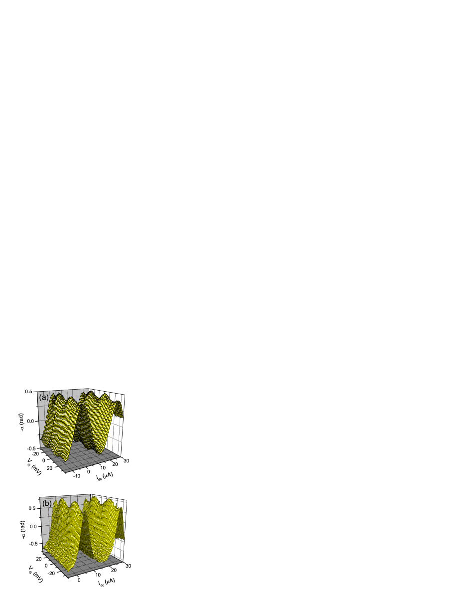
A closer look at Fig. 6 reveals that the amplitude of the oscillations of and, therefore, the critical current is smaller in T1 than in T2, as expected from the Ambegaokar-Baratoff-values of and also because of the smaller -ratio, due to the charging effects. The nominal values differ by less than a factor of 2, whereas the critical currents differ by more than a factor of 4. Related to that, the dc-bias dependence of is closer to the sinusoidal one for sample T1 having the smaller value of Zorin3 .
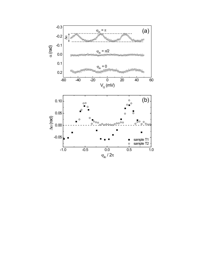
Gate-modulation curves of sample T1 (low -ratio) for different values are displayed in Fig. 7a. We find a periodic gate-modulation curve with a modulation depth of 0.05 rad for and of 0.09 rad for , whereas for , the gate charge sensitivity disappears almost completely. The gate-dependence period is roughly 29 mV for both samples and complies with the value found for the stand-alone test transistor shown in Fig. 3b. The gate oscillations are -periodic, since the periodicity does not change when applying a magnetic field of 2 T that is sufficient to cause intensive quasiparticle tunneling pavolotsky .
One should note that the gate modulation appears for sample T1 over the whole range of phase , hence allowing efficient qubit control over the whole flux bias range. On the other hand, for sample T2 () the modulation depth is non-zero only in the vicinity of the point (cf. Ref. imt2 , where this range was notably smaller) and almost zero for the rest of the flux-bias range, see Fig. 7b.
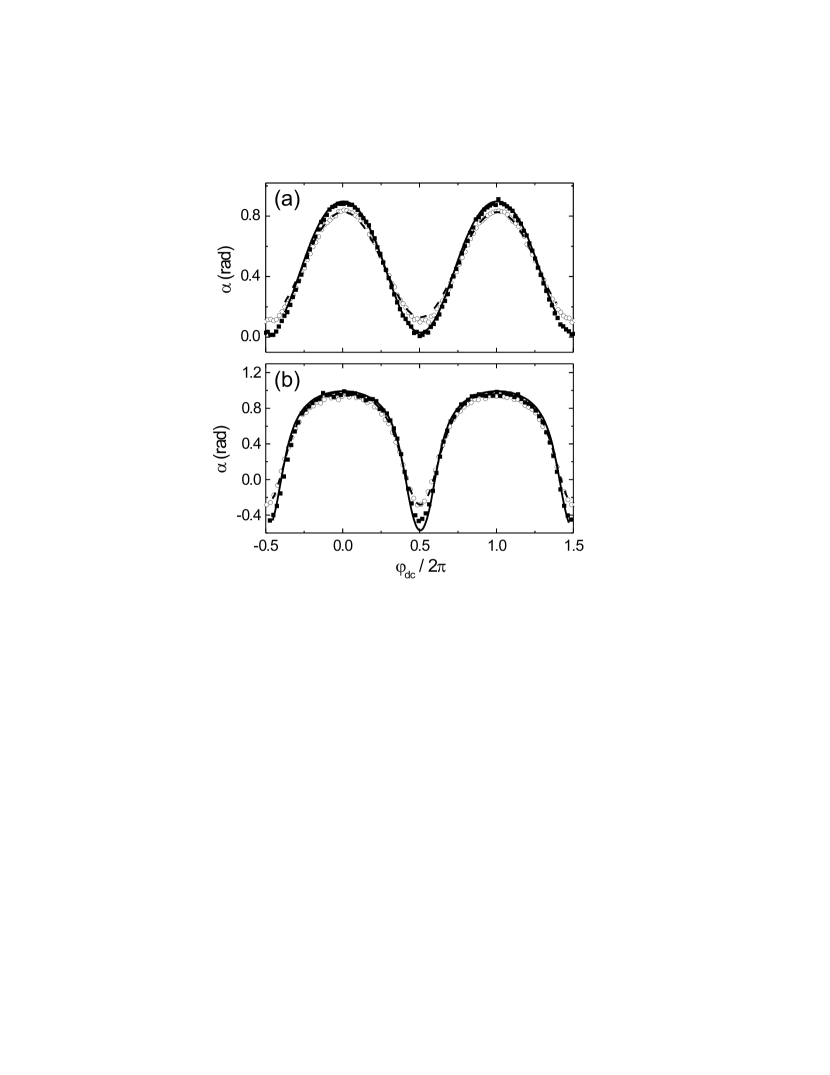
The surface plots of the phase shift presented in Fig. 6 should reflect the dependence of the local curvature of the ground-states energy on and (see Eq. 1). However, because of the finite amplitude of the oscillations, , of phase these surfaces yield the values of curvature averaged over the finite interval. Such averaging of the reverse Josephson inductance is described by the integral
| (10) |
This expression makes it possible to compare the obtained experimental data with the corresponding dependencies following from the theory, taking into account the local curvature of the ground state energy and the finite amplitude of the phase oscillations. By inserting the known parameters , , , , and into Eqs. (3), (5) and (10), we calculate the dc bias modulation curves for arbitrary charge on the transistor gate. The curves for and are shown in Fig. 8. These curves, which are based on input data partly deduced from the dc measurements described in Sec. II, agree well with the primary data from the rf experiments.
IV Conclusion
The radio-frequency impedance measurements of the charge-phase qubit samples with balanced Josephson coupling to Coulomb charging energy ratio clearly demonstrated the dependence of the curvature of the ground state energy on the control charge and phase in a wide range. The shape of the Josephson inductance surface of the transistor is well described by the Bloch band theory.
An advantage of our Nb-technology is, that we were able to characterize our qubit system at a temperature of K. In our investigation we found that the Josephson critical current of the tunnel junctions forming the qubit is scaled with their size, almost approaching the nominal Ambegaokar-Baratoff value. The availability of sub-0.1 m niobium-based Josephson junctions was extremely helpful as it offered the valuable new possibility of studying the influence of thermal fluctuations in an extended temperature range without increasing the cryogenic efforts. The experimental results obtained at the large temperature can be interpreted within a simple quantum-statistical model of the Bloch transistor.
Although the measured qubit samples T1 and T2 had a charging energy of the island (equal to 80 eV and 45 eV, respectively) much smaller than the value of the Nb energy gap, 1 meV, this relation did not ensure the desired suppression of the quasiparticle tunneling tuominen . As result, instead of the 2e-, the 1e-periodic dependence of the qubit Josephson inductance on the gate charge was observed. Such behaviour of the stand-alone Nb transistor samples was also observed in earlier measurements performed in dc configuration, see Ref. dolata05 and references therein. As was suggested in Ref. dolata05 , this behavior is most probably due to possible intragap energy states formed in Nb/AlOx/Nb tunnel barriers or due to non-equilibrium quasi-particles in the outer electrodes of the transistors chargeexp ; chargeexp3 . Therefore, further improvement of the Nb technology of fabrication is required. On the other hand, the given Nb qubit samples can still operate in the ”magic” points corresponding to the value of the control charge q = 0. The question as to the rate of the quasiparticle tunneling in the excited state, presenting the most critical mechanism of the qubit relaxation zorin03 , deserves a special study.
Acknowledgements.
We wish to thank H.-P. Duda and R. Harke for valuable technical assistance and I. Novikov for useful comments on the manuscript. As well, we would like to acknowledge Th. Weimann and P. Hinze for their support with the electron-beam writer and B. Egeling and R. Wendisch for their support in the PECVD and CMP processes. This work was supported by the European Union (projects SQUBIT-2 and EuroSQIP).References
- (1) Y. Makhlin, G. Schön and A. Shnirman, Rev. Mod. Phys. 73, 357 (2001).
- (2) D. Vion, A. Aassime, A. Cottet, P. Joyez, H. Pothier, C. Urbina, D. Esteve and M. H. Devoret, Science 296, 886 (2002).
- (3) V. Bouchiat, D. Vion, P. Joyez, D. Esteve, M. Devoret, Physica Scripta T76, 165 (1998).
- (4) D. V. Averin and K. K. Likharev, in Mesoscopic Phenomena in Solids, edited by B. L. Altshuler, P. A. Lee, and R. A. Webb (Elsevier, Amsterdam, 1991), p.175.
- (5) A. B. Zorin, Physica C 368, 284 (2002).
- (6) K. K. Likharev and A. B. Zorin, J. Low Temp. Phys. 59, 697 (1985); D. V. Averin, A. B. Zorin, and K. K. Likharev, Sov. Phys. JETP 88, 697 (1985).
- (7) A. B. Zorin, Phys. Rev. Lett. 76, 4408 (1996).
- (8) R. Rifkin and B. S. Deaver, Jr., Phys. Rev. B 13, 3894 (1976).
- (9) A. B. Zorin, JETP 98, 1250 (2004).
- (10) D. Born, V. I. Shnyrkov, W. Krech, Th. Wagner, E. Il’ichev, M. Grajcar, U. Hübner and H.-G. Meyer, Phys. Rev. B 70, 180501(R) (2004).
- (11) R. Dolata, H. Scherer, A. B. Zorin, and J. Niemeyer, J. Appl. Phys. 97, 054501 (2005).
- (12) For the parameter range discussed here, the qubit transition frequency is of the order of 10 GHz in the optimum ”magic” points of operation cpqb1 ; zorin03 , which is technically still convenient from the point of view of driving the qubit by microwave pulses.
- (13) S. S. Mohan, M. del Mar Hershenson, S. P. Boyd, and T. H. Lee, IEEE Trans. on Solid-State Circuits 34, 1419 (1999).
- (14) V. A. Khlus and I. O. Kulik, Sov. Tech. Phys. 20, 283 (1975).
- (15) P. K. Hansma, J. Appl. Phys. 44, 4191 (1973).
- (16) V. Ambegaokar and A. Baratoff, Phys. Rev. Lett. 10, 486 (1963).
- (17) A. B. Pavolotsky, T. Weimann, H. Scherer, V. A. Krupenin, J. Niemeyer and A. B. Zorin, J. Vac. Sci. Technol. B 17, 230 (1999).
- (18) M. T. Tuominen, J. M. Hergenrother, T. S. Tighe, and M. Tinkham, IEEE Trans. Appl. Spercond. 3, 1972 (1993).
- (19) V. I. Shnyrkov, V. A. Khlus and G. M. Tsoi, J. Low Temp. Phys. 39, 477 (1980).
- (20) K. K. Likharev, Dynamics of Josephson Junctions and Circuits (Gordon and Breach, New York, 1986), Ch. 14.
- (21) I. M. Dmitrenko, G. M. Tsoi, V. I. Shnyrkov, and V. V. Kartsovnik, J. Low Temp. Phys. 49, 417 (1982).
- (22) E. Il’ichev, V. Zakosarenko, L. Fritzsch, R. Stolz, H. E. Hoenig, H.-G. Meyer, M. Götz, A. B. Zorin, V. V. Khanin, A. B. Pavolotsky, and J. Niemeyer, Rev. Sci. Instrum. 72, 1882 (2001).
- (23) P. Joyez, P. Lafarge, A. Filipe, D. Esteve, and M. H. Devoret, Phys. Rev. Lett. 72, 2458 (1994).
- (24) T. M. Eiles and J. M. Martinis, Phys.Rev. B 50, 627(R) (1994).
- (25) A. B. Zorin, IEEE Trans. Instrum. and Meas. 46, 299 (1997).
- (26) M.T. Tuominen, J.M. Hergenrother, T.S. Tighe and M. Tinkham, Phys. Rev. Lett. 69, 1997 (1992).
- (27) J. Aumentado, M. W. Keller, J. M. Martinis, and M. H. Devoret, Phys. Rev. Lett. 92, 066802 (2004).