Fast Resonance Frequency Modulation in Superconducting Stripline Resonator
Abstract
Fast resonance frequency modulation of a superconducting stripline resonator is investigated. The experiments are performed using a novel device which integrates a hot electron detector (HED) into a superconducting stripline ring resonator. Frequency modulation is demonstrated by both applying dc current or voltage to the HED, and by applying optical illumination, with modulation frequencies of up to 4.2GHz. Potential applications for such a device are in telecommunication, quantum cryptography and biofluorescence.
Index Terms:
Parametric excitation, superconducting ring resonator, hot-electron detector, optoelectronics, NbN.I Introduction
Resonance parametric amplifiers are characterized by very low noise, high gain, and phase sensitive amplification. Parametric resonance in superconducting resonators [1] may allow some intriguing applications such as quantum squeezing[2], quantum non-demolition measurements [3], photon creation by the so-called dynamical Casimir effect[4], and more.
Parametric excitation occurs when the resonance frequency of an oscillator varies in time. The first parametric resonance occurs when the excitation is performed periodically at twice the resonance frequency , namely [5]. The system’s response to such an excitation depends on the dimensionless parameter , where is the quality factor of the resonator. When the system is said to be in the subthreshold regime, while above threshold, when the system breaks into oscillation. Achieving parametric gain where requires that the shift in the resonance frequency exceeds the width of its peak [6].
The frequency modulation mechanism, we employ here, is based on changing the boundary conditions of a superconducting resonator. This is done by switching a small section of the resonator to a normal state by using optical illumination. The switching time in superconductors is usually limited by the relaxation process of high-energy quasi-particles, also called ’hot-electrons’, giving their energy to the lattice, and recombining to form Cooper pairs. Recent experiments with photodetectors, based on a thin layer of superconducting Niobium-Nitride (NbN), have demonstrated an intrinsic switching time on the order of and a counting rate exceeding (see [7] and references therein). Resonance frequency shift by optical radiation [8], [9], [10], or high-energy particles [11], [12] (for which the required condition has been achieved) was demonstrated, though no periodic modulation was reported. Resonance frequency tuning [13] and switching [14] as well as optical and microwave signal mixing [15], [16] were demonstrated in normal-conducting GaAs microstrip ring resonators.
In this paper we show experimentally, that resonance frequency modulation, at twice the resonance frequency, is within reach using superconducting microwave resonators. Furthermore, the parametric gain threshold conditions, namely is demonstrated in a continuous wave (CW) measurement. The experiments are performed using a novel device, that integrates a HED into a superconducting ring resonator. The HED is used as an optically tuned, lumped element, that changes the boundary conditions of the resonator [17], and thus manipulates its resonance frequencies.
In the following section we describe the circuit design and fabrication process. The results section starts with the HED response to applied dc voltage and current, and the resulting effect on the resonance frequencies. These results are followed by a comparison with a theoretical model. Afterwards, the effect of CW and modulated infrared (IR) light on the resonance frequency is described, and fast optical modulation of the resonance frequency is demonstrated.
II Circuit Design and Fabrication
II-A Circuit Design
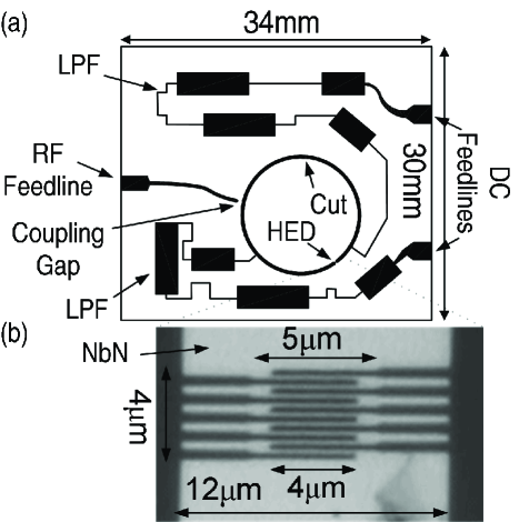
The circuit layout is illustrated in Fig. 1(a). The device is made of thick NbN stripline, fabricated on a sapphire wafer, with dimensions of The design integrates three components. The first is a superconducting ring resonator and its feedline. Ring configuration is a symmetric and compact geometry, which is generally suitable for applications, which require resonance tuning [13]. The first few resonance frequencies are designed for the S&C bands . The resonator is weakly coupled to its feedline, where the coupling gap is . The stripline width is set to , to obtain a characteristic impedance of
The second component is a HED, which is monolithically integrated into the ring structure. Its angular location, relative to the feedline coupling location, maximizes the RF current amplitude flowing through it, and thus maximizes its coupling to the resonator. The HED, shown in Fig. 1(b), has a meander structure, consists of nine NbN superconducting strips. Each strip has a characteristic area of and the strips are separated one from another by approximately [18].
The HED operating point is maintained by applying dc bias. The dc bias lines, forming the third component, are designed as two superconducting on-chip low-pass filters (LPF) with a cut-off frequency of . As this frequency is lower than the fundamental resonance frequency of the resonator, the intrinsic fields of the resonator are not appreciably perturbed. A cut of is made in the perimeter of the resonator, to force the dc bias current flow through the HED.
The device, which is top covered by a bare sapphire substrate, is housed in a gold plated Faraday package made of Oxygen Free High Conductivity (OFHC) Copper. Superconducting Niobium ground planes are dc-magnetron sputtered on the inner covers of the package. RF power is fed using a SMA launcher, coupled to the feedline. A dc bias is fed through two -LPFs, screwed to the package, having a cut-off frequency of . IR laser light is guided to the device by a fiber optic cable. A through hole of in diameter, is drilled in the Faraday package, and a fiber optic connector affixes the tip of the fiber cable at approximately above the HED.
II-B Fabrication Process
The fabrication process starts with a thorough pre-cleaning of the sapphire wafer in solvents. We have experienced that the commonly employed process of piranha followed by RCA cleaning substantially reduces the NbN adhesion to the Sapphire wafer. In the next step, thick gold pads are thermally evaporated through a mechanical mask to form the dc contact pads. The mask partially shadows the evaporation and thus the pads’ perimeters are smoothed. Epitaxy, thick, NbN film is then deposited at using a dc-magnetron sputtering system [19]. Sputtering parameters are summarized in table I and the process itself is further detailed in [20]. Next, an AlN layer of thickness is in-situ sputtered in N2 atmosphere at a temperature smaller than . This layer protects the vulnerable NbN layer during the following fabrication processes and restrain degradation [21]. It has also a functional role, as at cryogenic temperatures, it serves as a thermal conducting layer, which enhances the cooling of the NbN layer. In the next step, the HED meander stripline is patterned using electron beam lithography (EBL). The deposition of a thick PMMA 950K layer is followed by EBL with the following parameters: kVpA, and nC/cm, corresponding to acceleration voltage, emission current, and line dose respectively. Afterwards, the AlN layer is directly etched through the PMMA mask using ion milling. The remaining AlN layer serves as a mask for the sequential etching of the NbN layer, using low power reactive ion etching (RIE) in SF6 environment [22]. The remaining PMMA is removed by NMP. The last fabrication step is the patterning of the resonator and the LPFs features. This is achieved by using standard photolithography process. The photoresist development process (employing AZ-326 photoresist developer), also wet etches the AlN layer, while the remaining layer is again used as a mask for the RIE etching of the NbN film.
| Process parameter | NbN | AlN |
|---|---|---|
| Partial flow ratios (Ar,N2) | (87.5%,12.5%) | (0%,100%) |
| Base temperature | ||
| Base pressure | torr | torr |
| Work pressure | torr | torr |
| Discharge current | ||
| Discharge voltage | ||
| Deposition rate | sec | sec |
| Thickness () | ||
| Target-substrate distance |
III Experimental and Numerical Results
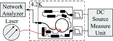
All measurements presented in this paper are carried out in a fully immersed sample in liquid helium (). The experimental setup, used for reflection measurements, is schematically depicted in Fig. 2. The samples’s RF feedline is connected to a vector network analyzer using a semi-rigid coax cable. The dc feedlines are connected to a dc source-measure unit using 4-probe wiring. The laser source has a wavelength of .
III-A DC I-V Measurements
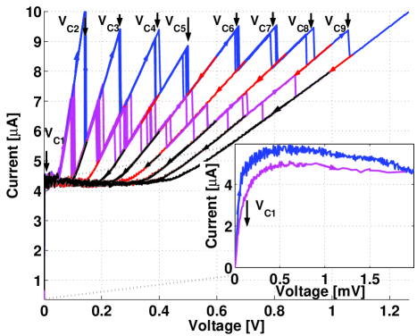
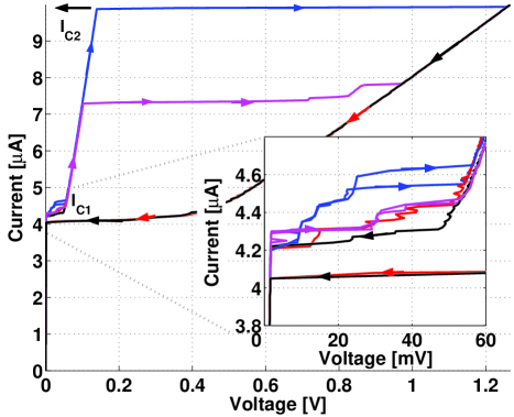
The basic I-V characteristics of the HED meander stripline, shown in Fig 3, exhibit a highly complex hysteretic behavior. Panel 3(a) plots nine current measurements, obtained while increasing the applied voltage (blue), one on top of the other, where each measurement starts at zero voltage and ends at a different maximum voltage, slightly above the voltages depicted in the figure. The corresponding nine current measurements, obtained while decreasing the applied voltage are also plotted (red). The magenta and black curves correspond to similar measurements, taken while the HED is being illuminated. The measurements for low applied voltages and currents are enlarged in the insets of Fig 3(a) and (b) respectively, where the finite resistance is due to the contacts.
At panel 3(a), nine, clearly distinguished, abrupt jumps in the measured current are noticed. The number of current jumps corresponds to the number of stripline sections that compose the meander shape of the HED. Each jump is the result of a large increase in the HED resistance due to a transition of one section from the superconducting state to the normal one. This behavior is typical for a superconducting microbridge and is caused by the formation of a hotspot in the bridge area [23]. Each critical voltage varies, in general, between different scans, indicating thus, the stochastic nature of the transitions between bistable states. The fluctuation in between different scans, characterizes the lifetime of the pre-jump metastable states of the system. The increase in at high voltages indicates a decrease in the lifetime of metastable states because of larger temperature fluctuations. The combined results of the increasing and decreasing applied voltage measurements show that large hysteresis is present at all current jumps except for the first one. This observation indicates, that only one section at a time can be biased into subcritical conditions. Furthermore, only the section responsible for the first jump, at , doesn’t suffer form hysteresis and thus can repetitively respond to radiation. Probably, the cause for this discretization of the critical current is the non-uniformity in the meander shape of the HED [23], [24]. Our finding clearly shows that the non-uniformity may substantially reduces the effective area of the HED, up to a fraction of of its printed area.
The same measurements are repeated while constantly illuminating the HED with approximately IR laser. In these measurements the current jumps occur at lower applied voltages, . In addition, are substantially widened. Although the decrease in the critical voltage values can be explained by local heating due to the IR illumination, the increase in , especially at low voltages, imply that photon absorptions cause discrete events that considerably increase the instability of the HED.
Panel 3(b) shows voltage measurements, obtained while increasing the applied current, with (magenta) and without (blue) IR illumination, and while decreasing the applied current, with (black) and without (red) IR illumination. Two abrupt voltage jumps occur at distinguishable critical currents of and . IR illumination has a negligible measured effect on and a strong effect on values. All voltage jumps suffer from hysteresis and therefore current bias is an unsuitable method for repetitive radiation detection.
 (a)
(a)
|
 (b)
(b)
|
III-B DC I-V Effect on the Resonance Lineshape
Fig. 4 shows several measurements as a function of frequency, in the vicinity of the second resonance mode, for various HED resistance values. For clarity, the resonance curves are vertically shifted upwards, for increasing resistance values. The measurements are obtained while applying variable voltage , and the resistance is measured simultaneously with the data using standard 4-probe technique. The RF input power is set to dBm, where the resonator is in the linear regime [25]. The inset of Fig. 4 plots the measured HED resistance as a function of .
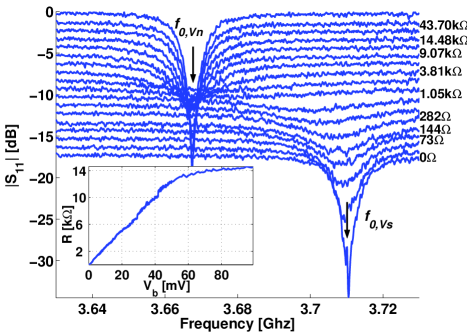
The dependence of the resonance characteristics on the HED resistance can be described as followed. At zero applied voltage the resonance frequency is At very low voltages, as the HED is biased far below critical conditions, its resistance is negligible and its influence on the resonance curve as well. As the resistance increases, the resonance frequency slightly red shifts, and more important, the Q-factor is significantly reduced due to dissipation in the HED. This behavior continues up to a point, at where the resonance curve can be hardly detected. When increasing the resistance beyond that point the trend of the Q-factor changes, the dissipation decreases, and the resonance curve reemerges at a new resonance frequency, , red shifted by approximately relative to its original value. The new resonance Q-factor has a value similar to the original one. When further increasing the resistance, the trend of the Q-factor continues but no additional resonance shift occurs. The behavior of the Q-factor suggests that as increases, the RF current amplitude of the resonance mode in the HED is reduced, due to current redistribution, and thus the total power dissipation decreases.
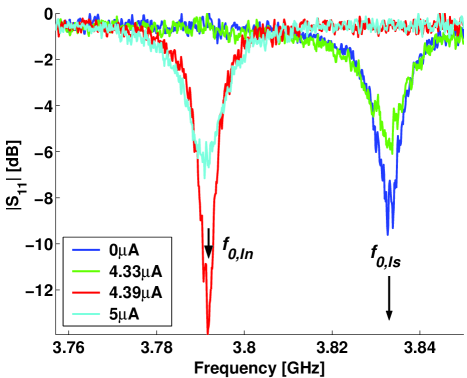
Similar behavior, with one major exception, can be observed under applied current, as shown in Fig 5. The blue, green, red, and cyan curves are taken with subcritical , , and over critical , applied currents, respectively, where is the current at which a first jump in the measured voltage occurs. There are two well defined resonance frequencies, , and which corresponds to applied currents below, and above respectively. , and slightly differ from , and as the two measurements were taken at different thermal cooldown cycles. Low Q-factor curves are absent from this measurement because under applied current, the HED can not be biased into intermediate resistance values. At bias currents below the HED has low resistance, which only slightly increases as the current approaches . As a result, no resonance shift occurs, and only the Q-factor slightly reduces as the current increases. This behavior changes abruptly once the HED resistance crosses a rather low, critical value, . A self-sustained hotspot is generated [23], quickly expends, and the HED becomes resistive. is the bias current at which is obtained. This thermal runaway causes an abrupt red shift of in the resonance frequency. Further increase of the bias current beyond increases the power dissipation and heat generation in the HED. This increases the local temperature and dissipation near the HED, and thus causes Q-factor reduction.
III-C Resonance Frequency Shift Modeling
To account for our results we calculate the resonance characteristics of our device, as a function of HED resistance.
As shown in Fig. 6, the ring resonator is modeled as a straight transmission line, extending in the directions. The HED is represented by a lumped discontinuity, , connecting points together, where is the resistance, is the angular frequency, and is the total inductance of the meander shape of the HED. The transmission line has a cut at point The couplings to the RF and dc feedlines are neglected.
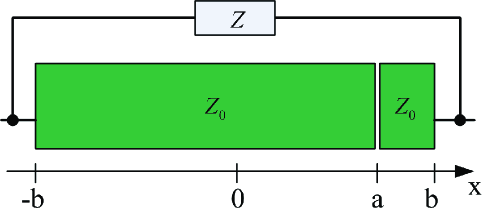
The voltage along the resonator’s transmission line is given by a standing waves expression of the form [26]
where is the propagation constant along the transmission line, is the frequency, is the relative dielectric constant, and is the speed of light in vacuum.
The current is given by where is the characteristic impedance of the line. By applying the following boundary conditions: , and we easily derive a boundary condition equation which yields the complex resonance frequencies of the resonator.
A phase transition of from superconducting to normal state simultaneously causes changes in its resistive, , and inductive, parts. Both changes contribute to a resonance shift in the same direction. For a very thin superconducting films resulting in Three fitting parameters are used in the model. Best fit results are obtained for and , which leads to nH for the second resonance mode. in the superconducting state, and thus negligible. The characteristic impedance value is in a very good agreement with the designed value of 50 The calculated inductance of the meander line at without any applied current is nH [27], but this value is strongly dependant on temperature and current density, so the fit parameter value is in reasonable agreement with the calculated one [27],[28].
Table II summarizes the first three solutions of the boundary condition equation for the two extreme cases of and . Comparing these results to the measured results (taken at two different cooldown cycles), also summarized in table II, shows a good agreement, especially for the second and third modes, for which the resonator is designed.
| Numerical Results | Experimental Results | |||||
|---|---|---|---|---|---|---|
| [MHz] | ||||||
| 1 | 1.913 | 1.873 | 39.8 | 1.59 | 1.58 | 10 |
| 2 | 3.791 | 3.747 | 43.7 | 3.874, 3.711 | 3.829, 3.668 | 45, 43 |
| 3 | 5.654 | 5.62 | 34.1 | 5.634, 5.38 | 5.608, 5.35 | 26, 30 |
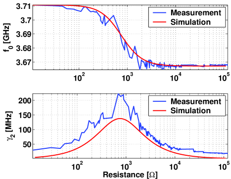
Fig. 7 shows the second resonance characteristics, resonance frequency and unloaded damping rate [2], of the experimental data (blue) and the numerically calculated data (red). The rate is extracted from the data plotted in Fig. 4 using the method presented in the appendix. The upper subplot shows the resonance frequency as a function of The calculated resonance frequency, at zero resistance, is , which equals the mean value of the resonance frequency measured at different cooldown cycles. In this subplot, the calculated data is corrected by to overlap between the first calculated and measured point. Both curves show the same dependence on The lower subplot shows the unloaded damping rate as a function of . Also in this case, a good agreement with the experiment is obtained, and as expected, the measured damping rate exceeds the calculated one, due to losses, which are not taken into account in the model.
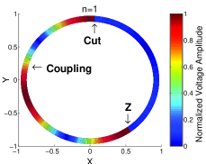
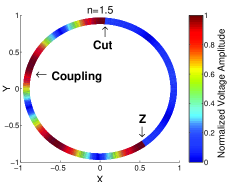
The coupling between the different modes and the HED can be characterized by the current amplitude through the HED. The model predicts normalized current amplitudes of and inside the lumped element, for the second and third modes respectively. This rather weak coupling is the result of the rather high kinetic inductance of the HED. To estimate the coupling of modes two and three to the feedline [29], we show in Fig. 8 the normalized voltage amplitudes, as a function of the ring’s angular location. The calculated normalized voltage amplitudes, at the feedline coupling location, are and respectively. The voltage amplitudes distribution have, in general, a strong dependence on the resonance frequency, and hence on , but because of the rather small resonance shift, the voltage amplitudes at the coupling location change by less than .
 (a)
(a)
|
 (b)
(b)
|
III-D IR Illumination Effect on the Resonance Lineshape
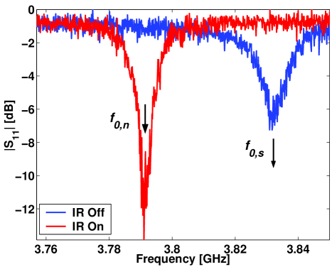
Fig. 9 plots measurements with (red) and without (blue) IR illumination. The effective IR illumination power, impinging on the HED, is approximately The RF input power is set to dBm and the HED is biased with a subcritical dc current of which only weakly influences the resonance curve. When the illumination is turned on, the resonance frequency abruptly shifts to a lower frequency. The new resonance lineshape has the same characteristics as the resonance lineshape measured without illumination under supercritical bias current of This measurement clearly shows that the resonance frequency is sensitive to IR illumination. The measured results in this experiment yield
III-E Fast Modulation of the Resonance Frequency
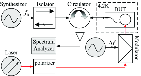
Fast modulation of the resonance frequency is performed using the experimental setup depicted in Fig 10. The resonator is excited by a CW pump signal, at frequency which coincides with the second resonance frequency. The optical signal is modulated at frequency , using a Mach-Zener modulator driven by a second CW signal, phase locked with the first one. The reflected power is mainly composed of three tones. One is the reflected pump signal at frequency . The other two are sidebands, produced by mixing the pump signal and the optical modulation signal, and are found at frequencies Occasionally, higher orders of the mixed signals are also detected. The amplified reflected power is measured using a spectrum analyzer, which tracks the tone. No dc bias is needed in this measurement as the RF probe signal also serves as a bias signal for the HED. This bias scheme has two major advantages over the dc bias scheme; first the RF pump bias signal has lower noise, as the and line noises are avoided. Second, the RF bias signal introduces a strong non-linear mechanism [25], [30], which will be discussed in a future publication [31], and produces a high internal gain of the induced optical signal.
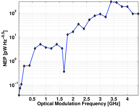
The device is not designed for radiation detection. Nevertheless, we find it useful to characterize the response to optical modulation by its noise equivalent power (NEP). Fig. 11 shows the NEP of the device for various optical modulation frequencies. Each NEP data point is derived out of several reflected power measurements in the vicinity of , where each measurement is performed with a different pump power, ranges between dBm and dBm. The best NEP is measured for a modulation frequency of and equals fW/. A rather low NEP of fW is measured for a modulation frequency of For this modulation frequency, coincides with the third resonance frequency of the resonator. Higher modulation frequencies than the ones presented in Fig. 11 are also observed, but the measured NEP is relatively poor, mainly due to the bandwidth limitations of the microwave components composing the experimental setup.
IV Discussion
Fast modulation of the resonance frequency is experimentally demonstrated. Furthermore, the parametric gain threshold condition is achieved in a CW measurement. The main problem, that currently prevents parametric gain to occur, is the relatively low photon flux that impinges the HED. Due to losses along the optical path, especially the expansion of the Gaussian beam from the tip of the fiber to the HED, the largest photon flux we currently manage to apply is approximately photons per modulation cycle, at twice the resonance frequency. Taking into account the effective area of the HED and its quantum efficiency [32] we estimate that the optical power flux is two orders of magnitude lower than the threshold power. Therefore parametric gain can not be achieved using the present device. Future devices will address this problem.
V Conclusion
We have reviewed the design, fabrication, and measurement results of our optically tunable resonator. Resonance frequency modulation frequency as high as is achieved, and a NEP of 38fW/ in the IR is measured. The parametric gain threshold condition is achieved in a CW measurement. Moreover, the results are shown to be in a good agreement with a theoretical modeling. The approach used in this device has a great potential of achieving a parametric amplification in superconducting resonators.
[Damping Rare Extraction]The universal expression for the reflection amplitude of a linear resonator near resonance is [2], [33]
| (1) |
where is the pump angular frequency , relative to the angular resonance frequency , is the coupling constant between the resonator and the feedline, and is the unloaded damping rate of the resonance. The damping rate is numerically extracted by expanding Eq. (1) to first order in ,
where is the value at the resonance frequency,
and is the slope of the imaginary part of
Note that the extraction of is less accurate for low Q-factor curves, and thus the calculated loss factor suffers from a rather large impreciseness at that regime.
References
- [1] N. V. Fomin, O. L. Shalaevand, and D. V. Shantsev, “Parametric resonance in superconducting micron-scale waveguides,” J. Appl. Phys., vol. 81, no. 12, pp. 8091–8096, Jun. 1997.
- [2] B. Yurke and E. Buks, “Performance of cavity-parametric amplifiers, employing kerr nonlinearites, in the presence of two-photon loss,” arXiv:quant-ph/0505018 v1, pp. 1–9, 2005.
- [3] B. C. Sanders and G. J. Milburn, “Complementarity in a quantum nondemolition measurement,” Phys. Rev. A, vol. 39, no. 2, pp. 694–702, Jan. 1989.
- [4] V. V. Dodonov and A. B. Klimov, “Generation and detection of photons in a cavity with a resonantly oscillating boundary,” Phys. Rev. A, vol. 53, no. 4, pp. 2664–2682, Apr. 1996.
- [5] L. Landau and E. Lifshits, Mechanics. New York: Oxford, 1976.
- [6] M. A. Golosovsky, H. J. Snortland, and M. R. Beasley, “Nonlinear microwave properties of superconducting Nb microstrip resonators,” Phys. Rev. B, vol. 51, no. 10, pp. 6462–6469, 1995.
- [7] G. N. Goltsman, A. Korneev, I. Rubtsova, I. Milostnaya, G. Chulkova, O. Minaeva, K. Smirnov, B. Voronov, W. Sysz, A. Pearlman, A. Verevkin, and R. Sobolewski, “Ultrafast superconducting single-photon detectors for near-infrared-wavelength quantum communications,” Phys. Status Solidi C, vol. 2, no. 5, pp. 1480–1488, 2005.
- [8] S. Cho and C.-S. Son, “Modulation of the resonance frequency of superconducting microwave resonators,” IEEE Trans. Appl. Superconduct., vol. 13, no. 2, pp. 3659–3662, Jun. 2003.
- [9] ——, “Observation of bolometric optical response in superconducting microwave meander lines,” J. Appl. Phys., vol. 84, no. 10, pp. 5657–5661, Nov. 1998.
- [10] M. Tsindlekht, M. Golosovsky, H. Chayet, and D. Davidov, “Frequency modulation of the superconducting parallel-plate microwave resonator by laser irradiation,” Appl. Phys. Lett., vol. 65, no. 22, pp. 2875–2877, Nov. 1994.
- [11] P. K. Day, H. G. LeDuc, B. A. Mazin, A. Vayonakis, and J. Zmuidzinas, “A broadband superconducting detector suitable for use in large arrays,” Nature, vol. 425, pp. 817–821, Oct. 2003.
- [12] R. Wedenig, T. Niinikoski, P. Berglund, J. K. R. Inen, L. Costa, M. Valtonen, R. Linna, J. Salmi, H. SeppaK, and I. Suni, “Superconducting NbN microstrip detectors,” Nucl. Instrum. Methods Phys. Res. A, vol. 443, no. 3, pp. 646–663, Sep. 1999.
- [13] K. Chang, S. Martin, F. Wang, and J. L. Klein, “On the study of microstrip ring and varactor-tuned ring circuits,” IEEE Trans. Microwave Theory Tech., vol. MTT-35, no. 12, pp. 1733–1739, Dec. 1987.
- [14] T. S. Martin, F. Wang, and K. Chang, “Theoretical and experimental investigation of novel varactor-tuned switchable microstrip rmg resonator circuits,” IEEE Trans. Microwave Theory Tech., vol. 36, no. 12, pp. 1733–1739, Dec. 1988.
- [15] J.-C. Lee, H. F. Taylor, and K. Chang, “Degenerate parametric amplification in an optoelectronic GaAs CPW-to-slotline ring resonator,” IEEE Microwave Guided Wave Lett., vol. 7, no. 9, pp. 267–269, Sep. 1997.
- [16] G. K. Gopalakrishnan, B. W. Fairchild, C. L. Yeh, C.-S. Park, K. Chang, M. H. Weichold, and H. F. Taylor, “Experimental investigation of microwave-optoelectronic interactions in a microstrip ring resonator,” IEEE Trans. Microwave Theory Tech., vol. 39, no. 12, pp. 2052–2060, Dec. 1991.
- [17] D. Saeedkia, A. H. Majedi, S. Safavi-Naeini, and R. R. Mansour, “Frequency and time-varying scattering parameters of a photo-excited superconducting microbridge,” IEEE Microwave Wireless Compon. Lett., vol. 15, no. 8, pp. 510–512, Aug. 2005.
- [18] J. Zhang, W. Slysz, A. Verevkin, O. Okunev, G. Chulkova, A. Korneev, A. Lipatov, G. N. Goltsman, and R. Sobolewski, “Response time characterization of NbN superconducting single-photon detectors,” IEEE Trans. Appl. Superconduct., vol. 13, no. 2, pp. 180–183, Jun. 2003.
- [19] G. N. Goltsman, K. Smirnov, P. Kouminov, B. Voronov, N. Kaurova, V. Drakinsky, J. Zhang, A. Verevkin, and R. Sobolewski, “Fabrication of nanostructured superconducting single-photon detectors,” IEEE Trans. Appl. Superconduct., vol. 13, no. 2, pp. 192–195, Jun. 2003.
- [20] B. Abdo, E. Segev, O. Shtempluck, and E. Buks, “Observation of bifurcations and hysteresis in nonlinear NbN superconducting microwave resonators,” cond-mat/0501114 v2, 2005.
- [21] B. Delaeta, J.-C. Villegierb, W. Escoffierb, J.-L. Thomassinb, P. Feautriera, I. Wangc, P. Renaud-Goudc, and J.-P. Poizat, “Fabrication and characterization of ultra-thin NbN hot electron bolometer for near infrared single photon detection,” Nucl. Instr. and Meth. A, vol. 520, pp. 541–543, 2004.
- [22] A. Lichtenberger, D. Lea, and F. Lloyd, “Investigation of etching techniques for superconducting Nb/Al-Al2O3/Nb fabrication processes,” IEEE Trans. Appl. Superconduct., vol. 3, no. 1, pp. 2191–2196, Mar. 1993.
- [23] A. V. Gurevich and R. G. Mints, “Self-heating in normal metals and superconductors,” Rev. Mod. Phys., vol. 59, no. 4, pp. 941–999, Oct. 1987.
- [24] J. Zhang, W. Slysz, A. Pearlman, A. Verevkin, R. Sobolewski, O. Okunev, G. Chulkova, and G. N. Goltsman, “Time delay of resistive-state formation in superconducting stripes excited by single optical photons,” Phys. Rev. B, vol. 67, 132508, 2003.
- [25] B. Abdo, E. Segev, O. Shtempluck, and E. Buks, “Nonlinear dynamics in the resonance lineshape of NbN superconducting resonators,” cond-mat/0601146, 2006.
- [26] P. Gardner, D. K. Paul, and K. P. Tan, “Planar microstrip ring resonator filters,” Antennas for Personal Communication Systems, IEE Colloquium, pp. 6/1 – 6/6, Feb. 1994.
- [27] S. M. Anlage, H. J. Snortland, and M. R. Beasley, “A current controlled variable delay superconducting transmission line,” IEEE Trans. Magn., vol. 25, no. 2, pp. 1388–1391, Mar. 1989.
- [28] S. Cho, J.-C. Park, and C. Lee, “Current and temperature controlled variable inductance insuperconducting microstrip lines,” IEEE Trans. Appl. Superconduct., vol. 11, no. 1, pp. 3090–3093, Mar. 2001.
- [29] R. E. Collin, Foundations for Microwave Engineering, 2nd ed. New York: McGraw-Hill, 1992, pp. 538-541.
- [30] B. Abdo, E. Segev, O. Shtempluck, and E. Buks, “Intermodulation gain in nonlinear NbN superconducting microwave resonators,” Appl. Phys. Lett., vol. 88, no. 1, Jan. 2006, to be published.
- [31] E. Segev, B. Abdo, O. Shtempluck, and E. Buks, In preparation.
- [32] A. Korneev, P. Kouminov, V. Matvienko, G. Chulkova, K. Smirnov, B. Voronov, G. N. Goltsman, M. Currie, W. Lo, K. Wilsher, J. Zhang, W. Slysz, A. Pearlman, A. Verevkin, and R. Sobolewskic, “Sensitivity and gigahertz counting performance of NbN superconducting single-photon detectors,” Appl. Phys. Lett., vol. 84, no. 26, pp. 5338–5340, Jun. 2004.
- [33] B. Abdo, E. Segev, O. Shtempluck, and E. Buks, “Nonlinear coupling in Nb/NbN superconducting microwave resonators,” Jan 2005, arXiv:cond-mat/0501236 v1.
| Eran Segev-Arbel was born in Haifa, Israel in 1975. He received the B.Sc. degree in electrical engineering from the Technion–Israel Institute of Technology, Haifa, Israel, in 2003. He is currently working toward the M.Sc. in electrical engineering at the Technion. His research is focused on parametric gain in superconducting microwave resonators. |
| Baleegh Abdo (S’2002) was born in Haifa, Israel in 1979. He received the B.Sc. degree in computer engineering, in 2002, and the M.Sc. degree in electrical engineering in 2004, both from the Technion–Israel Institute of Technology, Haifa, Israel. Currently he is pursuing the Ph.D. degree in electrical engineering at the Technion. His graduate research interests are nonlinear effects in superconducting resonators in the microwave regime, resonator coupling and quantum computation. |
| Oleg Shtempluck was born in Moldova in 1949. He received the M.Sc. degree in electronic engineering from the physical department of Chernovtsy State University, Soviet Union, in 1978. His research concerned semiconductors and dielectrics. From 1983 to 1992, he was a team leader in the division of design engineering in Electronmash factory, and from 1992 to 1999 he worked as stamp and mould design engineer in Ikar company, both in Ukraine. Currently he is working as a laboratory engineer in Microelectronics Research Center, Technion- Israel Institute of Technology, Haifa, Israel. |
| Eyal Buks received the B.Sc. degree in mathematics and physics from the Tel-Aviv University, Tel-Aviv, Israel, in 1991 and the M.Sc. and Ph.D. degrees in physics from the Weizmann Institute of Science, Israel, in 1994 and 1998, respectively. His graduate work concentrated on interference and dephasing in mesoscopic systems. From 1998 to 2002, he worked at the California Institute of Technology (Caltech), Pasadena, as a Postdoctoral Scholar studying experimentally nanomachining devices. He is currently a Senior Lecturer at the Technion—Israel Institute of Technology, Haifa. His current research is focused on nanomachining and mesoscopic physics. |