Controllable junction with magnetic nanostructures
Abstract
We propose a novel Josephson device in which and states are controlled by an electrical current. In this system, the state appears in a superconductor/normal metal/superconductor junction due to the non-local spin accumulation in the normal metal which is induced by spin injection from a ferromagnetic electrode. Our proposal offers not only new possibilities for application of superconducting spin-electronic devices but also the in-depth understanding of the spin-dependent phenomena in magnetic nanostructures.
pacs:
74.50.+r, 74.45.+c, 85.25.CpNowadays spin-electronics is one of the central topics in condensed matter physics Maekawa1 ; Maekawa2 ; Zutic . There has been considerable interest in the spin injection, accumulation, transport, and detection in ferromagnet/normal metal (F/N) hybrid structures Johnson ; Jedema1 ; Jedema2 ; Otani ; Son ; Takahashi1 . Twenty years ago, Johnson and Silsbee demonstrated the spin injection and detection in a F/N/F structure for the first time Johnson . Recently, spin accumulation has been observed at room temperature in all-metallic spin-valve geometry consisting of a F/N/F junction by Jedema et al. Jedema1 . In their system, the spin-polarized bias current is applied at one F/N junction, and the voltage is measured at another F/N interface for the parallel (P) and antiparallel (AP) alignments of the F’s magnetizations. They have observed the difference of the non-local voltages between the P and AP alignments due to spin accumulation in N. Also in a F/I/N/I/F (I indicates an insulator) structure, a clear evidence of spin accumulation in N has been shown Jedema2 . In hybrid structures consisting of a ferromagnet and a superconductor (S), a suppression of the superconductivity due to spin accumulation in S has been studied theoretically and experimentally Takahashi2 ; Vasko ; Dong .
Furthermore, ferromagnetic Josephson (S/F/S) junctions have been studied actively in recent years Buzdin ; Demler ; Sellier ; Ryazanov ; Kontos ; Bauer . In the S/F/S junctions, the pair potential oscillates spatially due to the exchange interaction in F Buzdin ; Demler . When the pair potentials in two S’s take different sign, the direction of the Josephson current is reversed compared to that in ordinary Josephson junctions. This state is called the state in contrast with the state in ordinary Josephson junctions because the current-phase relation of the state is shifted by “” compared to that of the state. The observations of the state have been reported in various systems experimentally Sellier ; Ryazanov ; Kontos ; Bauer . The applications of the state to the quantum computing also have been proposed Yamashita1 ; Yamashita2 ; Ioffe . Another system to realize the state is a S/N/S junction with a voltage-control channel Baselmans1 ; Baselmans2 . In the system, the non-equilibrium electron distribution in N induced by the bias voltage plays an important role, and the sign reversal of the Josephson critical current as a function of the control voltage has been demonstrated Baselmans1 ; Baselmans2 .
In this paper, we propose a new Josephson device in which the and states are controlled electrically. In this device, spin accumulation is generated in a nonmagnetic metal by the spin-polarized bias current flowing into the nonmagnetic metal from a ferromagnet. In a metallic Josephson junction consisting of the spin accumulated nonmagnetic metal sandwiched by two superconductors, the state appears due to the spin split of the electrochemical potential in the nonmagnetic metal. The magnitude of spin accumulation is proportional to the value of the spin-polarized bias current, and therefore the state of the Josephson junction is controlled by the current. Our proposal leads to an in-depth understanding of the spin-dependent phenomena in magnetic nanostructures as well as new possibilities for the application of superconducting spin-electronic devices.
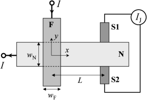
We consider a magnetic nanostructure with two superconductors as shown in Fig. 1. The device consists of a nonmagnetic metal N (the width , the thickness ) which is connected to a ferromagnetic metal F (the width , the thickness ) at and sandwiched by two superconductors S1, S2 located at . In this device, the electrode F plays a role as a spin-injector to the electrode N, and the S1/N/S2 junction is a metallic Josephson junction. The spin-diffusion length in N is much longer than the length in F Johnson ; Jedema1 ; Jedema2 ; Otani ; Takahashi1 , and we consider the structure with dimensions of which is a realistic geometry Jedema1 ; Jedema2 .
In the electrodes N and F, the electrical current with spin is expressed as
| (1) |
where and are the electrical conductivity and the electrochemical potential (ECP) for spin , respectively. Here ECP is defined as , where is the chemical potential of electrons with spin and is the electric potential. From the continuity equation for charge, , and that for spin, ( is the carrier density for spin ), we obtain Takahashi1 ; Son
| (2) | |||
| (3) |
where is the spin diffusion length with the diffusion constant ( and are the density of states and the diffusion constant for spin , respectively) and the scattering time of an electron ( is the scattering time of an electron from spin to ). In order to derive Eqs. (2) and (3), we take the relaxation-time approximation for the carrier density, , and use the relations and , where and are the carrier density deviation from equilibrium and the shift in the chemical potential from its equilibrium value for spin , respectively. In addition, the detailed balance equation is also used. We use the notations in N and () in F hereafter.
At the interface between N and F, the interfacial current flows due to the difference of ECPs in N and F: , where is the spin-dependent interfacial conductance. We define the interfacial charge and spin currents as and , respectively. The spin-flip effect at the interface is neglected for simplicity. In the electrode N with the thickness and the contact dimensions being much smaller than the spin-diffusion length (), varies only in the direction Takahashi1 . The charge and spin current densities in N, and , are derived from Eqs. (1)(3), and satisfy the continuity conditions at the interface: and , where is the cross-sectional area of N. From these conditions, we obtain ECP in N, , where for , for , and . In the electrode F, the spin split of ECP, , decays in the -direction because the thickness of F and the dimension of the interface are much larger than the spin-diffusion length in F () Takahashi1 . In a similar way to the case of N, ECP in F is obtained from the continuity conditions for charge and spin currents. ECP in F is expressed as , where and with the contact area , the voltage drop at the interface , and the polarization of the current in F, . The influence of the electrodes S1 and S2 on ECP in N may be neglected. When the superconducting gap in S1 and S2 is much larger than the spin split at , almost no quasiparticle is excited above the gap at low temperature. Therefore, the spin current does not flow into S1 and S2, and the behavior of ECP in N is not modified by the connection to the electrodes S1 and S2.
In order to obtain the relation between the bias current and the shift of ECP, , at the right side in N (), we substitute the obtained and for the expressions of and , and eliminate . As a result, we obtain the relation between and , and finally we get the relation between and as follows:
| (4) |
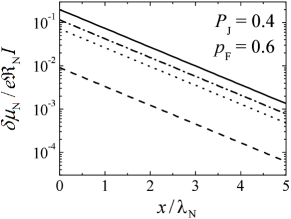
where ) and indicate the non-equilibrium resistances of N and F, respectively, is the interfacial resistance, and is the polarization of the interfacial current. When the F/N interface is the tunnel junction (), Eq. (4) reduces to a simple form . On the other hand, when the F/N junction is of metallic contact (), Eq. (4) becomes , where is a mismatch factor of the resistances in F and N. Figure 2 shows the spacial variation of both for the tunnel- and metallic-limit cases with and Maekawa1 ; Bass . As shown in this figure, in the case of the metallic contact, becomes larger with decreasing the resistance mismatch Takahashi1 .
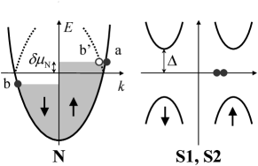
Next we consider how spin accumulation affects the Josephson current flowing through the S1/N/S2 junction located at (Fig. 1). In the metallic Josephson junction, the Andreev bound state plays a key role for the Josephson effect Sellier ; Andreev . The Andreev bound state is formed by a multiple Andreev reflection of an electron with the wave number and a hole with , respectively, where is the energy of the electron and hole measured from the Fermi energy . As shown in Fig. 3, when there is the spin split in N, a spin-up (-down) electron with the energy () is injected into S’s from N at low temperatures. The injected electron captures another electron with the energy () from the opposite spin band in order to form a Cooper pair in S’s. Therefore, a spin-up (-down) hole with energy () is reflected back to N (Andreev reflection Andreev ). In other words, the spin-up (-down) electron with and the spin-up (-down) hole with mainly contribute to the formation of a Cooper pair. Note that the values of the wave numbers and differ due to the spin split in contrast with the case of no spin split () in which .
The split corresponds to the exchange energy of a ferromagnet in a superconductor/ferromagnet/superconductor (S/F/S) Josephson junction as follows Buzdin ; Demler ; Sellier ; Ryazanov ; Kontos ; Bauer : In the S/F/S systems, Cooper pairs are formed by the Andreev reflection of spin- electrons with the wave number and holes with at the energy . In the case that the exchange interaction is much weaker than the Fermi energy (), the stable state ( or ) in the system depends on the dimensionless parameter , where is the thickness of F and is the Fermi wave number Sellier . At the system is in the state, and the first - transition occurs at , and then the system is in the state at Sellier . Because the value of is fixed in the S/F/S system, the and states change periodically with the period as a function of . As a result, the dependence of the Josephson critical current shows a cusp structure and the critical current becomes minimum at the - transition Kontos ; Sellier .
In analogy with the case of the S/F/S junction discussed above, when there is spin accumulation in N as shown in Fig. 3, the or state is realized in the S1/N/S2 junction depending on the parameter . In this case, the width is fixed, and the and states are controlled through the value of which is proportional to the bias current (see Eq. (4)). The N part of the system is in the non-equilibrium state by the spin current in contrast with F in the equilibrium state of the S/F/S junction. However, one can discuss the critical current in the non-equilibrium S1/N/S2 junction in the same way as the equilibrium S/F/S junction because the critical current is dominated by the energy of the quasiparticles in N, not by the flow of the current Baselmans1 ; Baselmans2 .
From the point of view of more detailed description, the free energy in the system is obtained by the summation of the energy of the Andreev bound states Yamashita1 . The bound state energy is calculated from the Bogoliubov-de Gennes equation BdG , and the free energy is minimum for the phase difference () for the () state. In the S1/N/S2 junction with no spin accumulation in N (), the bound states with the energy contribute to the free energy. On the other hand, when spin accumulation exists in N, the spin-up (-down) bound states with the energy () contribute to the free energy because ECP is shifted by () in N. The - transition occurs due to the shift of the energy region of the Andreev bound states which contribute to the free energy.
As an example, we consider the case that the F/N interface consists of a tunnel junction. The material parameters , , , , and , which lead to , are taken. The distance between F and S’s is taken to be . When no bias current is applied between F and N (), the S1/N/S2 junction is in the ordinary state because there is no spin split of ECP (). With increasing the bias current, the magnitude of the Josephson critical current decreases because the parameter increases due to the increase of the spin split. When the bias current reaches the value which induces the spin split at , the parameter and the first transition to the state from the state occurs (the values of and are taken AM ). As a result, the magnitude of the Josephson critical current takes its minimum at , and increases with increasing the bias current . When the bias current attains , the magnitude of the Josephson critical current becomes maximum because of , and decreases with increasing the bias current . For corresponding to , the second transition to the state from the state occurs.
Here we discuss the effect of spin accumulation on the superconducting gap Takahashi2 . The spin split at in N causes the split of ECP of S’s by near the S/N interfaces. The spin split in S’s decreases exponentially with the spin-diffusion length from the interface. In the superconductors, the superconducting gap is not suppressed by spin accumulation until exceeds the critical value of the spin split Takahashi2 . At low temperatures much lower than the superconducting critical temperature (), the critical value of the spin split is obtained as by solving the gap equation Takahashi2 , where is the superconducting gap for at . In the case discussed in the above paragraph, at the first - transition (). For example, for niobium Kittel , and therefore the superconducting gap is almost not affected by spin accumulation at the first - transition. When superconductors with the higher value of , e.g., ( 39 K) Nagamatsu or High- materials ( is several 10 K’s) Kittel , are used as the electrodes S1 and S2, the superconductivity is robust even at the second (, ) and higher - transitions.
In summary, we have proposed the novel Josephson device in which the and states are controlled electrically. The spin split of the electrochemical potential is induced in the electrode N by the spin-polarized bias current flowing from F to N. The state appears in the S1/N/S2 junction due to the non-local spin accumulation in N. Because the magnitude of spin accumulation is proportional to the value of the spin-polarized bias current, the and states of the Josephson junction are controlled by the current. Our proposal provides not only new possibilities for the application of superconducting spin-electronic devices but also the deeper understanding of the spin-dependent phenomena in the magnetic nanostructures.
We are grateful to M. Mori and G. Montambaux for fruitful discussion. T.Y. was supported by JSPS Research Fellowships for Young Scientists. This work was supported by NAREGI Nanoscience Project, Ministry of Education, Culture, Sports, Science and Technology (MEXT) of Japan, and by a Grant-in-Aid from MEXT and NEDO of Japan.
References
- (1) Spin Dependent Transport in Magnetic Nanostructures, edited by S. Maekawa and T. Shinjo (Taylor and Francis, London and New York, 2002).
- (2) Concepts in Spin Electronics, edited by S. Maekawa (Oxford Univ. Press, 2006).
- (3) I. uti, J. Fabian, and S. Das Sarma, Rev. Mod. Phys. 76, 323 (2004).
- (4) M. Johnson and R.H. Silsbee, Phys. Rev. Lett. 55, 1790 (1985); M. Johnson, ibid. 70, 2142 (1993).
- (5) F.J. Jedema, A.T. Filip, and B.J. van Wees, Nature (London) 410, 345 (2001).
- (6) F.J. Jedema et al., Nature (London) 416, 713 (2002).
- (7) Y. Otani et al., J. Magn. Magn. Mater. 239, 135 (2002); T. Kimura, J. Hamrle, and Y. Otani, Phys. Rev. B 72, 014461 (2005).
- (8) S. Takahashi and S. Maekawa, Phys. Rev. B 67, 052409 (2003).
- (9) P.C. van Son, H. van Kempen, and P. Wyder, Phys. Rev. Lett. 58, 2271 (1987).
- (10) S. Takahashi, H. Imamura, and S. Maekawa, Phys. Rev. Lett. 82, 3911 (1999).
- (11) V.A. Vas’ko et al., Phys. Rev. Lett. 78, 1134 (1997).
- (12) Z.W. Dong et al., Appl. Phys. Lett. 71, 1718 (1997).
- (13) A.I. Buzdin, L.N. Bulaevskii, and S.V. Panyukov, JETP Lett. 35, 178 (1982).
- (14) E.A. Demler, G.B. Arnold, M.R. Beasley, Phys. Rev. B 55, 15174 (1997).
- (15) V.V. Ryazanov et al., Phys. Rev. Lett. 86, 2427 (2001).
- (16) T. Kontos et al., Phys. Rev. Lett. 86, 304 (2001); ibid. 89, 137007 (2002).
- (17) H. Sellier et al., Phys. Rev. B 68, 054531 (2003).
- (18) A. Bauer et al., Phys. Rev. Lett. 92, 217001 (2004).
- (19) T. Yamashita et al., Phys. Rev. Lett. 95, 097001 (2005).
- (20) T. Yamashita, S. Takahashi, and S. Maekawa, cond-mat/0507199.
- (21) L.B. Ioffe et al., Nature (London) 398, 679 (1999); G. Blatter, V.B. Geshkenbein, and L.B. Ioffe, Phys. Rev. B 63, 174511 (2001).
- (22) J.J.A. Baselmans et al., Nature (London) 397, 43 (1999).
- (23) J.J.A. Baselmans et al., Phys. Rev. Lett. 89, 207002 (2002); J.J.A. Baselmans, B.J. van Wees, and T.M. Klapwijk, Phys. Rev. B 65, 224513 (2002).
- (24) J. Bass and W.P. Pratt Jr., J. Magn. Magn. Mater. 200, 274 (2000); J. Bass and W.P. Pratt Jr., Physica B 321, 1 (2002).
- (25) A.F. Andreev, Sov. Phys. JETP 19, 1228 (1964).
- (26) P.G. de Gennes, Superconductivity of Metals and Alloys (W. A. Benjamin, New York, 1966), chap. 5.
- (27) N. Ashcroft and N. Mermin, Solid State Physics (Saunders College Publishing, New York, 1976).
- (28) C. Kittel, Introduction to Solid State Physics (John Wiley & Sons, Inc., New York, 1996).
- (29) J. Nagamatsu et al., Nature (London) 410, 63 (2001).