Spintronics for electrical measurement of light polarization
Abstract
The helicity of a circularly polarized light beam may be determined by the spin direction of photo-excited electrons in a III-V semiconductor. We present a theoretical demonstration how the direction of the ensuing electron spin polarization may be determined by electrical means of two ferromagnet/semiconductor Schottky barriers. The proposed scheme allows for time-resolved detection of spin accumulation in small structures and may have a device application.
I Introduction
The ability to measure the circular polarization of light has greatly facilitated the progress of spintronics research in III-V semiconductor systems Wolf_Science00 in comparison with silicon whose conduction electrons are not optically active. The connection between spin orientation and light polarization in semiconductors is given by the angular momentum conservation rules. Optical_Orientation The spin polarization of the electrons in a III-V semiconductor, in the case of a current injection from a ferromagnetic metal, has been measured either by the circular polarization of light from a light emitting diode Fiederling_Nature99 ; Hanbicki_APL02 or by scanning Kerr spectroscopy in a lateral geometry. crooker The spin polarization has also been measured in the case of extraction current into the ferromagnet by Faraday rotation, epstein by scanning Kerr spectroscopy, crooker and by Hanle effect. stephens The determination of light polarization has, of course, a much broader application in information technology. The current principle of polarimetry is based on the methods of optics, relying on, for example, photoelastic modulators and beam splitter hipps or the different reflection intensities of polarized light. unlu The question is whether one can use for polarimetry the reversal of the roles between the ferromagnet/III-V semiconductor and the polarized light. The transmission from the semiconductor to the ferromagnet is spin-dependent ciuti1 and the spin dependence of the photocurrent passing through the junction indicates the sense of the circular polarization of the light exciting the electrons provided the contribution from the magnetic circular dichroism is removed. Steinmuller_PRB05 . Detection of a spin-dependent photocurrent has been recently reported in a p-n heterojunction junction held in magnetic field Kondo .
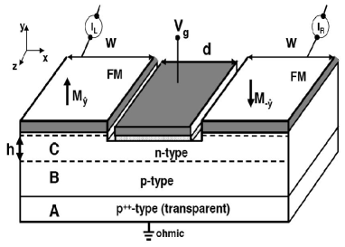
In this paper we analyze the time dependent response of the spin polarized electron transport after the absorption of polarized light. We choose a spintronics system configuration which may lead to detection of the helicity of a circularly polarized light beam as shown in Figure 1. It makes a direct use of the dependence between the magnetization of the contact and the spin polarized electrical current across the semiconductor/ferromagnet tunneling barrier. The beam excites spin-polarized electrons and holes below the stack. The electrons and holes are separated by the p-n junction. The electrons are swept upwards towards the gate and the electrodes. The photocurrent is split through two Schottky barriers with ferromagnets of opposite magnetizations. The different magnitudes of the split currents depend on whether the photo-excited electron spins are parallel or antiparallel to the magnets. The detection scheme takes advantage of the recent advances in the tunnel barrier fabrication either as a Schottky barrier Hanbicki_APL02 or separated by an oxide layer parkin which enable efficient transmission of spin currents at room temperature. For the potential practical applications, the monolithic spintronics system is portable and has a much smaller footprint than the currently available polarimeters. In addition, the phenomenon can be used to detect the amplitude of photo-excited spin accumulation in the semiconductor by a simple electrical measurement. The size of the spin accumulation region may be smaller than the spatial resolution of the scanning magneto-optical techniques (by Faraday or Kerr effects) limited by the wavelength of light.
In the next section we construct a system suitable for the electron spin response to polarized light stimulation. In section III we study the transport theory of the photo-excited electrons. We provide analytical expressions for the steady state case whose results are presented in section IV. In section V we study the time dependent analysis of the 2D spin diffusion equation. The results provide a complementary physical picture for the steady state case. We support the numerical simulations with a simplified picture from which one can achieve a deeper understanding of the dynamics. Conclusions are given in section VI.
II System requirements for detection of light polarization
A polarization detection scheme would depend on the correlation between the optical and the magnetic properties, which in turn would require the collinearity of the light propagation axis and the ferromagnet magnetization axes. This is simply the conservation of angular momentum when the spin quantization axis lies along the propagation direction of the polarized light. In terms of the axes labeled in Fig. 1, the collinear direction is along the -axis in which pinning of the magnetization out of plane may be realized by stacking alternate ferromagnetic and antiferromagnetic layers on top of each contact.garcia_out_of_plane The light can come from below, through the transparent substrate, in which case the thickness of the absorbing layer should not exceed the absorption depth. Alternatively, the light can come from above, and depending on the thicknesses of the contacts and the gate (see Fig. 1), the photocarriers can be generated everywhere in the semiconductors channel, or only under the gate.
The choice of the semiconductor materials is governed by the wavelength of the excitation light. In bulk semiconductors, the upper and lower bounds of the wavelength are set, respectively, by the threshold of band gap transitions and by the onset of transitions between the split-off valence band and the conduction band. For circularly polarized beam the degeneracy of the heavy and the light hole bands in bulk III-IV compounds leads to our assumption of optical excitation of both types of holes. In order to quantify the spin polarization the beam intensity is decomposed into two generating terms of photo-excited electrons and which correspond, respectively, to electrons with spin up and spin down. The resulting spin polarization is / where the sign depends on the light helicity. Optical_Orientation
The gate is essential to the stability of the system. It screens the in-plane electric field due to excess electrons in the channel by bringing “mirror” charges to the metal surface adjacent to the insulator. The screening is effective for a high aspect ratio between the channel length and the thickness of the insulating barrier separating it from the gate. Consequently, the system is electrostatically stable as in MOSFET devices and the transport along the axis connecting the ferromagnets may be assumed to be purely diffusive. The gate may have an additional role if the p-n junction of Fig. 1 is replaced by an alternate design with a unipolar doped structure. In this case the gate should be biased so that a charge accumulation (inversion) layer is formed if an n-doped (p-doped) semiconductor is used. The gate electric field in the semiconductor replaces the built-in field of the p-n junction in the function of sweeping the electrons into the conduction channel. Note that the electron gas in the conduction channel is 3D in the quantum character as we take the effective conduction channel thickness to exceed the electron de Broglie wavelength.
The scale of the system geometry is set by the spin diffusion length, about 1 m in GaAs at room temperature, which limits the travel distance of the spin-polarized electrons in the system. For high detection efficiency, the thickness of the conduction channel should be much less than the spin diffusion length. The width of the gate, which attracts the excited electrons to the conduction channel, must also be less than the diffusion length. Below we find the optimal width of each ferromagnetic contact to be less than the spin diffusion length. There is a corresponding important dependence of the efficiency of the lateral semiconductor spin valve on the width of the contacts in the planar geometry. Dery_contact In order to limit the spins to the active area, the pillar structure is designed to restrict the electrons under the ferromagnetic contacts or between them.
III Electron transport
The polarized beam creates non-equilibrium spin-dependent components of the density , for spin up or spin down. The resultant net spin density, , gives rise to spin accumulation in the channel. To simplify the following numerical procedures and in order to extract analytical expressions when possible we consider weak excitations. This means that the deviations from equilibrium, , are one or two orders of magnitude smaller than the free carrier concentration in the paramagnetic channel at equilibrium (). In this regime the electrochemical potential , may be taken to be linear in in addition to the electric field term. However the screening action of the gate renders the contribution of this field negligible for transport inside the conduction channel (between the ferromagnets). After excitation, diffusion currents start flowing into the tunneling contacts, equivalent to currents under low forward bias to the Schottky barriers but driven by the spin density gradient, thus,
| (1) |
where is the electron charge and the conductivity in each spin channel is half of the total conductivity of the semiconductor, . The density profiles are related to the currents by the spin dependent continuity equations,
| (2) |
where is the average flip time between two spin states and is the spin dependent optical generation rate derived from light intensity and absorption coefficient. Combination of the two equations leads to the time-dependent diffusion equation,
| (3) |
where is the semiconductor diffusion constant for the single spin component and is the semiconductor spin diffusion length (). The temperature factor comes from our application to the specific case of a non-degenerate semiconductor channel. For the degenerate electrons, it can be easily replaced by the inverse of the derivative of the chemical potential (i.e., the compressibility of the electron gas).
The boundary condition for the normal component of the spin current across the ferromagnet/semiconductor interface is given by,
| (4) |
where denotes the outward interface normal from the semiconductor and is the spin dependent barrier conductance per unit area (cm-2). is the bias voltage applied to the ferromagnetic contact above this part of the channel. We have replaced the exact description of the electrochemical potential in the ferromagnet with the bias level, justified by the vastly different conductivities of the ferromagnetic metal and the semiconductor (). In the middle part of the channel the leakage current into the gate is negligible for an insulator layer over 5 nm and so the boundary conditions at the interface are . We neglect interfacial spin scattering since it is less important than the spin selectivity of the tunneling transmission and, in any case, can be incorporated phenomenologically by the spin-dependence of the barrier conductance Dery_contact .
In the conduction channel, the effective spin generation rate, , has a small fraction from direct absorption of light and a major part from photo-excited electrons driven in from the diode region by a strong electric field along the axis (by the definition of the axes in Fig. 1). In the depleted region, the electric field () enhances the downstream spin diffusion length by orders of magnitude. Yu_Flatte_long_PRB02 ; Smith_book Thus, spin flip processes play negligible role in this region and the carriers flushed across the plane retain their spin orientation. The effective optical generation rate in the channel is thus up-scaled by a factor of , where is the depletion region width.
The diffusion spin current in the channel is reduced to one dimension. Dery_contact With the axes defined in Fig. 1, there is no -dependence. The two dimensional flow ( and dependent) in the channel is reduced to one dimensional along it driven by the vertical () average of
| (5) |
where is the conduction channel thickness, bounded by the gate and the onset of the depletion region for a - junction or equivalent for the other mentioned cases. The key two dimensional character retained is the dependence of the current along the injection contact, a property which is lost in the usual collinear contact/channel/contact one-dimensional model. The present approximation is valid when , a condition fulfilled in the system under discussion. For steady state and for homogeneous excitation we derive an effective 1D equation governing the lateral spin transport. Integrating out the dependence in Eq. (3) and using Eq. (4) yields
| (6) |
where is the voltage bias on the contact. The term containing is omitted for the middle section beneath the gate. We present now the spin dependent solutions of Eq. (6) under the left and right contacts, occupying, respectively, and ,. is the width of the contacts, and is the width of the gate (distance between the contacts), see Fig. 1. For a compact form of the solutions, we define inverse diffusion lengths,
| (7) |
and the following dimensionless parameters,
| (8) |
where the first of each pair of symbols or takes the upper sign. In the presence of weak excitation intensities the shape of the tunneling barriers is nearly unaffected. Thus, the antiparallel alignment of the magnetization results with = and = where L and R denote, respectively, the left and right tunneling barrier. This symmetry holds if the applied bias is much smaller than the Schottky barrier height (e.g. for Fe/GaAs structures). Also the generation rates are rewritten as
| (9) |
The steady state solution beneath the contacts for spatially uniform excitation is given by
| (10) | |||||
The first line denotes the homogenous solution in which the transport is characterized by two length scales ( and ). Consider the case that spin polarization is robust so that and are comparable. If , then and . The -mode is limited by the spin diffusion constant and it corresponds to spin accumulation ( in this case). If , then both eigenvalues are nearly independent of , and neither of the eigenvectors is a pure spin mode : the inhomogeneity of extraction dominates the spatial dependence. The second line denotes the inhomogeneous solution and is null for zero bias and when excitation is allowed only beneath the gate. In the latter region, the steady state solution is:
| (11) | |||||
The term quadratic in is due to the locally uncompensated charges in the channel, which are neutralized by the gate. Smith_book The coefficients of the homogeneous solutions are determined by joining and its first derivative at the boundaries between the sections of the channel ( and ). These conditions correspond to the continuity of densities and currents. In addition, the derivatives vanish at the outer boundaries ( and ). The total current amplitudes in the ferromagnets are:
| (12) |
where denotes the contact length along the direction.
IV Results and discussion in steady state
The key discriminant for the light polarization direction is the current asymmetry (CA) coefficient , where we assume that the currents have been balanced by a small voltage adjustment when the light is unpolarized. We have performed our calculations using the parameters of a GaAs/Fe system at room temperature. The equilibrium electron concentration in the n-type GaAs channel is taken to be cm-3 and the effective channel thickness nm. The barrier conductances are = cm-2 for one contact, and the roles of and are switched for the other one. The ratio and the overall order of magnitude of agree with the polarization and I-V measurements in spin LEDs. Hanbicki_APL03 In the channel, the semiconductor diffusion coefficient is 180 cm2/sec and the mobility cm2/V-sec. The semiconductor spin relaxation time is ps. Optical_Orientation Accordingly, the dimensionless quantity =. We define the barrier’s finesse , , describing the spin selectivity of the barriers ( for the perfect spin injection from a half-metallic ferromagnet). With the reasonable parameters above, .
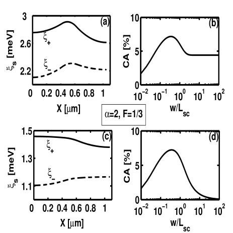
Fig. 2a shows the electrochemical potential profiles in the semiconductor channel for excitation level at which the nonequilibrium density is . This corresponds to light with eV (band gap of GaAs) and power of about 1 W/cm2, when the light is absorbed in a layer of 1 m thickness and all the photoelectrons are then drawn into the 100 nm thick n-type channel. The excitation is restricted only to the sub-gate region so that the inhomogeneous term in the second line of Eq. (10) vanishes. The separation of the ferromagnets is nm which is well within the present planar lithography resolution. The contact widths are nm. Using these parameters we obtain a difference between the left and right ferromagnet currents. We note that the slope of spin-up (spin-down) electrochemical potential is steeper toward the right (left) ferromagnet due to more efficient electrons extraction of this spin. Flipping the helicity results in a mirror image of the spatial profile and in switching roles . The larger current is extracted from the side with the larger spin depletion. Fig. 2b shows the dependence of CA on the ferromagnetic contact width with an optimal value relative to the spin diffusion length. Figs. 2c and 2d show the respective results where the excitation is allowed beneath the contacts and the gate together. The existence of a peak in the CA may be understood by the behavior in two extreme cases. For contacts whose width exceeds the spin diffusion length the behavior is different for both excitation cases. If the excitation is restricted only beneath the gate region than the asymmetry reaches a finite asymptotic value as the spin information is already lost when diffuses beyond this width scale. For non-restricted excitation the fraction which contributes to the asymmetry vanishes if and electrons would tunnel through the barrier under which they were generated. The other extreme of small contacts () results with similar CA dependence on the contact width as most of the electrons are excited beneath the gate. We mention that although the principle of operation of our proposal is straightforward, it is different than the existing electrical measurement scheme with a single ferromagnetic contact on top of the semiconductor layer Hirohata_PRB01 ; Isakovic_JAP02 . If the contacts are separated by less than the spin diffusion length than the spin accumulation profile in the channel ”senses“ the antiparallel contacts. Consequently, the difference in the relative current magnitude from each terminal is sharper compared to the difference in photocurrent from a single contact scheme.
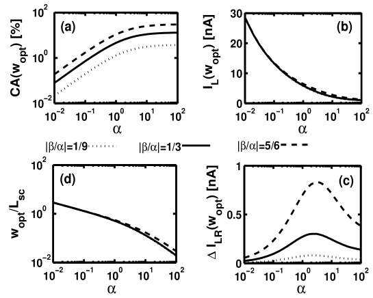
The effect of the barrier’s conductance () on CA may be studied directly by varying the doping profile beneath them. Fig. 3a shows the value of CA for optimal value of the contact width as a function of dimensionless parameter defined in Eq. (8) for three different values of barrier finesse . In all of the following, the excitation is allowed in all regions. The fixed parameters are the spin diffusion length m and the ferromagnets’ separation . Curves for different values of and show that the CA is proportional to and is independent of the excitation level in the linear regime (). The linear dependence on the finesse comes from the difference between two currents being linear in the spin selectivity. We recall that in lateral spin valves electrons traverse two barriers leading to quadratic dependence of magneto-resistive effect on F. In the detector scheme the role of one ferromagnetic contact (injector) is replaced by the photexcitation process (), and when properly designed the carriers may “select” their preferable extracting terminal.
The optimal contact widths for which these CA values were obtained are plotted in Fig. 3d. The lowering of with increasing is understood as follows. For highly conductive contacts, the inhomogeneity of extraction dominates the spatial dependence of spin densities. This means that electrons coming from the gate region will immediately leave the channel when reaching the contact as it would be the path with minimal resistance. Moreover, due to the finite spin dependent conductance and the overall high conductance, photo-excited electrons which are being created beneath the far edge of the contact will rather leave from the same edge leading to further reduction in the asymmetry. This is in contrast to the case of low conductances where the current extraction profile is homogeneous beneath the gates. Finally, we note that is weakly dependent on the finesse of the barriers. This observation simplifies the procedure for choosing the contact width as can be easily obtained from the I-V curve of the junction without need of the knowledge of , which is harder to measure.
Fig. 3b and Fig. 3c show, respectively, the current from the left contact and the magnitude of the current difference between the left and right contacts for excitation with left circular polarization. The semiconductor parameters and the light intensity are the same as before (Fig. 2). The contact length along the z axis of Fig. 1 is 1 m. Although we are using the same excitation level the current is reduced with as the optimal contact width becomes narrower. For the case of =5/6 and the CA exceeds 30%.
V Time dependent analysis
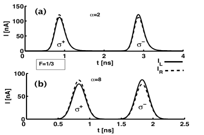
The circular polarization of a pulse of light may also be determined by this spintronics system. We start by a numerical simulation of the time-dependent diffusion equation (3). The initial condition corresponds to a quiescent medium: . Fig. 4 shows the currents through the two ferromagnetic contacts as a result of excitation by two consecutive Guassian-shaped pulses of opposite polarization. The width of the pulses is ps. Figure 4a shows a 0.5 Ghz repetition rate, with all the parameters as in Fig. 2, and using the average light power of 5 Wcm2 (calculated using the same assumptions as in the steady-state case). In Fig. 4b we use barrier conductances four times larger and 1 GHz repetition rate with average light power of 10 Wcm2. In both cases, the peak power is 40 Wcm2. The contact widths have been optimized in both cases according to the steady state analysis above. Accordingly, in the higher conductance barriers case (lower panel) the contact widths are equal to . The contact length along the z axis in Fig. 1 is 1 m. The rise of the current signals follows the light pulses (not shown), although there is ps ( ps) lag between the peak of the light pulse and the peak of the current in Figure 4a(b).
This lag is caused by a finite time which is needed for electrons to leave the channel by tunneling through the barriers.
A simple estimate of a time associated with the flush-out of the photoexcited carrier density is obtained in the following way. Firstly, we set up equations for time-dependence of spin densities after an instantaneous excitation by neglecting the diffusion inside the channel and assuming a spatially uniform distribution. Integrating out the and coordinates in the continuity equation (Eq. (2)) yields,
| (13) |
where and are the averaged current densities at the contact interfaces. In order to express the currents in terms of the non-equilibrium densities, we make use of Eq. (4) and of the relation between the chemical potential and the non-equilibrium density in the linear regime. We arrive at the following equations for the total photoexcited density = and for the photoexcited density polarization :
| (14) |
where the carriers “flush-out” time is given by
| (15) |
The total current out of the system is proportional to , so it decays exponentially with time-constant . This time constant is spin independent and relates only to the total resistances of the FM/semiconductor barriers and of the semiconductor layer ( ). The difference is proportional to the spin accumulation , and decays on a time-scale of . These results agree very well with the numerical calculations using the full time-dependent diffusion equation. We can see that the time-scale after which an excited system returns to its equilibrium state is given by , which limits the repetition rate of light pulses. It is also favorable to have , so that the photoelectrons leave the channel before losing their spin polarization; the time-scale on which the CA effect disappears is bounded from above by the spin relaxation time . However, too short is also undesirable. The explanation of this leads to an alternative understanding of the optimal contact size discussed for the steady state case.
In order to analyze the effect of short , we have to relax the simplifying approximation of uniformity and reintroduce the diffusion processes. A typical time for the density perturbation to propagate through distance is . If the carriers tunnel into each of the contacts faster than they diffuse between them, both contacts do not “sense” each other. The time-integrated CA will vanish in such a case, as electrons leave the channel through the nearer contact, and the average and currents will be the same. The requirement for to be smaller than but larger than leads to inequalities:
| (16) |
where is a typical distance on which an electron has to diffuse to get from under one contact to another. From the above inequalities, we can qualitatively recover the results of Fig. 3a and Fig. 3d. For , spin relaxation is faster than the flush-out time and the right hand side of the inequality is violated. Consequently, further reduction of results in weaker CA effect in agreement with the steady state behavior shown in Fig. 3a. In the limit of large , it is possible to satisfy the left hand side of the inequality by shrinking the contact width compared with the gate width: . The diffusion process is faster than the flushing time if is smaller than . The spin flip processes are of no importance on these time scales as long as so that the right part of the inequality is fulfilled. The CA is maximal in this regime, and , as one can see in Fig. 3d. Satisfying both conditions of the inequality results in high CA effect which in steady state corresponds to the plateau of Fig. 3a. The time domain analysis clarifies the relatively weak dependence on the finesse. This is seen from the flush-out time, the diffusion time, and the spin relaxation time which involve only , , and the length scales of the structure in hand.
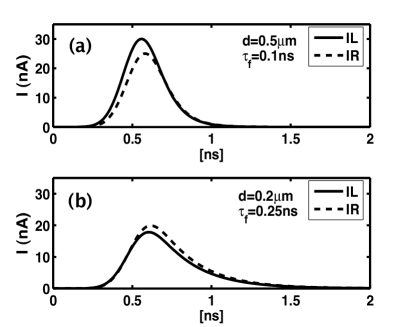
To study the competition between the diffusion and flush-out processes we consider the excitation only under the left contact. The circular polarization of light is such that for uniform excitation in the channel the current from the right contact should be larger. In case (a), we simulate a structure whose total barrier conductance is 1000 cm-2 and whose gate width is 500 nm. In case (b), the respective values are 300 cm-2 and 200 nm. In both cases, the contact widths are 400 nm and the spin relaxation time is 8 ns (possible at lower temperature in GaAs) so that electrons leave the channel without losing their spin information. Other parameters are the same as before. The two cases are presented in Fig. 5a and 5b, where the time-resolved current signal is shown for excitation by a 0.1 ns wide gaussian pulse centered at 0.5 ns. We see that in case (a) the diffusion process is not capable of counteracting the spatial inhomogeneity in excitation and the current from the left terminal is stronger due to the fast flush-out time regardless of the unfavorable polarization. On the other hand, in case (b) the shorter channel and lower barrier conductance enable the diffusion process to fix the spatial inhomogeneity in excitation, and the right terminal manages to extract more carriers as one would expect for homogenous excitation.
In the non-biased system the noise is governed by thermal fluctuations, as the shot noise is irrelevant at predicted current levels. The pulses of 100 ps amount to a bandwidth of 10 GHz so that the Johnson-Nyquist current fluctuations in the highly resistive contacts are of the order of 10 nA. This value is comparable with the difference between and hence sets an lower bound for the pulse widths. In order to improve the performance one should either improve the CA as discussed previously, use stronger excitations in order to improve the signal to noise ratio, or use longer light pulses to decrease the noise bandwidth.
As stated above, in order to increase the repetition rate higher conductance barriers are favorable so that the current transients decay quickly after each pulse. Maximal CA is achieved for comparable resistance of the semiconductor layer and of the contacts but for too conductive barriers the optimal contact width may become impractically small. In the upper panel the time-integrated CA is about whereas the peak to peak ratio is about . In the lower panel both values are around which is probably due to shorter dwelling time in the channel compared with the pulse width (closer to the steady state solution). We have verified that the time independent solution is recovered for pulses whose duration is much longer than .
Ways to increase the current asymmetry
CA may be improved by increasing the spin diffusion length or by increasing the efficiency of the optically excited spin polarization . The latter may be increased from the bulk value by lifting the degeneracy between heavy and light hole bands by strain or by quantum well confinement. Optical_Orientation ; Marie_PRB00 ; Ohno_PRL99 .
Another alternative is to use barriers of higher conductance with smaller contact widths yet still within lithography resolution abilities (e.g. 20 and nm). We note, however, that in the realm of current experiments, Hanbicki_APL03 ; parkin acquiring relatively high selectivity occurs when the ferromagnet/semiconductor interface is abrupt, Jonker_IEEE03 a situation which is achieved with barriers whose parameter is of the order of unity if non-degenerate semiconductor channels are used. This is not the case in MOSFET devices where the source and drain contacts are alloyed into the semiconductor resulting with a low resistivity but at the expense of a rough interface. Sze A possible way to overcome the limitation of low while still acquiring high finesse is to reduce the Schottky barrier thickness. This could be realized by replacing the silicon dopant at the highly doped interface by tellurium, tin or other dopants. Korshunov_compensation For these cases it was measured that self compensation occurred at higher doping levels and that the free carrier concentration was increased by a factor of four. This should halve the thickness of barriers which are presently being used in spin injection experiments, leading to an exponential increase in the contact conductance.
Improvement of the spin selectivity (), as demonstrated by replacing the Schottky barrier with an insulating layer parkin of course helps but it was achieved at the expense of a lower parameter since the conductance of the barrier was very low. This could be improved if a thinner insulator layer is used.
VI Conclusions
We have investigated the time-dependent response of spin diffusion to light stimulation in a realistic lateral structure, which leads to a simple spintronics-based scheme for the electrical measurement of circular light polarization. The simulations were performed using experimentally verified properties of a lateral Fe/GaAs system with thin Schottky barriers. The results imply that spin accumulation in short channels could be tracked in time with relatively high time resolution when the Schottky barriers and the geometry are designed properly. Our analysis provides an aid in choice of system parameters which optimize the detection efficiency. Room temperature detection is possible in short channels or in nanostructures where the current optical detection techniques would be limited by wavelength resolution.
This work is supported by NSF under Grant No. DMR-0325599.
References
- (1) S. A. Wolf, D. D. Awschalom, R. A. Buhrman, J. M. Daughton, S. von Molnar, M. L. Roukes, A. Y. Chtchelkanova, and D. M. Treger, Science 294, 1488 (2001).
- (2) Optical Orientation, edited by F. Meier and B. P. Zakharchenya (Nort-Holland, New York, 1984).
- (3) R. Fiederling, M. Keim, G. Reuscher, W. Ossau, G. Schmidt, A. Waag and L. W. Molenkamp, Nature 402, 787 (1999).
- (4) A. T. Hanbicki, B. T. Jonker, G. Itskos, G. Kioseoglou, and A. Petrou, Appl. Phys. Lett. 80, 1240 (2002).
- (5) S. A. Crooker, M. Furis, X. Lou, C. Adelmann, D. L. Smith, C. J. Palmstr m, P. A. Crowell, Science 309, 2191 (2005).
- (6) R. J. Epstein, I. Malajovich, R. K. Kawakami, Y. Chye, M. Hanson, P. M. Petroff, A. C. Gossard, and D. D. Awschalom, Phys. Rev. B 65, 121202(R) (2002).
- (7) J. Stephens, J. Berezovsky, J. P. McGuire, L. J. Sham, A. C. Gossard, D. D. Awschalom, Phys. Rev. Lett. 93, 097602 (2004).
- (8) K.W. Hipps and G.A. Crosby, J. Phys. Chem 83, 555 (1979).
- (9) M. S. Ünlü and H. P. Zengingönül, Electronics Letters, 32, 591 (1996).
- (10) C. Ciuti, J. P. McGuire and L. J. Sham, Phys. Rev. Lett. 89, 156601 (2002).
- (11) S. J. Steinmuller, C. M. Gürtler, G. Wastlbauer and J.A. C. Bland, Phys. Rev. B 72, 045301 (2005).
- (12) T. Kondo, J. Hayafuji, and H. Munekata, cond-mat0509756, (2005).
- (13) X. Jiang, R. Wang, R. M. Shelby, R. M. Macfarlane, S. R. Bank, J. S. Harris, and S. S. P. Parkin, Phys. Rev. Lett. 94, 056601 (2005).
- (14) F. Garcia, J. Moritz, F. Ernult, S. Auffret, B. Rodmacq, B. Dieny, J. Camarero, Y. Pennec, S. Pizzini, and J. Vogel, IEEE Trans. Magn., 38, 2730 (2002).
- (15) H. Dery, Ł. Cywiński, and L. J. Sham, Phys. Rev. B 73, 041306(R) (2006).
- (16) Z. G. Yu and M. E. Flatt e, Phys. Rev. B 66, 235302 (2002).
- (17) R. A. Smith, Semiconductors (Cambridge University Press, Cambridge, England, 1978).
- (18) A. T. Hanbicki, O. M. J. van t Erve, R. Magno, G. Kioseoglou, C. H. Li, B. T. Jonker, G. Itskos, R. Mallory, M. Yasar, and A. Petrou, Appl. Phys. Lett. 82, 4092 (2003).
- (19) A. Hirohata, Y. B. Xu, C. M. Guertler, J. A. C. Bland, and S. N. Holmes, Phys. Rev. B 63, 104425 (2001).
- (20) A. F. Isakovic A. F. Isakovic, D. M. Carr, J. Strand, B. D. Schultz, C. J. Palmstrøm, and P. A. Crowell, J. Appl. Phys. 91, 7261 (2002).
- (21) X. Marie, T. Amand, J. Barrau, P. Renucci, P. Lejeune, and V. K. Kalevich, Phys. Rev. B 61, 11065 (2000).
- (22) Y. Ohno, R. Terauchi, T. Adachi, F. Matsukura, and H. Ohno, Phys. Rev. Lett. 83, 4196 (1999).
- (23) B. T. Jonker, Proceedings of the IEEE 91, 727 (2003).
- (24) S. M. Sze, Physics of Semiconductor Devices, (John Wiley, New York, 1981).
- (25) F. P. Korshunov, N. F. Kurilovich, T. A. Prokhorenko, and V. K. Shesholko, Inorganic Materials 38, 784, (2002).