Effects of disorder on electron transport
in
arrays of quantum dots
Abstract
Using analytical and numerical methods, we investigate the zero-temperature transport of electrons in a model of quantum dot arrays with a disordered background potential, where the electrons incoherently tunnel between the dots. One effect of the disorder is that conduction through the array is possible only for voltages across the array that exceed a critical voltage . We investigate the behavior of arrays in three voltage regimes: below the critical voltage, above, but arbitrarily close to, the critical voltage, and further above the critical voltage. For voltages less than , we find that the features of the invasion of charge onto the array depend on whether the dots have uniform or varying capacitances. We compute the first conduction path at voltages just above using a transfer-matrix style algorithm. Though only the first path can be studied using this technique, it can be used to elucidate the important energy and length scales. We find that the geometrical structure of the first conducting path is essentially unaffected by the addition of capacitive or tunneling resistance disorder. We also investigate the effects of this added disorder to transport further above the threshold. We find that qualitative behavior is dominated by the presence of the background potential, rather than capacitive or tunneling disorder, at least as long as these additional disorders do not have an extremely broad distribution. We use finite size scaling analysis to explore the nonlinear current-voltage relationship near . The scaling of the current near , , gives similar values for the effective exponent for all varieties of tunneling and capacitive disorder, when the current is computed for voltages within a few percent of threshold. We do note that the value of near the transition is not converged at this distance from threshold and difficulties in obtaining its value in the limit.
I Introduction
It is now possible to engineer arrays of nanoparticles (1-2 nm in diameter) in various geometrical configurations Berven et al. (2002) and to lithographically fabricate arrays of low capacitance islands separated by tunnel junctions with reasonable control over array parameters Kurdak et al. (2000). Such quantum dot arrays (QDA) have been the subject of intense investigation recently Kouwenhoven et al. (1997a, b). In spite of the relatively well controlled properties of these arrays however, there are limitations on the homogeneity of such systems. Disorder at the sub-micron length scales arises due to a variety of reasons, is inevitable and significantly influences the properties of these otherwise well ordered arrays. For ligand coated nanoparticles the variation in coating properties and separation result in different resistances to electron tunneling. As a consequence of the poly-dispersion in the sizes of metallic nanoparticles, the charging energies of the individual islands differ. Similarly for lithographically fabricated tunnel junctions, islands with variable charging energies arise due to a dispersion of island sizes or due to fluctuating capacitative coupling between dots and the underlying gate. Given the pervasiveness of random background charges, nonuniform charging energy and fluctuations in tunneling resistance across the array, an important focus of the current work is to study the effect of these on transport properties of electrons. Due to limitations of the fabrication process, it is difficult to control the different types of disorder independently, whereas this can can be relatively easily addressed by computer simulations.
There are many dynamical systems in which strongly interacting particles exhibit collective transport in a random environment Fisher (1998). Even though the underlying microscopic details are different, systems like the vortex glass in type-II superconductors and charge density waves Fisher (1987), share some general features in the long wavelength limit, e.g., they are both characterized by the presence of a well defined threshold force below which the system is essentially static and above which the system has a non-linear response. Electron transport in disordered QDA also provide a useful system to study problems of qualitative similarity. An advantage of QDA is that the primary interactions and the fundamental physics are relatively better understood and arguably under greater experimental control.
Using a combination of analytic and numerical techniques, we investigate electron transport at zero temperature in arrays of disordered small capacitance islands which are capacitatively uncoupled to their neighbors. We use this system both as a model for collective transport of discrete charges in a random environment and for better understanding the role of disorder. By studying similar systems, but for different values of parameters, different regimes of the collective transport problem can be addressed. These regimes may be characterized by the relative strengths of disorder, tunneling rates and electron-electron interaction. These regimes are accessible experimentally too, as arrays can be fabricated with varying degree of tunability of the coupling between the array elements Duruoz et al. (1995). For example, the model in Refs. [Enomoto, 1999, Granato and Kosterlitz, 1999] is similar to the model we study in this paper – in that offset charge disorder is included, although Gaussian distributed as opposed to uniformly distributed – but the screening length is assumed infinite. (Transport in this regime is believed to belong to the same universality class of two dimensional magnetic vortex model in disordered superconducting films.) Ref. [Hirasawa et al., 1998] which investigates 2DEG at semiconductor heterointerfaces designed to keep the self-capacitance and disorder low – the I-V characteristic is better explained by charge soliton injection as no threshold voltage is observed. Such systems can be used to study two dimensional Coulomb gases which undergo charge Kosterlitz-Thouless (KT) transitions.
I.1 Outline
There have been many experimental and simulation papers Parthasarathy et al. (2001); Parthasarthy et al. (2004); Kurdak et al. (1998); Rimberg et al. (1995); Ancona et al. (2001) (to cite just a few) which have used the theory developed in Ref. [Middleton and Wingreen, 1993] by Middleton and Wingreen (MW). This paper expands on the MW discussion of electron transport in disordered arrays. The original model and its extension to include other forms of disorder are described in the remainder of this section. One-dimensional arrays – both below and above threshold – are discussed in detail in section II. In section III results for 2D arrays below the threshold voltage are presented including several results not discussed previously. As the original MW paper sketched only briefly the connection between the independent conducting paths and the properties of a directed polymer in random media (DPRM), a major aim of section IV and III is to establish the connection on a more rigorous basis. In section IV we discuss the morphology and current carrying properties of the first conducting path at threshold for QDA. It also provides some of the details required to understand the non-linear scaling of current (I) with voltage (V), which is addressed in section V.
There have been several papers that have used numerical approaches to investigate transport in arrays (both 1D and 2D) in the presence of random background charges as well as other types of disorder Kaplan et al. (2003); Melsen et al. (1997); Johansson and Haviland (2001); Ancona et al. (2001). Some approaches, have used discrete event simulation techniques to model the individual tunneling events, whereas some have explicitly used computed transition rates in a master-equation approach. The common aim is to compute the general I-V characteristics, which as a consequence of the collective behavior of electron tunneling is non-trivially dependent on the individual rates. We focus on a statistical physics approach to the problem, thus laying a theoretical basis for the scaling exponents observed experimentally and numerically.
I.2 The Model
The three main energy scales of QD are the charging energy (), the electron in-a-box energy levels () and the thermal energy (). As a consequence of the small size of these islands and tunnel junctions the capacitance involved are in the femto to atto-Farad range, thus the charging energy – which is the increase in energy due to the addition of a single electron is given by – of these islands is large. A characteristic feature of QD is the clear separation of internal energy scales and . An external energy scale () is set by the temperature of interest, which determines the levels that are resolved and participate in transport. When the role of thermal fluctuations can be ignored. Depending upon the temperatures of interest, maybe comparable to or different; for , the discrete energy level spectrum of the QD do not play a role during transport. Metallic dots are different from semi-conducting dots by the fact that typically the level spacings for metallic dots are much smaller compared to other energies. At sufficiently low temperatures, the scale of which is set by, , the addition of a single extra electron to an dot increases the dot energy; in spite of the increased energy, the dot is stable to thermal energy fluctuations, which in turn makes it unfavorable for more electrons to tunnel onto the same dot, resulting in its blocking other electrons onto the dot. This is called the Coulomb blockade regime.
The parameters required to characterize QDA can vary over a large range of values and consequently so do the properties of QDA. Thus, it is instructive to understand the parameter space of QDA in order to appreciate the details of the model. The main parameters used to characterize QDA, as opposed to individual quantum dots (QD) are: the tunneling resistance () which to a first approximation is a measure of how well confined the electrons are on a dot, the inter-dot capacitance () and the dot capacitance () which is a function of the junction, gate and self-capacitances. The relative values of and are important as it determines the extent of electrostatic coupling between dots in the array. The exact value of depends on the system under consideration. For example, typically the self-capacitance of lithographically prepared arrays is negligible compared to the other capacitances, thus is a function of the dot-gate and tunnel junction capacitances (for example in Ref. [Kurdak et al., 1998] = Cg + 4C). For nanoparticles with diameters of a few nm, the self-capacitance becomes important and should possibly be considered in the computation of Berven and Wybourne (2001). Either way, still sets the scale for the charging energy. Independent of the actual experimental setup considered, as long as , the dots are considered to be capacitatively uncoupled to each other and the electrostatic energy is determined by on site interactions only. However if is comparable or less than the dots are capacitatively coupled. A screening length () can be thought of the distance (in units of dots) upto which the charge on a dot can be felt electrostatically, i.e., distance that an excess charge placed on a dot will effect neighboring dots by polarization. The polarization decreases exponentially with , which in turn decreases with the ratio of ; this is consistent with understanding that there is a stronger screening of the electrons on a dot from electrons on adjacent dots as the capacitative coupling between a dot and the back gate increases. For , .
The main modification to the original MW model is the introduction of nonuniform dot capacitance and tunneling resistances . The effects of underlying charge impurities trapped at the interfaces and in the substrate are captured in a random background charge on each dot. The effect of background charges is modeled as offset charges on each dot (). The offset charge at any site is considered to be [0,1[, as any value outside this range will be compensated by electron hopping. Arrays with only offset charge disorder are referred to as UC (uniform capacitance) systems. The area and capacitative coupling of an island to the underlying electron gas varies from dot-to-dot in an array. These fluctuations in the dot-gate and self-capacitance of dots, along with stray capacitances are incorporated by assuming a varying dot capacitance . As controls the charging energy of the dot, a non-uniform results in different charging energies of dots. Arrays with both offset charge disorder and a varying , are referred to as DC (disordered capacitance) systems. Fluctuations in the tunneling resistance – either due to varying distance between metallic dots or the varying material properties of the tunnel junction separating the metallic islands between dots – is captured by assuming a log-normal distribution of tunneling resistances. Arrays that incorporate variation in tunneling resistance as well as offset charge disorder, but with a fixed value of , are referred to as RT (resistance disorder) systems.
We assume small metallic islands are separated from each other by tunnel junctions of resistance but capacitatively coupled to neighboring dots (). We assume a constant capacitance between neighboring dots and between the left and right leads and dots adjacent to them. The dots are assumed to be separated from an underlying back gate by an insulating layer. Each dot is capacitatively coupled to the back gate with a capacitance . The leads and back gate are assumed to have infinite self capacitance. As a consequence of the proximity of the back gate to the dots , the screening-length is taken to be less than one lattice spacing. Consequently the capacitative coupling between dots is neglected.
We will consider arrays where the single-energy levels of the dots are essentially a continuum at the Fermi level in the strongly Coulomb blockaded () regime. Thus tunneling is between levels determined by . Where a spread in values of is considered, we assume tunneling resistance between any two dots is still sufficiently large to consider electrons localized on a site (). This is the regime of the “orthodox theory” of single electron tunneling and is applicable for both the micron sized lithographically defined SET (e.g., metal islands embedded in a substrate Rimberg et al. (1995) and separated by tunnel junctions or semi-conductor islands separated by barriers Duruoz et al. (1995)) as well as the 3D metallic grains. According to the “orthodox theory” Averin and Likharev (1991) of a tunneling event across a tunnel junction, tunneling rates (transition probability per unit time) associated with an event are given by,
| (1) |
where is the difference in the free energy of the system before and after the tunneling event, is the tunneling resistance of the junction involved in the tunneling event, T the temperature and is the usual Boltzmann constant. The kinetic energy gained by the tunneling electron is assumed to be dissipated. The value of is assumed to be much greater than . This essentially implies that the wavefunction of electrons are localized to a single dot which permits the number of electrons on any single dot to be treated as a classical variable. It should be pointed out that the orthodox theory is still valid for arrays in the limit , but not for dots in the other limits of and .
In this limit the energy is all electrostatic and is determined by a capacitance matrix and is represented as:
| (2) |
where () are the charges on the left (right) leads, which are at voltages () and is the inverse of the matrix of capacitances between dots and . The diagonal elements of are the sum of all capacitances associated with a dot and the off-diagonal elements are the negative of the inter dot capacitances. Hence for a NN array in the limit of 0, the capacitance matrix is a NN diagonal matrix.
In the limit of small screening length (less than 1 dot spacing) and the presence of offset charge disorder the voltage on dot i is given by is .
At zero temperatures the expression (1) for tunneling rates reduces to
| (3) |
hence a charge may tunnel from dot i to j, only if such an event lowers the free energy of the array i.e.
| (4) |
II 1D arrays
Before attempting to understand the detailed properties of two dimensional arrays, we begin by an attempt to understand the relatively simpler case of a linear chain of quantum dots, as they facilitate an understanding of some of the ideas required later. There have been several experiments aimed at understanding the conduction properties of essentially one dimensional arrays of nanoparticles Bezryadin et al. (1999); Berven and Wybourne (2001). The ability of metallic nanoparticles to be patterned using polymers templates makes them attractive candidates for potential future self-assembling electronic devices.
II.1 Uniform : Insulating State
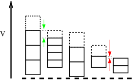
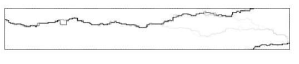
We start by exploring the tunneling of electrons onto the array from the emitter lead. In the zero temperature limit, as the capacitance of the leads is assumed to be infinite, electrons can flow onto the array when the voltage of the emitter lead () is equal to or greater than the voltage of the leftmost dot as given by Eqn. 4. At this applied voltage, an electron cannot tunnel from the leftmost dot to the next dot, say represented by the index , if dot has an offset charge impurity greater than the offset charge impurity of the leftmost dot. Electrons tunnel onto the array only if it is possible to do so without an increase in the free energy of the system. This is no longer possible for the configuration in Fig. 1. In this configuration the electron residing on the leftmost dot is considered to be pinned.


As shown in Figs. 1 and 1 the emitter lead voltage has to be increased by at least one unit in order that the electrons can overcome the barrier. As the value of the emitter lead voltage is successively increased, there will be a cascade of electrons tunneling onto the array from the lead, until they get progressively pinned and it is no longer energetically possible for electrons to penetrate further into the array. The flow of charges onto the array at a given emitter lead voltage until they are all pinned due to the disorder and thus no further electrons can tunnel onto the array constitutes an avalanche.


There exists a unique value of the emitter lead voltage – which depends upon the underlying disorder profile – at which electrons will be able to reach the collector lead for the first time (Fig. 1). This well-defined voltage value is referred to as the threshold voltage (). separates the conducting phase from an insulating phase. Typically in order to reach the collector lead end of an array L dots long, an electron will have to overcome upward steps. These steps can be can be understood as the average number of steps a random walk in 1D makes in a given direction, thus the mean threshold voltage should be given by
| (5) |
where the over-bar represents an averaging over disorder realizations. Sample-to-sample fluctuations in the can be thought of as the root-mean-square fluctuations of a random walk in 1D which scales as , where N is the number of steps of the random walk. Hence fluctuations in should scale with system size as
| (6) |
The scaling of both and with system size, as shown in Fig. 2 are consistent with the above explanation.
II.2 Uniform : Conducting State
The threshold voltage represents the lowest voltage at which electrons can tunnel across the array, hence for , current flows through the array. For a given disorder realization, depends on the number of up-steps encountered due to the offset charge impurities.
If is marginally greater than , so that , then the discreteness of charge and offset charge impurities play a crucial role in determining the current. At these voltages the current is determined by the slowest tunneling rate () between any two neighboring dots in the array (analogous to the net flow of traffic being determined by the bottleneck in the path of flow), which on the average is given by , where L is the number of dots in the 1D array.
This can be understood as follows: represents the voltage increment over . In principle the voltage drop can be anywhere between between 0 and for a given pair of dots. For an array with L dots there are L+1 ( L when L is large) voltage drops (tunneling rates), hence the minimum voltage drop across any two dots is on the average , which results in a tunneling rate given by Eqn. (3) to be . Using we get = . As we have
| (7) |
As can be seen from simulation results in Fig. 3, in the limit of low and for large system sizes, the local value of the exponent is consistent with 1. Note that the for smaller system sizes (L 1000) the effective exponent is quite far away from 1. The fact that chains at least larger than 1000 are required is an important observation. We will revisit its implication later in the chapter.
In the opposite regime of a high applied voltage, , the current is determined by the average tunneling rate across a pair of dots. This is given by the of the average voltage drop across a pair of dots, , i.e., , which gives the same scaling expression for the current with as Eqn. (7). For values of , a crossover from slow point dominated current linear scaling to high applied voltage linear scaling is observed.


II.3 Non-Uniform : Insulating State

As mentioned, the introduction of dots with non-uniform leads to an array with dots of different charging voltages. For our simulations, we assume to be uniformly distributed between 1.0 and a maximum fluctuation of 2.0. If we attribute the variation in by a factor of 2 to fluctuations in the size of the dots, it corresponds to a change in a variation in the linear dimension of dots by a factor of . The determination of the gets complicated by the presence of both offset charge disorder and varying charging energies. This is illustrated in Fig. 4 where the spacings between voltages are different for different dots; this is in contrast to dots with uniform as shown in Fig. 4. The increment in voltage required in order to tunnel between a pair of dots is due to two independent random variables – and , where is the charging energy of dot i and is between 0 and 1 which represents the required increment due to the offset charges. can be written as the , where the summation runs over the number of dots in the array, L. can therefore be written as , where represents the average values. Hence
| (8) |
where is for the assumed maximum value of 2.0. Although scales as L, similar to the UC arrays, behavior is more complicated. An exact analytical expression for – which can be derived using the expectation values of and gives,
| (9) |
Thus, up to leading order scales as . This is consistent with our results as can be seen in Fig. 2.
An often used technique to explore the disorder energy scale is to study the response of the system on changing the boundary condition Bray and Moore (1987). For disordered 1D QDA, we change the boundary condition at the right lead and study the change in threshold voltage. We define as the difference in on changing the value of by . Recall that for UC arrays was completely determinable by the number of up-steps in the offset charge impurities. For the uniform capacitance case the response is trivial: a shift in the by – where is or a multiple thereof – changes by the same amount. This is a consequence of the response being periodic in voltage. For the 1D QDA with disordered capacitances, however, a shift in by guarantees a change in by only on the average, due to a consequence of the threshold voltage being invariant to the zero-level of the lead voltages. Specific values of depend upon the specific disorder configuration. As a consequence of the invariance just mentioned,
| (10) |
where ( ) is the probability that the threshold voltage changes (does not change), the average of the non-zero values of . Also is 0.


The response to a change in the right lead voltage can be formulated in terms of a 1D random walk problem. Given the initial and final points of a random walk, one can ask what is the probability that a random walk starting a distance a from the initial point of the original walk, intercepts the original walk before a distance ? If we assume that interception with the original walk results in annihilation, we can ask of the surviving walks – what is the typical separation of the end-point of surviving walks from the end-point of the original random walk? It is known Fisher (1984), that the probability of “survival” decreases as and the typical separation scales as (the square root of the mean standard deviation of a step random walk). The mapping to the random walk problem is carried out by considering as the origin of the walk, the potential of each dot at threshold (minus the gradient) to be the positions of the original random walk and finally as the distance of the initial point of the second random walk from the original random walk. Thus, we expect that the probability of (i.e., survival) and the mean of the non-zero () should scale as L and Lrespectively. This is consistent with our numerical results as shown in Fig. 5 , although there are significant deviations at smaller system sizes.
II.4 Non-uniform : Conducting State
We discussed earlier how for UC arrays in the regime of low , the value of the current is determined by the presence of dynamically important slow points. An important distinction that arises in DC arrays is that the location and value of slow points is less regular. For UC arrays, the value of smallest voltage drop – and hence the minimal tunneling rate – was bound to increase every time the emitter lead voltage was incremented by one unit ().

Unlike UC arrays, the amount by which the emitter lead voltage must be increased in order to overcome the slow point does not have a well-defined lower bound and varies significantly from sample-to-sample and with the value of reduced voltage. As can be seen from the presence of plateaus in Fig. 6, the I-V at low for a single DC array is qualitatively different to a sample-averaged I-V.
At a given value of , the mean tunneling rate () is proportional to the average potential gradient, and is given by,
| (11) |
Based upon the relative values of the and the typical maximum fluctuations from , we can categorize the applied voltage into three regimes. These regimes are: (i) when the maximum fluctuation are larger then the mean tunneling rate; (ii) when the maximum fluctuations are of the same value as the average gradient, and (iii) when the maximum fluctuations are much less then the average gradient.
In regime (iii) the fluctuations about the mean gradient can be ignored; they no longer influence the current value and consequently the current is given by the Eqn. (7). The average potential profile at any given dot can be computed using the average potential gradient and the distance of the dot from the boundary. By subtracting the dot potentials from the averaged potential profile at each site, we can calculate the fluctuations, and thus the roughness of the voltage surface. In regime (i) the roughness of the voltage surface scales as L. Assuming Gaussian distribution of the fluctuations, the mean value of the maximum of N variables from a distribution with mean and standard deviation is given by + Kinnison (TBD). The deviation from the mean tunneling rate is maximum at the slow point. Given that the slow point can occur anywhere between any two dots (i.e., 0 and L), the typical value of the maximum fluctuation scales as + . The increment in voltage should thus be greater than the maximum barrier (fluctuation) in order that the slow point be overcome, i.e., an additional electron flows over the slow point which in turn will result in an increase in current. Therefore the probability that a change by will overcome a slow point is given by the probability that the typical maximum fluctuation is less than . As , P( typical maximum) , which approaches 1 as L gets larger.
If step like features persist in the I-V for single samples, then given the sample-to-sample fluctuations in the location of the plateaus, the sample averaged I-V curve will be more or less flat. As seen in Fig. 7, there is a voltage upto which the averaged current is more or less static. The value of this voltage decreases with increasing system size – consistent with the arguments that the same increase in is more likely to result in a slow point being overcome as L gets larger. In spite of the irregular change in the value of the minimum rate, the average value of the minimum voltage drop across any two dots remains . Hence the average value of the minimum rate remains as before – , which implies that once the “static current regime” is overcome the current should scale linearly with voltage. Thus in spite of the introduction of variable , current scales linearly with in regimes (i) and (iii), similar to UC arrays. The crossover from linear scaling in regime (i) to (iii) – corresponds to regime (ii) and is more complicated to understand analytically.


In Fig. 7 and Fig. 7 we plot the current and local exponent values for the largest systems (L 500). As shown in the plot of effective exponents (Fig. 7), numerically we find = 0.85 0.02 in the low voltage regime (0.05 0.5) and 1.2 in the high voltage regime ( 1.0). Similar exponent values are found for system sizes less than L=500 (not shown).
III 2D Arrays: Insulating State
We saw in the previous section, how for one-dimensional arrays, charge flowed onto the array from the emitter lead till it was energetically favorable. In this section we will attempt to develop an understanding of the progressive build up of charge in two-dimensional arrays, as the emitter lead voltage () is increased; the tunneling of charge is still governed by Eqn. 4. The flow of charge onto the array can thus be viewed as lowering the energy. Such relaxation of charges so as to lower the system energy, is analogous to several different systems where the system reaches a lower energy via a series of avalanches Fisher (1998); Watson and Fisher (1996).
The threshold voltage is the minimal emitter lead voltage possible such that when electrons tunneling onto the array from the emitter lead have sufficient potential to overcome the disorder barriers and reach the collector lead. Given a disorder configuration it is not trivial to determine the minimal voltage for 2D arrays. A naive approach might be to think of the LW array as W, 1D arrays of L dots each; trivially compute the “threshold” voltage for each of the 1D arrays and then find the minimum. The computed minimum would still probably be overestimating the true threshold voltage. Determining the threshold voltage can be formulated as an optimization problem, but motivated by the aim of understanding the physical buildup of charge in QDA, we take a different approach. For a given emitter voltage, we add charges till a meta-stable insulating state is reached; then the emitter lead voltage is progressively increased, building up charges until an insulating state no longer exists. The value of the emitter lead voltage at which electrons first tunnel onto the collector lead is our computed threshold voltage.
III.1 Avalanches
As briefly mentioned earlier that an avalanche at a given voltage is the flow of charge onto the array until the flow is arrested by disorder. Avalanches in QDA are qualitatively similar to those found in other systems with collective elastic transport. Some well studied examples are vortex flow in disordered superconductors Bassler et al. (2000) and the avalanches when an interface like a CDW moves in quenched disordered systems Narayan and Middleton (1994); Middleton and Fisher (1993). For 2D arrays, the location where charges tunnel in a given avalanche, helps develop the notion of connected elastic domains – basins.
We define as the charge of site before the emitter lead voltage is incremented to and as the charge of site after the emitter lead voltage has been incremented to . The physical size of an avalanche is the number of sites where , and the volume is . If we set to be the number of avalanches between size and , at an emitter lead voltage of and define = , then can be thought of as the number of such avalanches that occur in going from a = 0 to = .


We explore the distribution of avalanche sizes for square samples (LL). The size of an avalanche can also be thought of as the “surface area” – which is equal to the number of dots that electrons tunnel onto during an avalanche at a given . As the size of avalanches vary over several orders of magnitude – starting with avalanches of size 1 to system spanning avalanches – we use logarithmic bin sizes. Logarithmic binning is natural for exploring power laws and reduces fluctuations in plots.


Using standard finite size scaling, we conjecture a scaling form for to be of the type:
| (12) |
where scales as in the limit of and approaches a constant in the limit of , where is the length of the system. The exponents and are determined to be those exponents for which a scaling plot of vs yields a single scaling function . The two exponents are not independent and can be shown to be related by the relation . 111The sum of the product , for all avalanches upto threshold, scales as (for systems of size LL), from which the relation can be derived by using the scaling ansatz in the integral, . For logarithmic binning as , where n(A) represents the number of avalanches in the linear bin []. In addition to the two exponents and , a third exponent , can be used to make the curve flat in the regime where , which for square systems of length and width L is related to the other two exponents by . 222for avalanches of size , N(A) scales as . Also for , where c is 0, which for a given A leads to , i.e., . As there are two constraints for the three scaling exponents, we get only one independent exponent from the scaling collapse of the distribution of the sizes of avalanches. As shown in Fig. 8 the collapse of data to a single scaling function is satisfactory, which indicates that the dimension of the avalanches is . The typical size of the largest avalanches is given by L. To study further the morphology of the avalanches, we compute the the mean of the maximum length of avalanches with sizes between A and A+dA. We collapse the data as shown in Fig. 8 onto a single curve and determine that exponents and , defined in the scaling function:
| (13) |
to have values consistent with and 1 respectively. We get a collapse to for all system sizes L, thus and the relation constraining the exponents is therefore or . We know that the , where is defined to be the fractal dimension, from which we get thus . From the computed values of and , works out to be 1.5. This is consistent with the conclusions from the distribution of avalanche sizes.
Finally, we have also investigated the avalanche structure using the radius of gyration () of avalanches, which is defined in the usual way as:
| (14) |
and study the scaling of the mean for avalanches of sizes between and . Numerical evidence Jha (2004) indicates that the scaling of the area with is similar to the fractal dimension of the avalanches, which implies that the avalanche morphology is compact, i.e., does not have any significant holes.
We have investigated avalanche structure using three ways and the results of all three are consistent with the hypothesis that typical avalanches are compact with dimension of . For systems with uniform , the sequence of dots at which avalanches originate is periodic in left lead voltage (with periodicity ). We can thus think of “basins” of dimension evolving as charge flows into the array, with some basins growing at the expense of others. In general the basin structure is not isotropic, as they have a preferred growth direction and the linear size in the direction transverse to this preferred direction grows only as where l is the linear extent in the preferred direction. Thus in a square samples of length and width L, there are approximately independent regions of activity, where is defined as the number of basins at a distance from the left lead. Hence to increase the chances of having the large basins that scale with L, we simulated systems of length L and width a multiple of L (width = Nb L).


Similar to square samples, exponents in the scaling collapse for the distribution of avalanche sizes for systems of size LL (Fig. 10), are not independent but constrained by two relations.
Given that the total number of dots is L the sum of the product scales as L rather than L3.0; hence . Also the number of avalanches in the bin [A, A+dA] scales as L , so in this case.
An important difference in the avalanche structures between the uniform and disordered systems is the lack of periodicity (irregular) in emitter lead voltage and that the basins no longer evolve by quenching other basins (they overlap).
Avalanches in DC arrays are not periodic in emitter lead voltage and basins don’t typically evolve by quenching other basins – they tend to overlap. This behavior is different to UC arrays. By using the three methods discussed earlier we find that capacitance disorder does not affect the structure of the avalanches. Fig. 9 shows the scaling collapse for the distribution of avalanche sizes N(A), for square arrays with nonuniform . The constraining equations in this case are now (as the sum of the product of N(A)A for all avalanches ) and . In spite of the presence of capacitance disorder, the value for the exponent is the same to within errors for the value for uniform . Exponents characterizing the scaling of mean linear size and mean with area for DC arrays also agree to within errors with exponent values from UC arrays. Thus avalanches remain essentially compact with a dimensionality of . For LL DC arrays there is no change in the values of the exponent a, though the constraining equations change to and Jha (2004).
In this subsection, we have used finite-size analysis and been able to successfully relate several finite-size exponents via scaling relations. Table 1 provides a quick summary of the values and the context in which they are used. Taken along with the fact that these exponents and scaling relations help characterize the transition from an insulating to a conducting state (the conducting state is yet to be discussed), it is reasonable to view the transition as a critical transition with associated critical exponents and behavior.
III.2 Interface motion
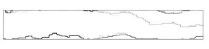
The maximum advance of charge into the system at a given can be used to define an interface. Properties of the interface can be used to understand other properties of the system like fluctuations in . Some details are required about the way we define the interface. At a given , there will be some dots onto which electrons have not tunneled yet, defined relative to the original stable configuration reached by relaxing an original configuration with . We refer to such dots as zero excess dots. We can define the interface as either of the following: (i) contour of leftmost sites along each row which has not had an electron tunnel onto it, or (ii) the contour of last sites along each row which has had an electron tunnel onto it. The two although seemingly similar are different in the sense that the second definition considers the case where there may be “bubbles” of zero electron dots enclosed behind the interface. The difference, however, is not significant as the long wavelength properties of the interface (e.g., roughness) do not seem to depend upon which definition is used. As is increased, electrons tunnel onto arrays, via avalanches and if electrons tunnel onto a zero excess dots, the interface advances. The motion of the interface in response to a driving force, can be described in the language of an elastic medium driven through a random potential. We will argue that some quantitative correspondences exist in fact. The dynamics of such elastic interfaces through quenched disorder has been extensively studied in recent years Barabasi and Stanley (1995), e.g., CDW, flux lines in type II superconductors etc, fluid flow through a porous medium to name some, flux front in thin films of type II superconductors Surdeanu (1999), combustion of paper Maunuksela (1997); Alava and et al (2000).


We define the roughness (width) of the interface as the square root of the mean of the square of the fluctuation from the mean position. On increasing the interface advances further into the system and gets rougher. As charge builds up behind the interface, the advance of the interface is analogous to the growth of a surface due to deposition of a material. It is well known, that such surfaces become increasingly rough with time, gradually reaching a saturation width. For QDA as the advance of the interface is governed by ; it plays the role of time, which upto a constant factor is the same as the mean position of the interface. Using the well known scaling form Family and Vicsek (1985):
| (15) |
we were able to collapse data on the width of the interface with time onto a single scaling curve Fig. 11. We initially used symmetrical LL systems to study the properties of the interface. Due to the large values of the dynamic exponent z (1.5), we were able to study only small system sizes with interfaces with saturated width. Consequently in order to study steady state properties of larger interface lengths, it is prudent to study non-square systems like LL, thereby permitting a more accurate determination of the exponents and hence the universality class the interface growth process belongs to.
From the the collapse in Fig. 11, we find values of the roughness exponent = 0.5 and dynamic exponent z = 1.5 – therefore the growth exponent = 0.33. This is consistent with the roughening of the interface being in the KPZ universality class Barabasi and Stanley (1995), where = and = . The KPZ universality class is consistent with the symmetries of the system, viz., rotation is a symmetry on large scales Middleton and Wingreen (1993), interactions are short range and the speed of the interface advance lacks large fluctuations. In light of the assumed lack of spatial correlation of the underlying charge disorder for dot arrays (statistically Galilean invariant) and the fact that the interface will move forward when the emitter lead voltage is increased by one unit (), a description of the interface advance in terms of thermal KPZ equation seems valid.
Some avalanches involve electrons hoping onto a zero excess dot – a new-site. When an avalanche involves new-sites, the interface is reconfigured; the distribution of the avalanches that involve new-sites provides information on the reconfiguration (advance) of the interface.

The scaling collapse for the distribution of avalanches that have between s and s+ds new-sites for UC arrays is shown in Fig. (12). We define analogous to , where is the number of new-sites visited in an avalanche. For LL samples the sum of the product for all avalanches, scales as the number of dots in the array (L ). Thus the constraint on the exponents and in the scaling ansatz:
| (16) |
is given by . Another constraint is determined by the scaling of the number distribution of avalanches with the number of new-sites for a given bin ([s, s+ds]), with system length as L , which results in only one independent exponent in the scaling ansatz. Hence . We find that the exponent values from the collapse consistent with these constraints. We interpret the value of the exponent = 0.67 as giving the typical number of new sites involved in an avalanche of linear length l as l0.67. We know that the width of the an avalanche of linear length l, is also l, which indicates that the avalanche typically involves one new dot for each dot along the width. Thus the interface advances smoothly on the average by 1 dot along the width of the basin of activity. Fig. 12 shows the configuration of the interface at a given and an avalanche that crosses the interface with the portion to the right of the interface being the new-sites involved in the avalanche. These new-sites will determine the new configuration of the interface after the avalanche.

Further information on the movement of the interface can be obtained by studying the voltages (VL) at which an avalanche that involves new-sites occurs, or equivalently when the interface advances. We can define as the difference in between two avalanches that manage to cross the interface (there may be several avalanches that do not cross the interface between two interface crossing avalanches). Based upon the assumption that the advance within basins should be independent, it can be shown Jha (2004) that scales as Wl.
We’ve seen how the structure of the avalanches is the same irrespective of the presence or absence of disorder in the capacitance, even though there are changes of major significance in the motion of the interface. If however, as shown in Fig. 13 we attempt a scaling collapse for the number of new sites covered in an avalanche the exponent values are different from the uniform exponent values. The exponent has a value 1.0 to within errors. This value can be interpreted as follows: the dimensionality of avalanches is , which means for linear size the width is typically . When an interface crossing avalanche occurs, the average amount by which it overshoots the interface scales as , hence covering x new sites.
This can be seen in Fig. 13, which represents a typical interface crossing avalanche in a sample with disordered , where the avalanche overshoots the interface by a significant amount compared to the uniform (where the overshoot was of order one spacing). For DC arrays avalanches do not occur with any fixed regularity – either spatial or temporal – so a large number of avalanches may occur which do not reconfigure the interface, followed by an avalanche that rearranges the interface by a large amount. Compared to the smooth motion of the interface in arrays with uniform , the motion of the interface for DC arrays is rather jerky. It is important to mention that the motion appears jerky locally, but at a coarse-grained scale and on average the velocity of the interface is well defined and smooth till it reaches the collector lead.
III.3 Threshold voltages revisited
Similar to one-dimensional systems the for two-dimensional systems scales linearly with the system length. For two-dimensions however, there is an additional dependence on the width of the samples, which can be understood using the concepts of basins and interface advance from earlier subsections. It also helps explain voltage fluctuations.


With increasing the interface advances further along into the system until finally electrons reach the collector lead at . Fig. 14 shows how normalized by system length (L) depends upon the width of the system studied. When 1, in addition to fluctuations within a single basin, is determined by the basin that moves the interface to the right lead the earliest. With increasing , the expectation value of the maximum advance of the interface at a given increases, explaining the decreasing value of . The sample-to-sample fluctuations in can be attributed to the roughness of the advancing interface. We saw that the roughness exponent for the interface was . Assuming a value of z= , for L W samples, where W = L the interface reaches its saturation width given by W, which is L . As shown in Table 2, fluctuations in agree with this picture. Local values of the threshold fluctuation exponents are plotted in Fig. 15 and 15 and they are consistent with the scenario depicted.


A finite-size scaling length can be defined in terms of the characteristic fluctuations in . can be thought of as defining the scale characterized by , where is the exponent characterizing the finite-size effects on the transition and for both uniform and disordered systems has a value of .
Analogous to the 1D systems, we investigated the response to changed boundary conditions – measured by the change in right lead voltage – by measuring difference in , as a method of probing the disorder energy scale. It is shown Jha (2004) that scales as L, i.e., for 2D when changes, it changes on average by a value given by L. We have discussed the mapping between Eden growth (which is in the KPZ universality class) and DPRM Roux et al. (1991). Using the analogy, the maximum point of advance of the interface in our systems can be mapped to the ground state of a DPRM. It is known that the free energy fluctuations of the ground states, both for sample-to-sample fluctuations and higher order excitations scale as L. For systems whose ground state (maximum advance of interface) is unable to overcome the increased voltage of the right lead (a change in boundary conditions) the next lowest energy state (interface position) needs to be enough to overcome the changed boundary condition; the energy of which is typically L higher than the ground state. The L behavior can be understood without invoking the mapping between Eden growth and DPRM. We saw in the subsection on interfaces, that the mean voltage increment to move the interface so as to have a new maximum position scaled as L . When the right boundary condition is changed, either the last avalanche is able to overcome the increased right lead voltage (in which case ) or requires an increase in , in order to surmount the barrier at the right lead.
| Symbol | Used in | uniform | non-uniform |
|---|---|---|---|
| a, b, c | N(A) vs A | 1.7, 1.3, -0.43 | 1.7, 1.1, -0.55 |
| , , | l vs A | 1.0, 0.63, 0.58 | 1.0, 0.67, 0.67 |
| , , z | Family-Vicsek scaling | 0.5, 0.33, 1.5 | 0.5, 0.33, 1.5 |
| , , | N(s) vs s | 0.67, 1.0, -0.3 | 1.0, 0.67, -0.05 |
| fluctuations in | 0.33 | 0.33 | |
| mean of nonzero | 0.0 | 0.3 |
| uniform | non-uniform | |
|---|---|---|
| 1 | 0.33 0.01 | 0.33 0.01 |
| 2 | 0.34 0.01 | 0.34 0.01 |
| 4 | 0.35 0.01 | 0.34 0.01 |
| 8 | 0.36 0.02 | 0.35 0.01 |
In addition to a well defined critical point, a true continuous phase transition is characterized by the fact that there aren’t any characteristic length scales in the system, i.e., fluctuations take place at all length scales. Obviously this is not true for finite size systems – where possibly all length scales upto the system size, but no larger can be present. This system-size dependent cut-off explains why we see finite-size deviation from the true (infinite-size) values. There is a systematic dependence of these deviations with the system sizes studied. By examining these systematic dependences on the scaling exponents, we try to extrapolate to the infinite-size value of the exponents. The fact that a system-size independent behavior is possible over a range of system sizes (e.g., the collapse of several system sizes onto a single curve) is the crucial indication that finite-size scaling approach is successful, which in turn is an indication of a phase transition. Hence the claim that can be viewed as the critical point of a phase transition.
IV 2D Arrays at Threshold
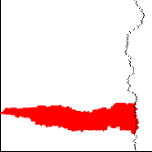
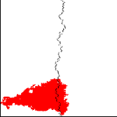
is defined as the lowest lead voltage at which there exists at least one dot in the column adjacent to the emitter lead, onto which electrons can tunnel and subsequently find a way onto the collector lead. Having established the existence of a threshold voltage in the previous section, our aim in this section is to understand the current conduction in the array at exactly the threshold voltage. A few samples of the first conducting path at are shown in Fig. 16, from which it can be seen that there are frequent splittings and possible recombination of paths, leading to an overall complicated geometry and topology. We investigate the structure and the current carrying capacity of the ground state paths. We will find immediate application of our understanding in the next section, when we investigate the I-V characteristics of 2D arrays. In the next subsection we present the details of how the first conducting path at is determined. We then present results on the transverse deviations (meandering) of the path – characterized by a wandering exponent () – followed by a discussion of the main structural features of paths. Finally, we discuss the current density profiles at the end-points and establish a connection between structure and current density profiles and compare the ground state path for UC arrays and DC arrays.
IV.1 Computing the ground state path
To describe the ground state path, in addition to determining the location of where electrons flow, we are interested in determining the relative probability of an electron tunneling through a given site. We will use relative probabilities as measured by current densities () [to be defined in Eqn. (17)] and not macroscopic currents (I). We use a transfer-matrix approach to determine the relative probability of electrons tunneling through dots. This involves computing the probability of being in state i, using known probabilities of being in all possible previous states j and the transition probability of going from the states j to state i. Due to the numerical uniqueness of the random potential at each site, there is in practice only a single dot onto which electrons can tunnel from the emitter lead at . We assign this dot, which is at the same potential as the emitter lead, a current density of 1.0, as all current flowing onto the array passes through this head dot. It can be shown that an electron cannot tunnel onto any other dot in the left most column other than the root of the spanning avalanche Jha (2004) – the head dot. Thus all other dots in the leftmost column are assigned a probability of 0.0 (the boundary condition).
As electrons can tunnel onto a dot only from dots that have a higher electro-static potential. Hence in order to compute the current density of a dot (probability of an electron flowing onto a dot), the current density of all neighboring dots which have a higher potential should be known. The current density of any dot i ( ), is computed as the product of the current densities of dots in the immediate vicinity of with the probability of tunneling from the neighboring dot onto dot , summed over all dots:
| (17) |
where is the current density of dot j and is the probability of tunneling from a dot to . is computed as,
| (18) |
where is the ratio of the tunneling rate from dot j onto dot i over the sum of all outgoing rates from dot j. As the probability of tunneling onto a dot from a dot at lower potential is zero. Thus starting with the head dot with a current density of 1.0 and sorting all dots in decreasing order of potential, the current density is computed for the dot with next highest potential. As the current densities and the probabilities of tunneling are known for all dots from which electrons can tunnel onto it, the current density for the new dot can be determined using Eqn.(17).
A special case of is , which is defined as the current density from the th dot in the last column onto the collector lead. It is useful to note that the sum of the along any column can be greater than 1.0 (e.g. when there is intra-column hopping), but the sum of all current densities between adjacent two columns must be equal to 1.0 (essentially a current continuity equation). Thus the sum of all will be 1.0.
There isn’t a simple connection between the current densities computed using our approach and the actual macroscopic currents that can be carried by a path. The current densities approach taken here, provides information on the relative proportion of the current that would tunnel off the dots onto the collector lead, i.e., be carried along different paths, but says nothing about the exact values corresponding to a given path. It is possible for example, that at threshold, a simple non-splitting path conduct more current than a highly complex path with many splittings and recombinations.
IV.2 Ground state path properties
IV.2.1 Path meandering, widths and energy fluctuations
The number of end-points () is defined as the number of dots in the last column – adjacent to the collector lead – which have a nonzero value of (strictly speaking, a non-zero value of ). As shown in Fig. 17

it becomes exponentially less probable to find paths with an an increasing number of end-points. It is relatively simple to implement a tracking algorithm that by working downwards from the head node computes the trajectory of the electron hopping and determines the number of transverse (inter-row) deviations en-route to the end nodes. The deviation of end-points is of interest and for the ith dot is given by . The current density weighted transverse deviation can be defined as:
| (19) |
and the current density weighted mean transverse deviation as:
| (20) |

As there are often more than a single end-point, thus the weighted mean determines the location of the effective end-point of the path and thereby the deviation of the path from the head node. The value of averaged over many samples will be zero, as there is an equal probability of the effective end-point being on either side. A look at the values of over many disorder realizations, reveals essentially a Gaussian distribution about the mean value and the standard deviation of the distribution grows as Lζ, where is the wandering exponent and is found to have a value of . This sets the scale for typical sample-to-sample fluctuations of the effective end-point. Fig. 18 plots the local value of the exponents, which in general is a useful way to get a handle on the finite-size dependencies of the exponents. 333It can be argued that if we are simulating systems of sizes L L , then the wandering exponent can be no larger than . To establish that is not system width limited, we simulated systems Jha (2004) with multiple basins, i.e., with widths greater than L . We find from a plot of the effective local exponent values for , that the value of is still consistent with


Computing the transverse deviation associated with dots helps calculate the width of the “mouth” of the path in the last column, which is defined as the difference of the transverse coordinates of the extreme end-points. It is of interest to understand how the width of the mouth grows with system size. The wandering exponent provides insight into the typical fluctuations of the location of current density weighted end-point but does the width of the mouth grow with the same exponent? The mean value of mouth-widths for UC arrays is shown in Fig. 19(a). The growth in the width is consistent with L – definitely different from L. This is indicative of a situation where the location of the effective end-point fluctuates as L but the distribution of the extreme end-points around the effective end-point gets “smaller” relative to the effective end-point fluctuations. The increase in the mean width of the mouth tells us that paths that require the same potential difference as the ground-state path to within O(1), are to be found upto L around the effective end-point. The fluctuations in the width of the mouth is plotted in Fig. 19(b). The fact that the fluctuation in the width scales as L, indicates that the extremities of the mouth are determined by randomly juggling end points. We’ve discussed the fluctuations in the threshold voltage in the section III.3; we remind the reader, that as shown in Fig. 15 and Fig. 15, the fluctuations in the threshold voltage scales as L.
As a quick consistency check that the wandering exponent is not dependent on the width, we compared the wandering exponent for systems with (LL2/3) with those of systems with = 1. Although there are significant differences at smaller system sizes, for larger system sizes the boundary effects become less significant. For systems with 4, the convergence to the is sooner than for 1, indicative that boundary effects dominate at small system lengths.
IV.3 Path geometry and topology: Gap sizes, merge lengths and typical splitting distances
So far our understanding of the structure of the ground state path is that there are possibly many branchpoints leading to multiple end-points. The current density weighted transverse deviation leads to an effective-end-point, with sample-to-sample fluctuations of L and mouth-width which scales as L. As a consequence of the many interspersed end-points between the extremal end-points of the mouth, the mouth has a fine structure not accessible by studying only the transverse fluctuations of the effective end-point and widths. We would like to understand the details of fine structure of the mouth, viz., to understand if any two physically contiguous end-points are part of the same path segment or if they belong to two different path segments. In general, if two end-points belong to different segments, typically how far back did those segments separate? Answers to these questions, will help understand several important length scales characterizing paths at threshold. It will also provide additional metrics to compare the ground-state paths of systems with different disorders (UC, DC and RT).

In order to compute the size of gaps separating the end-points and to compute how frequently and over what length scales paths split we need to look beyond the transverse deviations of each point. We need to track the complete trajectory electrons may take before tunneling onto the end-points. This involves knowing the location of all branchpoints along the path , where a branchpoint maybe defined as a location at which a split occurs, i.e., where there is more than one neighboring dot onto which electrons can tunnel. There are many splits along the path; the majority of the splits along the path do not survive and merge a short distance after splitting. In the thermodynamic limit, not all branchpoints are of interest, but only those branchpoints that go on to produce end-points – do not merge after splitting. We find the last possible location that is common to the trajectories associated with the two end-points of interest. This point is referred to as the effective branchpoint corresponding to the two end-points. Having thus determined the location of the effective branchpoints for all pairs we can compute the position at which paths to the end-points last overlap. Equivalently, this location can be used to establish a lateral distance from the collector lead that paths from end-points a transverse distance apart will most likely merge by.
We then compute the mean value of the lateral length of gaps of size . Given that the wandering exponent has a value of , one would expect that the paths to two end-points separated by would be typically joined upto a distance from the collector leads. This is analogous to the typical separation of the optimal paths to two ends of a DPRM that are apart, viz., ). As shown in Fig. 20 our findings are in good agreement with this expectation; the mean lateral length for all the gaps for the end-points is used in the fit. The fact that the path structure of QDA is similar to the scale-invariant tree structure of DPRM, is further indication that ground state paths of QDA are in the same universality class of DPRM. The significance of this conclusion will be explored later. Also plotted are the mean lateral lengths of the maximal and minimal sized gaps of an effective branchpoint, which scale like and respectively with the transverse size of the gaps.


The gap between two end-points is defined as the number of the intermediate dots separating them. Thus for two physically adjacent end-points (irrespective of whether they belong to the same path segment or not), the gap is defined to be of zero size. We computed the effective branchpoints for all pairs of end-points (there are pairs for n end-points) and computed the lateral and transverse sizes of the gaps. The results of the probability distribution for a fixed system size are shown in Fig. 21 and Fig. 21. The probability distributions represent the simple fact that large gaps resulting from earlier permanent splittings of the path at the threshold become less probable. As the path at threshold and the end-points have become reachable within the last increase in potential, all path segments at threshold must be equal to each other to within voltage of . Consequently they will overlap for the most part. We have seen that the sample to sample fluctuation in the threshold voltages scales as L which should set the scale for the typical difference between non-overlapping paths, thus at threshold we expect typically fraction of paths segments to not overlap. Consequently if for a given system size, we were to plot the mean of all lateral sizes of the gaps as a fraction of the system length, we’d expect to see a dependence.
By studying the distribution of the location of the effective branchpoints, and found that it became increasingly improbable that they would be located closer to the emitter lead Jha (2004). It is also useful to compute the number of effective branchpoints (depth) encountered on a path to an end-point and how the depth varies for the different end-points in a given sample. This tells us if the paths to the end-points are typically similar, as well as permitting us to determine a correlation between physical proximity of end-points and difference in depths. Thus we determine the average number of end-points for a given mean depth of end-points.

If the tree structure was perfectly random the number of end-points would grow like the square root of the depth. On the other hand for an essentially unbalanced trees (where all the splittings take place on the path to one particular end-point), the number of end-points, grows linearly with the mean depth. For an essentially balanced tree each path splits essentially with equal probability in which case the number of end-points grows as some number to the power of the mean depth (for a perfectly balanced tree this would be the number would be 2). As shown in Fig. 22, we find that the mean depth grows logarithmically with the number of end-points, characteristic of an essentially balanced tree.

Finally we’d like to determine if the trees (representing the ground-state paths) are spatially homogenous and if the path segments from the different end-points to the head node, are essentially similar in the number of effective branchpoints encountered. To do so, we investigate the difference in the depth (on the path to the end-point), represented as , of end-points separated by a transverse distance . As shown in Fig. 23, the difference in depths increases logarithmically with transverse separation of end-points. Given the logarithmic dependence of on transverse separation of end-points, the paths to the nodes typically have a net difference of one additional branchpoint with every scale of two increase in the separation between nodes.
It is fair to assume that path segments that are not immediate descendents of the same parent are essentially independent; every pair of end-points with a can be considered independent and thus the plot in Fig. 23 provides a measure of the number of independent paths segments (channels) that reach the collector lead. This could possibly be experimentally verified by studying the spectrum of the discrete current at the collector lead. Using this definition of ’independent’ paths, we find that the number of independent channels increases logarithmically in the transverse direction upto the width of the mouth.
IV.4 Current densities
We have found that the structure and the topology of the first conducting path to have several interesting features and characteristic length scales. An important question is what is the profile of the current densities at the end-points? Also, what does the fluctuations of the current densities within the mouth tell us about the overall structure of the paths?
To address what the current density values for a pair of end-points tell us, we take and as the values of the larger and smaller current density (for the two end-points in consideration) respectively, and as a measure of the difference in the number of splittings encountered for two end-points define as:
| (21) |

In Fig. 24, we plot the value of as the transverse separation between end-points increases. The best fit to the largest system size considered (L=3375, W=225) is consistent with a logarithmic dependence over the range 1 to about 20. From the logarithmic increase in with transverse distance (), it follows that , i.e., with increasing distance between the two points considered, the larger current density () tends to get larger relative to the smaller () – increasing linearly in . We know from insight gained from the structure of the paths, that as the transverse distance separating two end-points increases, the paths taken to the two end-points separate earlier. If the paths to the end-points after separation typically undergo the same number of current splittings, then on average there would not be any variation in with distance; but given the slow but definite distance dependence, it is consistent to conclude that one path undergoes more current splits than the other, and that for end-points separated by a greater transverse distance, the correlation in current densities will be less than for those end-points which have greater overlap in their paths.
It is useful to point out the similarity between the logarithmic dependence of on as in Fig. 24 and the logarithmic dependence between the on as shown Fig. 23. In general, given the similarity in the properties of the current densities at the end-points and the structure of the path, it appears to be the case that the effective branchpoints not only determine the structure of the paths but also play a role in determining the current profiles of the end-points.
IV.5 QDAs with capacitance disorder
In this subsection, we study the properties of the first path for DC arrays and begin by investigating the transverse deviations of the path and the structure of the mouth for ground-state paths.


As shown in Fig. 25(a), the wandering exponent gradually approaches the value of for larger systems, which is similar to UC arrays. In Fig. 25, the relationship between and is shown to be logarithmic (recall that the probability of occurrence decreases exponentially as increases).
In Figs. 26 we plot the distribution of the gaps and the mean lateral distance of splitting for gaps of size . Both the distribution of the gaps sizes (and thereby lateral size of the gaps) and the mean lateral distance dependence on gap sizes are similar to UC arrays.


In addition to the structure of the path, current flow properties are also indistinguishable to UC systems as shown by the sample averaged fluctuations of the current-density weighted transverse locations Jha (2004). From the data as presented in this section, ground state paths are effectively indistinguishable from the UC. It is highly unlikely that any further investigations will indicate any significant differences between the ground path structures for the UC and DC systems.
DPRM is controlled by a zero fixed point thus the ground state (lowest energy) strongly determines the properties of the system. Given the fact that the ground-state conducting path is in the same universality class as the DPRM, one would expect excited conducting paths – those with energy higher than the ground state at higher voltages as well as ground-states at non-zero temperatures – to be strongly influenced by the structure and energetics of the first conducting path. Thus the connection between QDA and DPRM in addition to providing an idea of the structure of the ground state path at zero temperature, indicates that an extension of the approach used here to study the ground state path might possibly be used in determining sensitivity to boundary conditions and temperature changes of the ground state paths. The latter is of significant practical importance. Given the putative similarity between QDA and DPRM we can use results obtained in the DPRM case to predict a temperature sensitivity: namely that the ground state configuration is sensitive to temperature changes and will most likely rearrange. As to whether this is sufficient to change any scaling properties will require explicit numerical and analytic work.
V Conduction in 2D Arrays
In the previous sections, we saw how the threshold voltage can be viewed as the critical point of a continuous phase transition and explored the associated critical phenomenon at and below the critical point. This sets the stage to address the next, and arguably most important question in our investigation of disordered QDA – the nature of the critical phenomenon for voltages above the critical point. Based based on the strength of the driving force () relative to the strength of internal interactions and disorder strength, roughly three distinct regimes can be identified. The first regime can be thought of as when the scales of disorder, interaction and driving force are all similar. In this regime the role of disorder is generally crucial and the interactions between the many degrees-of-freedom result in strong deviations from a mean-field behavior. This regime typically occurs when is very close to the threshold voltage. A second regime lies at the other end of the spectrum, where the driving force is extremely strong compared to the strength of disorder and interactions between the degrees of freedom; in this regime the disorder and interactions become irrelevant and the system is driven into a linear response mode. Our primary focus will be on the investigation of the critical behavior and dynamical response close to the transition – corresponding to the first regime. We will study the dynamic response by computing the I-V characteristics for a range of different systems sizes. Details of theory and implementation of our numerical simulations can be found in Ref. [Jha, 2004].
The relative strength of the interactions and disorder in turn has been used to broadly classify two widely differing types of collective transport: weak disorder relative to the strength of interactions most likely leads to an elastic structure without breaking up; an example of which are CDW. In general when the disorder is strong relative to the interactions, the elastic structure breaks and transport is far more inhomogeneous and plastic like. Examples of transport in such a plastic regime include, the flow of a non-wetting fluid in porous medium Martys et al. (1991), the transport of strongly pinned two-dimensional Abrikosov flux array Faleski et al. (1996), driven collective transport of neutral carriers in randomly varying traps Watson and Fisher (1996, 1997) and the flow of a fluid with no elastic interactions flowing down a rough inclined plane Narayan and Fisher (1994) (the dirty windshield problem). We will find that conduction in the low regime is plastic-like, i.e., along well defined narrow channels.
Recall that below , the concept of an advancing elastic interface – defined as the contour of maximum advance of charge along a given row was useful. As a consequence of our definition, this elastic interface is no longer well defined at driving voltages above threshold, and thus not the interface that tears and results in plastic flow. This leads to an interesting situation where as a consequence of asymmetry around threshold, the variables and description of the system on the opposite sides of the critical point are different; consequently the same exponents are not valid both above and below the transition point. This is unlike many continuous phase transitions, especially equilibrium (e.g., two-dimensional Ising magnets in the absence of an external field) but even non-equilibrium phase transitions (e.g., CDW) where the same exponents with possibly the same values characterize the critical regimes on either side of the critical point.
It is instructive to review the MW scaling hypothesis originally presented in Ref. [Middleton and Wingreen, 1993] to understand current flow in a two-dimensional arrays before discussing the numerical results. Similar to one-dimensional arrays, any current-carrying channel at a given emitter lead voltage , there will be extra charges on average. The locations of these extra charges can be viewed as charge steps relative to the threshold configuration. Where exactly these extra charges are located on the channel depends on the underlying disorder; typically charge down-steps are where the tunneling rates are sufficiently smaller than the mean tunneling rates. The location of these steps give the most likely locations of a split in the path; and thus can be used to define a correlation length , where , where is the linear dimension between the emitter and collector leads. We have seen that the transverse deviation () of a path segment of length is given by . Also , thus and therefore . sets the scale for separation between channels before splitting. The number of channels () at the collector lead will thus be given by , where W is the width of the array. Under the assumption that each channel reaching the collector acts as an independent one-dimensional current-carrying chain, the current in a channel is . Thus the total current carried by the array will be given as:
| (22) |
It is important to discuss some of the assumptions that the MW hypothesis depends critically on.
Firstly, that each channel behaves like a one-dimensional array and the current in the 1D array grows linearly with . Secondly, that number of channels grows like , which in turn is dependent upon two assumptions. The first is that the transverse deviations grows like , where is a linear dimension of the path. We have extensively verified this to be true at ; it is fair to assume that it is above too. The second assumption is that the most likely effective splits – splits that do not result in a recombination – take place at the charge down-steps. This has been harder to verify rigorously; at best we find for arrays at that the sample-averaged probability of effective splits decreased as . We find that the fluctuations in the current carrying capacity of one-dimensional arrays decreases as
It was originally predicted Middleton and Wingreen (1993) that to observe the true exponent arrays larger than would be required. We will go onto show that the linear dimension required before the “true exponent” might be observed is probably an order of magnitude larger than initially estimated. A significant portion of the remainder of this section will be devoted in support of this statement.
V.1 Simulation results, analysis and discussion
From our analysis of the avalanches and path meandering, we developed an understanding that on average, a LL sized system contains one independent basin and thus one channel. Before we can understand the current carrying capacity of several interacting channels, it is important to determine how the current carrying properties of a single channel changes with driving voltage. Consequently, we will most often investigate the I-V curves of asymmetrical systems of length L and width L. Due to finite size effects and computational cost, this also happens to be a practical approach.
We are investigating the scaling properties of a hypothesized power law between I and , thus rather than perform a coarse grained fit to the entire I-V and generate a single value for the scaling exponent, we compute “local” values of the exponent as a function of . We find this a more useful and meaningful representation for determining how the scaling relation between the I and changes. The procedure although helpful, is not sufficiently sophisticated to be a complete replacement for a rigorous fitting, as error bounds with confidence intervals are not easily determinable from this approach.


The local exponents for UC arrays are plotted in Fig. 27(b), from which there is a clear dependence on system size for the local exponents. There isn’t a range of , however small, where the local exponent curves for all the different system sizes lie on a single curve, as would be expected for a valid scaling regime. Thus it is difficult to claim that there is a unique single value of the local exponent for all sizes, even over the smallest regime of . At lower values of the statistical noise starts to dominate and the true value of the local exponent becomes unclear.
The aim of rigorously verifying the MW scaling hypothesis numerically does not appear to be easily attainable with available computational resources at the present moment; thus it remains open, as to whether the MW scaling hypothesis is valid. If we assume that MW is the correct hypothesis, we can at best determine the constraints on system sizes and values of to establish a regime for the validity of the hypothesis. This is somewhat analogous to determining an upper bound of the reduced variable upto which critical behavior can be observed:
It is known that for CDW one has to be within Thorne (1996) (where ) of the critical point in order to observe associated critical phenomenon. Similarly for high-Tc superconductors (copper oxide) in three-dimensions, by some estimates Goldenfeld (1992) the critical region exists for where The quoted estimates are from analytical calculations and supported by numerical data. With the caveat that it is much harder to estimate correctly using numerical data alone, we hazard an estimate of the critical region for QDA solely on numerical data. From the plot of the local slopes for the largest two-dimensional QDA simulated ( and in Fig. 27(b)) and the plot of for largest one-dimensional systems (L) a similar upper bound would be somewhere between for LL arrays. As can be seen from Fig. 27(b), there are strong indications of a plateau in , albeit over a small region – for values of around 0.1 – and only for the largest arrays. In addition, from the very brief flattening out of for arrays around before dipping, it is conceivable that for values of , the “true exponent” value lie somewhere in between 1.5-2.0; this is consistent with the hypothesized value of . If at all, this will be the critical region and the likely value of the critical exponent.
It is clear that simulations of even larger system sizes will be required to observe a plateau for at least a decade in – which is the really the minimum range over which a power law should be observed before definitive claims of scaling are valid. As mentioned simulations of systems large than are currently computationally not feasible.
For values of the values of are influenced by a crossover to a peak value of approximately , before being driven into the linear regime. This bump in the values of the corresponds to a regime outside of the putative MW regime, when new splits in the current carrying channels are taking place at all length scales and thus there are rapidly increasing new outlets giving rise to the value of for the . New channels open, but are not all independent; for LL arrays these newly opened channels will typically merge with the ground state path. The effective value of at 2.0 appears to be a coincidence, a malicious one for several experiments seem to encounter this value too. The effective exponent value at a given is sensitive to the ratio of the length to widths, albeit in a complex fashion.
As a consequence of finite-sizes, a crossover region over which the effective exponent is different from the “true exponent” arises. The crossover region gets larger for smaller system sizes.


Somewhat analogous to the finite-size scaling exponent characterizing fluctuations in the threshold voltage, we attempt to define a finite-size exponent , which helps characterize this crossover region over which values of the for arrays L L deviate from the true exponent. From the plot in Fig. 28 we find that the best estimate is given by . Although the quality of the collapse is by no means satisfactory, a couple of trends are noticeable: there appears to be a a region over which the appears to lie on a single curve (roughly over values from 1 to 10) and one notices that larger systems appear to stay on the collapsed curve upto smaller values of . It is interesting to note that it appears that is similar to , which if true would imply the existence of single finite-size length scale. Also, for small systems at large , there are strong signs from the values of that the transition towards linear behavior has begun.
There are at least a couple of factors possibly preventing the observance of a true scaling region. Firstly, there are very strong finite size effects. Systems of a sufficient size are required before the putative scaling behavior can be discerned. For example, 1D channel sizes need to be long before the linear dependence of I on can be observed. We estimate from our analysis in Sec(II)that they should be at least longer than 1000 dots. So although using brute force computational power we have reduced significantly the statistical noise for smaller systems (e.g., , ) , these systems sizes are insufficient to actually observe the putative scaling and we observe an effective exponent not in agreement with the theoretically expected scaling values. Secondly, statistical noise needs to be reduced significantly further for larger systems. The reduction of statistical noise for large system sizes, especially at lower , is strongly dependent on the cost of determining correctly the value of the current. We will elaborate on this further.
Additional complications arise from the fact that there are large fluctuations and large timescales associated with channel formation. It is the complexity associated with both determining correctly the channel structure as well as the converged current value that makes the exact and proper simulation of electron flow in arrays such a difficult task. The two issues are in someways aspects of the same problem – the timescales required to form a steady state current pattern are long and broadly distributed between samples. This phenomenon is common to several other dynamical systems involving collective transport and disorder Faleski et al. (1996); Watson and Fisher (1996). The timescale required for current patterns to reach a steady state appears to be different from the timescale required for the current values to reach steady state. For a particular sample considered, the difference in current after the last channel formed was only , but while investigating systems of the same size and at similar ’s (to within a factor of 2), we noticed that when channels formed, there were concomitant changes in the current by more than . This wide variation is part of the problem – for it is difficult to estimate how much, a well formed channel will contribute to the overall current. Any adaptive algorithm based upon channel formation and activity isn’t easy. As L gets larger the problem gets more acute. A somewhat similar problem, is the long time scale required to form a channel, even if there is just a single channel involved in conduction.
As a consequence of the above features, it can be difficult to determine the current value correctly. At best, we can strive to minimize the probability of getting an incorrect current value. As with other simulation schemas, it soon becomes a problem of optimizing a finite amount of resources – the reduction of statistical noise has to be traded off with systematic errors. Naively one would expect that the channels that conduct most of the current would form early on, and thus with simulations of sufficient duration the major current carrying channels will have reached a steady-state, both in terms of current carried and formation. This is not necessarily the case and even if it were, given the broad range of times for this to happen between samples of a given size, it would require setting all simulation runs to be sufficiently long to accommodate the longest time to steady-state. In addition to being difficult to estimate a priori, it would be computationally no more efficient than using an algorithm that determines dynamically whether the current channels have reached a steady-state.
After accounting for initial transient effects, we set a bin size to be 10000 and compute the current in the first two bins, based upon which we use a convergence criteria (to be described later) to determine if the current has reached a steady state. If the current hasn’t converged, the bin-sizes are doubled, i.e., the number of electrons that we wait for to tunnel off are doubled, after which similar checks to determine the steady state is done on the next two bins. This process disregards the history and values of previous bins. One of the reasons this is done, is because it can take very long for the steady-state distribution to be free of initial transients and biases. It is difficult to use two successive bins from the same initial configuration for convergence to determine in a definitive way whether we have reached a steady state. Our approach to correctly determining steady-state current, is to use two different initial conditions and to simulate until they each reach values that: (i) individually converge, and (ii) converge with respect to each other. (This is somewhat analogous to the situation for simulations of glassy systems where at least two different starting configurations are adopted as a measure to check against getting stuck in a local minima while exploring state space). We refer to the two starting states as the “hot” and “cold” configurations respectively. The classification of hot and cold states reflects the fact that the cold initial configuration has been prepared by the addition of electrons so as to have a smooth spatial gradient of electron potential from the emitter lead to the collector lead for the given value of , while the hot initial configuration has a smooth spatial gradient of electron potential but corresponding some value greater than the required value of .
The rate at which the local values of current change can be very different for hot and cold states; it is also typically very different for different samples. It is possible that a simple measure of convergence like setting an acceptable upper limit on the percent difference between the values of local current in two bins before considering the current to have converged, mistake the slow change to be an incorrect convergence. Any measure of convergence whether hybrid or for a single state should take into account the fluctuations in the value of the local current. Our method for determining convergence can be summarized as follows: After reaching threshold, we initialize two different states – hot and cold. We start by simulating the hot configuration until it converges after which we switch to the cold configuration. We check if hot and cold states satisfy the convergence criteria so as to distinguish it from the convergence test of two successive bins from the same starting convergence (single convergence). Every time the cold configuration is checked for single convergence. If the cold configuration is singly converged, but the hybrid convergence criteria isn’t satisfied then we switch to the previously saved hot configuration. In general, we check for hybrid convergence every time a single convergence check is performed and toggle between hot and cold states every time either one of them satisfies single convergence but the test for hybrid convergence isn’t satisfied. This is an attempt to keep the dynamical evolution of the hot and cold simulations somewhat in phase. By ensuring that the individual configurations have separately converged – once the test of hybrid convergence is passed, it is fair to assume that we have determined the steady-state current value and pattern. For the same net computational resource, the hybrid convergence method provides higher quality data Jha (2004).
Related to the ongoing analysis of statistical versus systematic errors, we present some final remarks about simulations of larger system versus more disorder averaging: just because the ability to simulate larger systems may exist, does not make it necessarily an efficient use of computational resources. Bigger may not always be better – for it maybe possible to get more accurate results by simulating larger number of samples (disorder realizations) of smaller system sizes than smaller number of samples of larger system sizes.
A system is said to be self-averaging Binder and Landau (2000) for a variable A, if the error in statistically independent measurements of A (A) tends to go to zero as , i.e.,
| (23) |
If it goes to an L-independent value the system lacks self-averaging. We computed for samples and we find that one-dimensional arrays are strongly self-averaging, i.e., , where . Two-dimensional arrays are weakly self-averaging: in this case . Generally if a system is self-averaging than simulations of larger system sizes is not counter-productive. Recapitulate that from plots of in one-dimensions, we saw that linear chains of lengths greater than a 1000 are required to observe linear scaling; this in turn in a way sets a lower bound on the sizes of two-dimensional arrays.
V.2 Disordered capacitance


We plot the I-V curves and the for DC arrays in Fig. 29(a). As can be seen in Fig. 29(b) there does not exist a regime where a definite single value of the exponent describes the scaling of I with for all system sizes. Unlike UC systems, we have not simulated arrays of size 2744 196 but only upto 1000100 – which goes to substantiate the dependence of the putative scaling exponent on system sizes.
VI Other Results

We briefly discuss results for for one-dimensional arrays with tunneling disorder. Along with the understanding of paths at threshold from section IV, we can use it to infer some basic features of the ground-state path of RD arrays, even though we have not explicitly simulated 2D systems with tunneling disorder. The for 1D arrays with tunneling disorder is shown in Fig. 30. The are qualitatively and even quantitatively similar to 1D arrays without tunneling disorder. We note that the value of approaches 1 at smaller for larger system sizes. The system sizes and values of at which they approach 1 are essentially similar to 1D arrays without tunneling disorder. So although the slow points now are a consequence of a combination of tunneling resistance fluctuations and local minimums in the potential gradient (rate differences), the basic mechanism as outlined earlier for 1D arrays of overcoming slow points with increasing voltage remains valid and thus the linear dependence on increasing . This combined with results of the transverse deviation of paths at threshold, where we found that scales as L, irrespective of the type of disorder, indicates that a priori there is no reason to expect that splittings will occur any differently (pre-factors may change) and thus the probability is very small that I-V scaling on introducing tunneling disorder will be any different in the thermodynamic limit.


Similar to the comparisons of between DC and UC arrays, we compute the wandering exponent for RD arrays. We find that the value of the wandering exponent , as shown in Fig. 31(a), approaches the value of as the size of systems simulated gets larger. Also, as shown in Fig. 31(b), the structural properties of the ground-state path as measured by the relationship between the depth and the number of end-points is similar to that of UC. The probability distribution of gaps and the mean lateral length of separation for gaps of size are plotted in Fig. 32 and Fig. 32 respectively. Differences with UC if any are not significant. From the comparisons between UC and RD arrays as well as UC and DC arrays, it can be confidently said that the main features of the ground-state path – meandering, structure and geometry – are invariant to the type of underlying disorder.


There have been suggestions based on experiments Ref. [Parthasarathy et al., 2001] that the presence of the tunneling disorder could lead to greater transverse fluctuations because of the introduction of additional possible bottlenecks arising due to the large fluctuations in the tunneling resistances. Based upon numerical simulations, we do not notice any changes from the properties of UC arrays in the transverse meandering or the structure of the paths.
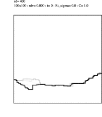
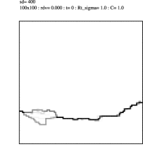
To validate further the claim we carried out the following numerical experiment: we first computed the path in a few UC arrays. Keeping everything else the same, we introduced disorder in the tunneling resistances in the otherwise similar arrays and computed the paths. For the four different arrays we experimented with, we did not find any significant changes in the structure of path (although actual values of the current densities will be different). Fig. 33 shows the results for one of them. Although not conclusive, this is indicative that resistance disorder at most changes the current density distribution for a given sample and that change is indistinguishable when averaged over many samples. It is important to mention that the ground state paths in Fig. 33 and similar experiments, were not computed using the transfer-matrix approach, but was dynamically determined at . It is possible, however, that due to greater dynamical freedom in selecting current flow paths at higher values of , there still be differences in the properties of current carrying paths.
VII Summary and Conclusions
Using computer simulations we can easily control the presence of different disorder types and thus discern the individual and collective effects. In doing so, we find that the presence of background charge disorder is the dominant type of disorder, and although there are some minor changes for arrays with variable capacitance and tunneling disorder, the main scaling arguments and exponents characterizing the arrays at and in the conducting regime close to remain unchanged. A study of the interface properties in section III indicated that the ground-state path for two-dimensional QDA should belong to the same universality class as the DPRM. By looking at the structure and the transverse deviations of the ground-state path we were able to establish the connection conclusively. We also saw in sections II and IV that the introduction of disordered does not change the current-scaling exponents for one-dimensional arrays nor of the ground-state paths. From section V, it appears that the scaling exponent for 2D arrays does not depend upon the types of disorder simulated either.
The dominance of charge disorder is probably due to the fact that the disorder energy scale is set by the presence of the background charge impurities, is the crucial energy scale of the system. This in part is due to the fact that the fluctuation between the charging energy of dots as a consequence of the particular parameter values we choose ( = 2.0), is less than the fluctuation in electrostatic energy due to offset charges being chosen randomly between [0,1[. The presence of tunneling disorder does not change the energetics of the arrays, i.e., and fluctuations in . It is important to remark, however, that if the offset-charge impurities were disregarded and only a non-uniform considered, the arrays would still exhibit a threshold voltage, separating the insulating and conducting phases and most properties would still be similar to the situation where there was only offset-charge impurities. If the energy fluctuations due to of non-uniform , was greater than the background charges the claim would be that the dominant form of disorder was the although the properties of the array would be essentially insensitive to which was the dominant disorder.
From our discussion in section [V], we make the important conclusion that it is most likely that the MW hypothesis is correct and valid for disordered QDA irrespective of the actual relative strengths of the disorder. It is important to appreciate that one needs to get sufficiently close to threshold to observe the scaling and that too only for large systems.
From our experience, a naive approach to determining the steady state current consistently underestimated the current values, which tends to get more acute at lower values of . As a consequence, a higher putative value of would be observed. It also follows that there is a need for careful simulations, for with slightly less diligence it would have been tempting to predict an exponent range of 2.0-2.25. This is intertwined with the issue of high computational cost, which arises from a combination of the need to compute the converged current accurately for a single sample and the need to simulate large systems as a consequence of strong finite-size effects. It is not easy to formulate an elegant algorithmic solution to this problem. Although, parallelization is a well defined and often used approach to reduce time-to-solution of a problem, our problem does not appear to be a suitable candidate, for as mentioned, one of the primary bottlenecks in our simulations is the extremely long times required to reach a steady-state configuration. It is physically-meaningless to run a simulation at a time without state information at time , where is a time later than time ; thus there is a fundamental limitation on speed-up that can be achieved via parallelization. But parallelization possibly along the lines of Ref. [Korniss et al., 2000] may be a possible route forward.
We have focused on QDA in the extreme limit where the screening-length is less than the spacing between dots. The opposite regime of essentially infinite screening-length has been well studied, both numerically and theoretically for non-disordered arrays Bakhalov et al. (1989) and recently for arrays with a random background potential Kaplan et al. (2003) – although neither of these studies, nor others that we are aware of, use the statistical physics approach that we have used. Surprisingly, there has been little activity in the regime representing the middle ground, viz., a screening length from a few upto a dozen dot spacings. With a screening-length more than a single dot spacing, the on-site interaction model that we have used in this work is not valid and computational approaches will require fundamental reworking. Ironically this regime is important (and interesting), as most nanoparticle arrays as a consequence of the absence of an underlying gate most probably have an electrostatic screening-length of a few dot spacings.
In summary, we have investigated the effect of disorder on the transport of electrons in arrays of mesoscopic sized metallic islands, at, below and above a critical voltage . In contrast to experiments, using computer simulations we can easily control the effects of different disorder types. We find that the presence of background charge disorder is the dominant type of disorder and although there are some minor changes with the addition of variable capacitance and tunneling disorder, the main scaling arguments and exponents characterizing the arrays at threshold and in the conducting regime remain unchanged. Our numerical results indicate a value for the exponent to be in the range 1.5-2.0.
Acknowledgements.
One of us (SJ) would like to thank Dave McNamara for helpful discussions during the initial stages of the work. This work was supported in part by the National Science Foundation DMR-0109164.References
- Berven et al. (2002) C. A. Berven, M. N. Wybourne, L. Clarke, L. Longstreth, J. E. Hutchison, and J. L. Mooster, Journal of Applied Physics 92, 4513 (2002).
- Kurdak et al. (2000) C. Kurdak, A. J. Rimberg, T. R. Ho, J. Clarke, and J. D. Walker, Physica E 5, 274 (2000).
- Kouwenhoven et al. (1997a) L. P. Kouwenhoven, G. Schon, and L. Sohn, Mesoscopic Electron Transport (Kluwer Academic, 1997a), chap. 1.
- Kouwenhoven et al. (1997b) L. P. Kouwenhoven, C. M. Marcus, P. L. McEuen, S. Tarucha, R. M. Westervelt, and N. S. Wingreen, Electron Transport in Quantum Dots (Kluwer, 1997b).
- Fisher (1998) D. S. Fisher, Physics Reports 301, 113 (1998).
- Fisher (1987) D. S. Fisher, Nonlinearity in Condensed Matter (Springer, New York, 1987), chap. Friction and Forced Flow: Collective Transport in Disordered Media.
- Duruoz et al. (1995) C. I. Duruoz, R. M. Clarke, C. M. Marcus, and J. S. Harris, Phys. Rev. Lett. 74, 3237 (1995).
- Enomoto (1999) Y. Enomoto, Physica B 272 (1999).
- Granato and Kosterlitz (1999) E. Granato and J. Kosterlitz, Phys. Rev. Lett. 81, 3888 (1999).
- Hirasawa et al. (1998) M. Hirasawa, S. Katsumoto, A. Endo, and Y. Iye, Physica B 252-256, 249 (1998).
- Parthasarathy et al. (2001) R. Parthasarathy, X.-M. Lin, and H. M. Jaeger, Phys. Rev. Lett. 87, 186807 (2001).
- Parthasarthy et al. (2004) R. Parthasarthy, X. Lin, K. Elteto, T. Rosenbaum, and H. M. Jaeger, Phys. Rev. Lett. 92, 076801 (2004).
- Kurdak et al. (1998) C. Kurdak, A. J. Rimberg, T. R. Ho, and J. Clarke, Phys. Rev. B 57, R6842 (1998).
- Rimberg et al. (1995) A. J. Rimberg, T. R. Ho, and J. Clarke, Phys. Rev. Lett. 74, 4714 (1995), e-print.
- Ancona et al. (2001) M. G. Ancona, W. Kruppa, R. W. Rendell, A. W. Snow, D. Park, and J. B. Boos, Physical Review B 64, 033408 (pages 4) (2001), eprint.
- Middleton and Wingreen (1993) A. A. Middleton and N. S. Wingreen, Phys. Rev. Lett. 71, 3198 (1993).
- Kaplan et al. (2003) D. M. Kaplan, V. A. Sverdlov, and K. K. Likharev, Phys. Rev. B 68, 045321 (2003), eprint.
- Melsen et al. (1997) J. A. Melsen, U. Hanke, H.-O. Muller, and K. A. Chao, Phys. Rev. B 55, 10638 (1997).
- Johansson and Haviland (2001) J. Johansson and D. Haviland, Phys. Rev. B 63, 014201 (2001).
- Berven and Wybourne (2001) C. A. Berven and M. N. Wybourne, Applied Physics Letters 78, 3893 (2001).
- Averin and Likharev (1991) D. V. Averin and K. K. Likharev, Mesoscopic Phenomena in Solids (Elseivier Publications, 1991), chap. chapter 5.
- Bezryadin et al. (1999) A. Bezryadin, R. M. Westervelt, and M. Tinkham, Applied Physics Letter 74, 2699 (1999), e-print.
- Bray and Moore (1987) A. J. Bray and M. A. Moore, Phys. Rev. Lett. 58, 57 (1987), eprint.
- Fisher (1984) M. Fisher, Journal of Statistical Physics 34, No (5/6) (1984).
- Kinnison (TBD) R. R. Kinnison, Applied Extreme Value Statistics (TBD, TBD).
- Watson and Fisher (1996) J. Watson and D. S. Fisher, Phys. Rev. B 54, 938 (1996).
- Bassler et al. (2000) K. E. Bassler, M. Paczuski, and E. Altshuler, Los Alamos e-print Archive cond-mat/0009278 (2000).
- Narayan and Middleton (1994) O. Narayan and A. A. Middleton, Phys. Rev. B 49, 244 (1994).
- Middleton and Fisher (1993) A. A. Middleton and D. S. Fisher, Phys. Rev. B 47, 3530 (1993).
- Jha (2004) S. Jha, Ph.D. thesis, Department of Physics, Syracuse University (2004).
- Barabasi and Stanley (1995) A. L. Barabasi and H. E. Stanley, Fractal Concepts in Surface Growth (Cambridge University Press, 1995).
- Surdeanu (1999) R. Surdeanu, Phys. Rev. Lett. 83, 2054 (1999).
- Maunuksela (1997) J. Maunuksela, Phys. Rev. Lett. 79, 1515 (1997).
- Alava and et al (2000) M. Alava and M. M. et al, Phys. Rev. Lett. 84, 1946 (2000).
- Family and Vicsek (1985) F. Family and T. Vicsek, J. Phys. A L75 (1985).
- Roux et al. (1991) S. Roux, A. Hansen, and E. L. Hinrichsen, J. Physics A 25, L295 (1991).
- Martys et al. (1991) N. Martys, M. Cieplak, and M.O.Robbins, Phys. Rev. Lett. 66, 1058 (1991).
- Faleski et al. (1996) M. C. Faleski, M. C. Marchetti, and A. A. Middleton, Phys. Rev. B 54, 12427 (1996).
- Watson and Fisher (1997) J. Watson and D. S. Fisher, Phys. Rev. B 55, 14909 (1997).
- Narayan and Fisher (1994) O. Narayan and D. Fisher, Phys. Rev. B 49, 9469 (1994).
- Thorne (1996) R. E. Thorne, Physics Today pp. 42–47 (1996).
- Goldenfeld (1992) N. Goldenfeld, Lectures on PPhase Transitions and the Renormalization Group (Addison Wesley, 1992).
- Binder and Landau (2000) K. Binder and D. Landau, A Guide to Monte Carlo Simulations in Statistical Physics (Cambridge University Press, 2000), chap. 4.
- Korniss et al. (2000) G. Korniss, Z. Toroczkai, M. A. Novotny, and P. A. Rikvold, Phys. Rev. Lett. 84, 1351 (2000).
- Bakhalov et al. (1989) N. S. Bakhalov, G. S. Kazacha, K. K. Likharev, and S. I. Serdyukovad, Sov. Phys. JETP 68(3), 581 (1989).