Direct evidence for ferroelectric polar distortion in ultrathin lead titanate perovskite films
Abstract
X-ray photoelectron diffraction is used to directly probe the intra-cell polar atomic distortion and tetragonality associated with ferroelectricity in ultrathin epitaxial PbTiO3 films. Our measurements, combined with ab-initio calculations, unambiguously demonstrate non-centro-symmetry in films a few unit cells thick, imply that films as thin as 3 unit cells still preserve a ferroelectric polar distortion, and also show that there is no thick paraelectric dead layer at the surface.
pacs:
77.80.-e, 61.14.Qp, 77.55.+fI Introduction
Theoretical developments and novel experiments in the area of ferroelectrics have rapidly evolved over the last ten years, allowing further progress in the understanding of this remarkable phenomenon. In particular, “nanoscale” ferroelectrics have attracted considerable attention ahn04_1 ; lee05 ; was04 ; chu04 ; nau04 . The question of the existence of a critical thickness, in other words whether or not ferroelectricity can be maintained at reduced dimensions, is amongst the most exciting topics of the field today, with very active experimental tyb99 ; str02 ; fon04 ; lic05 and theoretical efforts gho00 ; mey01 ; jun03_1 .
Probing ferroelectricity in thin films and nanostructures is a difficult task, which requires advanced techniques. Among these, scanning probe characterization based on piezoelectric microscopy has allowed a ferroelectric ground state to be identified down to 40 Å in thin Pb(Zr0.2Ti0.8)O3 films tyb99 , and x-ray studies on PbTiO3 films suggested that 28 Å films are ferroelectric lic05 . Dielectric and pyroelectric response measurements have allowed ferroelectricity to be identified in polymer films down to 10 Å (two unit cells) bun98 . More recently, ultrahigh vacuum scanning probe characterization based on electrostatic force microscopy was used to study ferroelectricity in barium titanate nanowires with diameters as small as 10 nm yun02 . On insulating substrates, lateral periodicity was observed via x-ray diffraction in thin PbTiO3 films down to 12 Å and attributed to alternately polarized domains str02 ; fon04 . In all these studies, however, properties averaged over the complete ferroelectric structure were measured and no local information on the atomic displacements was obtained.
In contrast, the photoemission based photoelectron diffraction (XPD) used in our study presents two interesting characteristics: it is naturally surface sensitive, due to an electron escape depth of approximately 20 Å (at the energy used here) ; and atomic displacements within the unit cell can be directly probed, allowing the non-centro-symmetric and tetragonal nature of the crystal lattice to be directly demonstrated. This turns out to be crucial for studying ultrathin films, and for discriminating the behavior of the surface from that of the body of the film.
The paper is organized as follows. In Section II, we characterize the ferroelectric distortion of PbTiO3 and contrast it to the natural atomic relaxation appearing at surface and interface. In Sec. III A, we discuss aspects of the measurement methods while, in Sec. III B we show the non-centro-symmetry of a 20 Å thick film using XPD. The Sec. III C is dedicated to the tetragonality measurements as a function of film thickness with XPD using Pb as emitter, down to 4 Å (one unit cell). We summarize and conclude in Sec. IV.
II Ferroelectric distortion versus surface relaxation
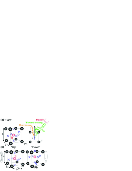
The studies were carried out on c-axis oriented perovskite PbTiO3 ultrathin films epitaxially grown on conducting Nb-SrTiO3 substrates. Above 490∘C, bulk PbTiO3 is a paraelectric insulator and a simple cubic perovskite structure with a lattice parameter of 3.96 Å (“para”-state, see Fig. 1(a)). In this structure, the Ti and O atoms are in perfectly centro-symmetric positions with respect to the surrounding Pb cage. At lower temperature, the material becomes tetragonal and ferroelectric with a- and c-axis parameters of 3.90 Å and 4.17 Å, respectively nel85 ; jon97 , as illustrated in Fig. 1(b). The ferroelectric phase is characterized by a non-centro-symmetric structure where the O and Ti atoms are unequally shifted with respect to Pb. In a unit cell with the polar c-axis along the -direction, O and Ti move either upwards or downwards (with a larger O displacement) resulting respectively in a “down”- and “up”-polarized state, as drawn in Fig. 1(b).
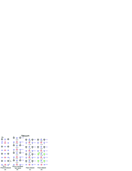
In the surface region (five top unit cells) that is probed by the XPD technique, the evidence of such a polar atomic distortion could be the signature of a ferroelectric “up”- or “down”-state but may also arise from the natural atomic relaxation at the film surface and interface already present in the paraelectric phase. A proper interpretation of our data therefore requires independent quantification of both effects. To that end, a reference configuration (“para-unrelaxed”) is defined in Fig. 2(a): it corresponds to the truncated bulk paraelectric structure of PbTiO3 with the in-plane lattice constant constrained to that of SrTiO3 ( Å) and a consequent tetragonality lic05 . Fig. 2(b) (“ferro-unrelaxed”) shows the atomic distortion of the “up”-state as determined for bulk tetragonal PbTiO3 by Nelmes and Kuhs in Ref. nel85 with Å. In order to quantify the surface relaxation, density functional theory calculations abinit were performed within the local density approximation (LDA) using the ABINIT gon02 package. Two different supercells were considered : a thick PbTiO3 slab in vacuum (Fig. 2(c)) and a SrTiO3/(one unit cell) PbTiO3/vacuum stack unitcell (Fig. 2(d)). Insulating SrTiO3 was considered in our simulations since Nb doping is not presently affordable at the first-principles level STO . To reproduce the substrate clamping effect, the in-plane lattice constant was fixed to the relaxed a-axis value of bulk SrTiO3 acell . The atomic positions were then relaxed until the maximum residual atomic force was smaller than 40 meV/Å. Our calculations were restricted to surface periodicity and did not allow for an eventual antiferrodistortive (AFD) reconstruction bun05 ; sep05 . The latter is not excluded but, as discussed later, was not evidenced on our films at room temperature. The distortions in the upper half of each supercell are reported in Fig. 2(c), (d) (“para-relaxed” state). For easy comparison with the experiment, because of the typical LDA underestimate of the lattice constant acell , the values are given as a percentage of . The magnitudes of the ferroelectric and surface relaxation effects can now be compared. First, the cation-oxygen displacements due to ferroelectricity (11.6% - 8.3% of , Fig. 2(b)) are significantly larger than the displacements due to surface relaxation/rumpling (3.4% - 1.4% of , Fig. 2 (c) and 3.3% - 1.5% of , Fig. 2(d)). Second, the mean layer displacement for the “up”-state (Fig. 2(b)) and for the surface relaxation (Figs. 2, (c) and (d)) are opposite. Third, the surface relaxation and rumpling effects are globally unaffected by the film thickness (Figs. 2, (c) and (d)) and their amplitude decays very quickly in the interior of the film : they are already negligible two unit cells below the surface. This implies that the XPD measurements will be probing both the narrow relaxed surface region and a few unit cells below, essentially not affected by the surface relaxation.
III Experimental results and discussion
III.1 Experimental details
The samples used in this study are epitaxial, c-axis oriented PbTiO3 thin films grown on conducting (001) Nb-SrTiO3 substrates using off-axis radio-frequency magnetron sputtering eom90 ; lic04 . Topographic measurements using atomic force microscopy (AFM) showed that these films are essentially atomically smooth, with a root-mean-square roughness between 2 and 6 Å over a 10 10 m2 area. Room temperature x-ray diffraction measurements, for films with thickness 28 Å allowed us to precisely determine the thickness and the c-axis parameter of the films, and to confirm their epitaxial “cube-on-cube” growth.
After growth and characterization, the films were transferred ex-situ to a modified Vacuum Generators ESCALAB Mk II photoelectron spectrometer. The XPD measurement system comprises a hemispherical electron energy analyzer with a three-channel detector, an x-ray photon source with two possible energies ( = 1253.6 eV and 1740 eV for MgK and SiK radiation, respectively), and a computer-controlled two-axis goniometer capable of rotating the photoelectron emission angle over the full hemisphere above the surface ost91 ; nau93_1 .
The local geometry around a selected atom can be probed by performing an intensity versus emission-angle scan of a chosen photoemission line. Because of the chemical sensitivity of photoemission, a given atom type is then chosen by selecting one of its core levels. The outgoing photoemitted electrons exhibit a strongly anisotropic angular intensity distribution. This angular distribution is due to the interference of the directly emitted photoelectron wave with the scattered electron waves. The analysis of the interference (or diffraction) patterns is facilitated by the so-called “forward focusing” effect taking place for photoelectron kinetic energies greater than 0.5 keV. When considering a row of atoms, scattering at the first few atoms along this row focuses the electron flux in the emitter-scatterer direction (for a review see Ref. ege90 ; fad90 ). This enhancement of the intensity in the emitter-scatterer direction is schematically illustrated by the green curve in Fig. 1(a) (right part) for the centro-symmetric “para”-state (continuous line) and the “up”-state (dotted line). The forward focusing effect is further amplified for electron scattering by heavy atoms. In a semi-classical picture this can be understood as the focusing of the electron wave by the high number of protons in high atomic number atoms ege90 . Note that, despite the forward focusing effect, the experimentally measured angles are sensitive to multiple interferences, refraction and possible anisotropic atom vibrations at the surface. In the present case of PbTiO3, Pb scattering is highly dominant compared to the scattering by other elements des05 . As a first step, in order to probe the non-centro-symmetry, O was chosen as emitter-atom (O 1s core level, Ekin = 724.1 eV), since it has the largest displacement nel85 and has Pb scatterers as nearest neighbors (see Fig. 3). However, the O contribution from the Nb-SrTiO3 substrate becomes non-negligible for films thinner than the photoelectron inelastic mean free path, making the study of films thinner than 20 Å more difficult. As a second step, in order to probe the tetragonality of the films, i. e., the ratio of the Pb lattice (related to the polarization via the polarization-strain coupling as discussed below and in details in Ref. lic05 ), Pb was chosen as emitter-atom (Pb 4f7/2 core level, Ekin = 1115.5 eV), and Pb-Pb forward focusing directions were used. Since Pb atoms are absent from the substrate, this study can be done down to a monolayer of ferroelectric material.
III.2 Non-centro-symmetric position of oxygen atoms
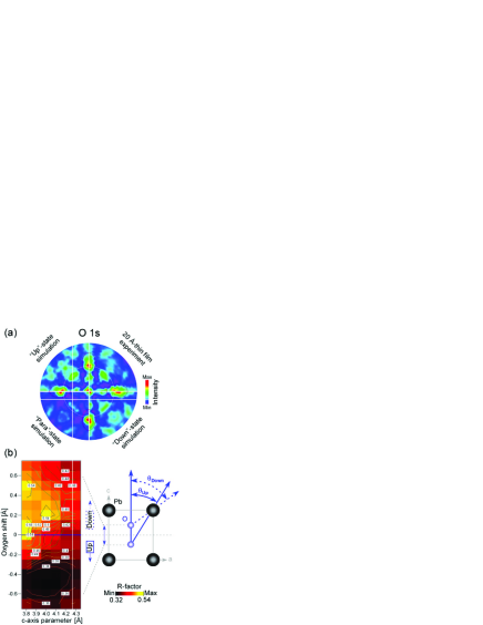
First, considering oxygen as the emitter atom, fully automated computer code for calculating electron diffraction in atomic clusters (EDAC) via multiple scattering gar01 , based on the muffin-tin potential approximation pen74 was used to calculate the XPD pattern. Fig. 3(a) shows four O 1s core level emission (Ekin = 724.1 eV) interference patterns. One is the measurement made on a 20 Å thin film while the three others are multiple scattering EDAC calculations of the “up”-, “down”- and “para”-state. Intensities are plotted in a stereographic projection with the center corresponding to normal emission (polar angle ) and the outer border corresponding to grazing emission (). The strongest intensities (surrounded by red ellipses) correspond to the scattering of O 1s photoelectrons by Pb nearest neighbours (see Fig. 3(b)). The white circle is a guide to the eye indicating the polar angle of maximum intensity for the measured interference pattern. It is evident that the polar angle position of this peak, which is directly linked to the O-Pb directions, is perfectly reproduced by the “up”-state calculation while the “para”- and the “down”-state simulations predict a different position. The “up”-state (down-shifted O position) corresponds to a smaller polar emission angle ( in Fig. 3(b)) appearing closer to normal emission (center of the interference pattern in Fig. 3(a)). Such measurements have also been performed on films with thicknesses of 500, 200, 100, 60, 44 and 28 Å, and all perfectly reflect the characteristics of the “up”-state 111The presence of alternating 180∘ domains in our films can be ruled out from the XPD measurement because the two characteristic “up” and “down”-state “forward focusing” peaks are not observed simultaneously in the experimental diffractogram, Fig. 3(a). This contrasts with the results of Fong et al. fon04 on a insulating substrates..
These conclusions, drawn from visual inspection of the interference patterns locally around the intensity maximum (Fig. 3(a)), are confirmed by a global matching approach using a reliability (R)-factor to evaluate the quality of the fit between the complete experimental interference pattern data and theory (Fig. 3(b)). The c-axis lattice constant value and the O and Ti shifts are the adjustable structural parameters. A cut in the (100) plane, containing Pb and O atoms, is shown to facilitate the discussion. In the calculation, O and Ti atoms are moved together and the dipole is continuously changed from the “down”-state to the “up”-state, crossing over the “para”-state. The best fit corresponds to the minimal R-factor value, which is reached when O and Ti atoms are shifted below the centro-symmetric position (parameters used for the “up”-state simulation in Fig. 3(a)), with an R-factor value of 0.34. In comparison, for the same c-axis parameter but the opposite O and Ti atom shifts (parameters used for the “down”-state simulation in Fig. 3(a)), the calculation gives a much higher R-factor of . In between (zero O shift), in the centro-symmetric “para”-state, the R-factor is (parameters used for the “para”-state simulation in Fig. 3(a)).
It is important to note that surface relaxation and rumpling, neglected here, cannot weaken our conclusions; indeed they would give a picture resembling a “down”-state, the corresponding O-Pb atoms being shifted in the opposite direction than what is observed (see Fig. 2(c)). Also, the possibility of a surface AFD reconstruction was explored without finding evidence for it in our room temperature experiments.
This R-factor analysis therefore quantitatively confirms the observations made in Fig. 3(a), namely that the measured interference pattern is best simulated with the “up”- state. This demonstrates unambiguously that, for a film as thin as 20 Å the O atoms have a non-centro-symmetric position in the Pb cage corresponding to a non-vanishing spontaneous polarization.
Let us emphasize that piezoelectric AFM measurements performed after the XPD experiments on the thickest films ( 500 Å) confirmed the uniform“up”-state polarization while a uniform “down”-state polarization had been initially found for the same films just after growth. This confirms the monodomain character of the as grown sample and also indicates that the films are uniformly switched from “down” to “up”-state by exposure to our conventional x-ray source, attesting for the switchable character of the polarization. The details behind the switching are presently not known, but we believe that it occurs at the initial stage of the experiment while the measurement itself is essentially done in zero field. In fact, our results do not depend on the x-ray intensity, proving that the films are in equilibrium state during the measurements 222The influence of the x-ray intensity on the tetragonality was measured by investigating different x-ray powers. A modification of the tetragonality would have indicated, via the polarization-strain coupling, a variation of the spontaneous polarization. However no such modification was found.. As discussed below, the agreement between the tetragonality deduced from x-ray diffraction and XPD also suggests that the measurements are performed in similar conditions.
III.3 Tetragonality via lead emission
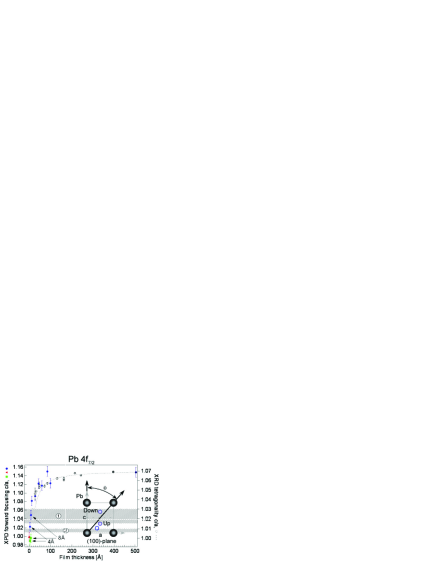
In a second step, considering Pb as the emitter atom, XPD was used to determine the tetragonality. As demonstrated in Ref. lic05 , below 200 Å the tetragonality decreases as the film thickness decreases. This decrease is a consequence of the strong polarization-strain coupling in PbTiO3 and a signature of a reduced polarization in thin films. In Ref. lic05 , this polarization reduction was attributed to imperfect screening of the depolarizing field jun03_1 . With XPD, using Pb as emitter, the tetragonality was measured down to the unit cell level as shown in Fig. 4. The absolute values of , deduced from the forward focusing angles, are particulary large. This might reflect a strong enhancement of the polarization in the probed surface region (of the order of for , from the PTO polarization-strain coupling), even larger than in the theoretical prediction of Ref. gho00 . However, as previously stated, we are not necessarily measuring the precise atom-atom directions and the anomalously large forward focusing might also be related to other effects (anisotropic atom vibrations at the surface, refraction and multiple scattering interferences). Therefore a comparison with x-ray diffraction (XRD) lic05 must be done at the relative level (Fig. 4, left and right scale).
To study the evolution of the tetragonality as a function of the film thickness, the measured XPD values are compared to the values obtained by XRD. The XPD measurement on Fig. 4 confirms the evolution of c/a obtained from x-ray measurements in Ref. lic05 and agrees with the theoretical prediction (dashed curve) relying on the suppression of polarization due to imperfect screening of the depolarizing field lic05 . The similar thickness dependence for the XPD (very surface sensitive) and the x-ray measurements (average on the whole film) implies that the polarization evolves at the surface in the same way as at the interior of the film and that there is no thick paraelectric dead layer at the surface. In addition, the XPD tetragonality measurement shows a continuous decrease of tetragonality down to the thickness of one unit cell unitcell . Two ribbons are drawn in Fig. 4, labeled with 1 and 2. They indicate the regions within which values of 1.03 and 1.01 are crossed with respect to both c/a scales. For film thicknesses above two unit cells, the values are larger than 1.03, the value expected at the bulk level for the paraelectric phase (resulting from the mechanical constraint imposed by the substrate, see also Fig. 2(a)). This observation directly implies, via the polarization-strain coupling, that the films still have a finite -although progressively reduced- spontaneous polarization. At thicknesses of one or two unit cells, as can be seen on Fig. 4, c/a drops even more, reaching a value close to 1.01 for the one unit cell thick film unitcell . This further decrease highlights that macroscopic elasticity no longer applies at such thicknesses where the interlayer atomic distances are affected by surface relaxation and rumpling as shown by the ab-initio calculations (Fig. 2(d)). The measured tetragonality agrees with the computed value of 1.01 for the one unit-cell thick relaxed paraelectric film suggesting the absence of any additional ferroelectric distortion at this thickness.
IV Conclusion
This study thus directly demonstrates non-centro-symmetry, unambiguously a result of ferroelectricity in PbTiO3 thin films down to 20 Å. The measurements of the tetragonality, with a continuous decrease down to the bare substrate, show that even extremely thin films (3 unit cells) have a value larger than 1.03, attesting for the presence of a non-vanishing spontaneous polarization at this thickness scale. As the film thickness is reduced to a single unit cell, the experiments, together with calculations, strongly suggest that both non-centro-symmetry and tetragonality are governed by surface effects, giving rise for our geometry to a polar relaxed structure but without switchable ferroelectric distortion.
Acknowledgements
We would like to thank M. A. Van Hove and C. Battaglia for helpful discussions, P. Paruch for careful reading of the manuscript, and the whole Neuchâtel workshop and electric engineering team for efficient technical support. This project has been supported by the Swiss National Science Foundation through the National Center of Competence in Research “Materials with Novel Electronic Properties-MaNEP”, the European Network of Excellence FAME and the VolkswagenStiftung.
References
- (1) C. H. Ahn, K. M. Rabe, and J.-M. Triscone, Science 303, 488 (2004).
- (2) H. N. Lee et al., Nature 433, 395 (2005).
- (3) R. Waser and A. Rüdiger, Nature Materials 3, 81 (2004).
- (4) M.-W. Chu et al., Nature Materials 3, 87 (2004).
- (5) L. B. I. I. Naumov and H. Fu, Nature (London) 432, 737 (2004).
- (6) T. Tybell, C. H. Ahn, and J.-M. Triscone, Appl. Phys. Lett. 75, 856 (1999).
- (7) S. K. Streiffer et al., Phys. Rev. Lett. 89, 067601 (2002).
- (8) D. D. Fong et al., Science 304, 1650 (2004).
- (9) C. Lichtensteiger, J.-M. Triscone, J. Junquera, and P. Ghosez, Phys. Rev. Lett. 94, 047603 (2005).
- (10) P. Ghosez and K. M. Rabe, Appl. Phys. Lett. 76, 2767 (2000).
- (11) B. Meyer and D. Vanderbilt, Phys. Rev. B 63, 205426 (2001).
- (12) J. Junquera and P. Ghosez, Nature 422, 506 (2003).
- (13) A. Bune et al., Nature (London) 391, 874 (1998).
- (14) W. S. Yun, J. J. Urban, Q. Gu, and H. Park, Nano Letters 2, 447 (2002).
- (15) R. J. Nelmes and W. F. Kuhs, Solid State Commun. 54, 721 (1985).
- (16) F. Jona and G. Shirane, Ferroelectrics Crystals (Dover Publication, New York, 1997).
- (17) Teter norm conserving pseudopotentials were used with Pb (5d, 6s, 6p), Sr (4s, 4p, 5s), Ti (3s, 3p, 3d, 4s) and O (2s, 2p) treated as valence states, a plane-wave energy cutoff of 35 Ha and 6x6x1 k-point sampling of the Brillouin zone.
- (18) X. Gonze et al., Computational Materials Science 25, 478 (2002).
- (19) Note that a film with thickness of one unit cell corresponds to two Pb-O and one Ti-O layers.
- (20) The Nb doping should have a minor effect on the relaxation at the paraelectric level except for ultrathin films for which the metallic character of the surface could allow a larger polar relaxation of the PbTiO3 surface.
- (21) At the bulk level, the calculations provide very similar theoretical in-plane lattice constant for cubic paraelectric SrTiO3 (Å) and tetragonal ferroelectric PbTiO3 (Å, Å) in spite of a global underestimate of the experimental value (Å) typical of the LDA.
- (22) C. Bungaro and K. M. Rabe, Phys. Rev. B 71, 0305420 (2005).
- (23) M. Sepliarsky, M. Stachiotti, and R. L. Migoni, Cond. Mat 0503524 (2005).
- (24) C. B. Eom et al., Physica C 171, 354 (1990).
- (25) C. Lichtensteiger and J.-M. Triscone, Int. Ferroelectrics 61, 143 (2004).
- (26) J. Osterwalder, T. Greber, A. Stuck, and L. Schlapbach, Phys. Rev. B 44, 13764 (1991).
- (27) D. Naumović et al., Phys. Rev. B 47, 7462 (1993).
- (28) W. F. Egelhoff Jr., Critical Reviews in Solid State and Materials Sciences 16, 213 (1990).
- (29) C. S. Fadley, Synchrotron Radiation Research: Advances in Surface Science (Plenum, New York, 1990).
- (30) L. Despont and P. Aebi, to be published.
- (31) F. J. Garcia de Abajo, M. A. Van Hove, and C. S. Fadley, Phys. Rev. B 63, 075404 (2001).
- (32) J. B. Pendry, Low Energy Electron Diffraction (Acamedic Press, London, 1974).