Self-aligned carbon nanotube transistors with charge transfer doping
Abstract
This letter reports a charge transfer p-doping scheme which utilizes one-electron oxidizing molecules to obtain stable, unipolar carbon nanotube transistors with a self-aligned gate structure. This doping scheme allows one to improve carrier injection, tune the threshold voltage Vth, and enhance the device performance in both the “ON-” and “OFF-” transistor states. Specifically, the nanotube transistor is converted from ambipolar to unipolar, the device drive current is increased by 23 orders of magnitude, the device OFF current is suppressed and an excellent ION/IOFF ratio of 106 is obtained. The important role played by metal-nanotube contacts modification through charge transfer is demonstrated.
Significant progress has been made recently on carbon nanotube (CNT) based field effect transistors (FET), both in terms of their fabrication and the understanding of their performance limits.1,2,3 Nevertheless, there are still key issues to be addressed. In particular, there has been no fabrication process-compatible doping method for CNTs. Unlike doping of metal-oxide-semiconductor (MOS) FETs, CNTFETs cannot be doped substitutionally via ion implantation which destroys the CNT lattice. Instead, the quasi one-dimensional (1D) CNTFETs can be doped via charge transfer processes. Benefiting from the weak screening, doping of 1D structures can be more efficient than in 3D devices (e.g., in MOSFETs).4 Current methods used to obtain p- or n- CNTFETs suffer from severe process limitations: for example, a p-CNTFET can be converted to an ambipolar or an n-FET under vacuum pumping through the change of the oxygen content at the metal-CNT interface.5 Efforts utilizing exposure to gas-phase NO26 or trifluoro-acetic acid (TFA)7 to obtain p-CNTFETs require a controlled environment to prevent dopant desorption, and the devices degrade quickly upon exposure to air. Performance-wise, the Schottky barriers (SB) formed between the CNT and the source/drain metal contacts lead to contacts-dominated switching, 8 to a large subthreshold swing S=dVgs/d(log Id), where Vgs is the gate voltage and Id is the drain current, and to strong ambipolar conduction when the transistor is scaled down vertically, i.e., when the gate insulator is thinned substantially. The resulting SB-limited drive current (ION), the slow switching, and exponentially increasing OFF current (IOFF) with increasing drain field9 are unacceptable in logic gate applications. To make CNTFETs technologically viable, it is therefore crucial to find doping methods and materials that both are fabrication process stable and meet the performance challenges. Here we report on a chemical p-doping scheme utilizing oxidizing molecules and a charge transfer mechanism to obtain self-aligned, air-stable, unipolar CNTFETs. We demonstrate the ability to change carrier injection properties; to tune threshold voltage (Vth), and to improve device performance in both ON- and OFF-states.
We have fabricated CNTFETs using laser-ablation-produced CNTs, palladium metal source and drain electrodes separated by 300 nm on top of 10 nm SiO2, and a Si backgate. The substrate with the CNTFETs were then immersed in a dilute solution (0.01 0.1 mg/mL) of triethyloxonium hexachloroantimonate (C2H5)3O+SbCl6- (OA) in methylene chloride or dichlorobenzene. OA is a one-electron oxidant which is known to oxidize aromatic compounds and form charge transfer complexes.10 The interaction of a CNT with this molecule generates a positively charged CNT stabilized by the negatively charged counter ion SbCl6-. If is used to represent the six carbon atom (benzene-like) ring on a CNT, the interaction between the CNT and OA can be represented by Eq. (1):
2 + 3
[(C2H5)3O+SbCl6-]
2 [+.
SbCl6- ] + 3 C2H5Cl + 3
(C2H5)2O + SbCl3 (1)
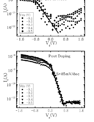
Among the reaction products, C2H5Cl and (C2H5)2O are volatile, while SbCl3 and excess dopants are removed by rinsing with solvents. Typical transistor transfer characteristic curves (Id vs. Vgs) at drain bias (Vds) = -0.1 to -0.5 V at -0.1 V step of a CNTFET before and after doping are shown in Figs. 1(a) and 1(b), respectively. We find (i) Vth for hole conduction increased from -0.7 V (intrinsic CNTFET) to 0.1 V; (ii) the drive current ION improved by 2 orders of magnitude, greatly reducing the contact resistance between tube and metal; (iii) S decreased from 200 to 85 mV/decade, indicating improved switching and a strong reduction of the Schottky barrier; (iv) the transistor transfer characteristic changed from the original ambipolar to pure p-type conduction. After doping, we successfully suppressed the minority carrier (in this case, the electron current) injection at the drain, and obtained excellent drain-induced barrier lowering (DIBL) behavior as is clearly shown from Fig. 1(b). The above results were reproducible with 20 different CNTFET devices stored under nitrogen for weeks. These devices preserve their doping characteristics after solvent washing and vacuum pumping.
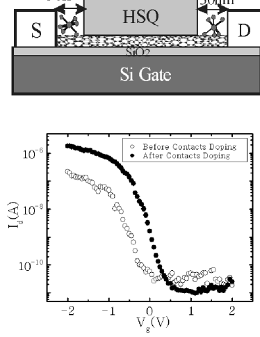
To further understand the dopant-CNT interaction, we selectively doped CNTFETs at the vicinity of the contacts. The negative electron-beam resist hydrogen silsesquioxane (HSQ), which is resistant to the action of the solvents used for doping, was used to mask 200 nm of the CNT channel, leaving a 50 nm unmasked gap at each contact. These open areas were then chemically doped. A cross-section schematic of the device is shown in Fig 2(a). The device transfer characteristics before and after doping are shown in Fig. 2(b). An order of magnitude increase in the drive current is observed, as well as an improvement in S and a 0.5 V increase of Vth. The comparable performance improvements in the case of contacts doping and full-device doping discussed earlier point out the crucial role the contacts play in a SB CNTFET. The simultaneous increase of Ion, decrease of S and the suppression of minority carrier injection [Fig. 1(b)] cannot be explained simply by a carrier concentration increase, as in the case of doping in a conventional MOSFET, where substitutional dopants modify the Fermi level in the bulk of the channel. The improvement in both the device ON- and OFF- states after doping of a CNTFET can, however, be understood in terms of its SB height reduction. The contact barriers were manipulated via the work function modification of the source and drain electrodes under chemical doping. When the OA molecules interact with the electrodes, charge transfer takes place and the stable ions, SbCl6-, remain at the surface of the metal electrodes. They generate an outwards-directed surface dipole that reinforces the intrinsic surface dipole, thus raising the metal workfunction. An increased work function favors hole injection at one electrode (high Ion and low S), while it suppresses electron injection at the other electrode. In fact, modification at the metal-CNT interface band lineup (SB), due to local variation of substrate work function induced by oxygen adsorption, has been observed directly in electrostatic force microscopy (EFM) and scanning Kelvin probe microscopy (SKPM).11 It has also been shown that chemical coadsorption on CNTFETs leads to modified SBs7,11 and can convert a p-type to an ambipolar CNTFET.11 After doping, the device transconductance gm (dId/dVg) at Vds = -1.32 V is 2 S, outperforming those of the best p-CNFET with small diameter CNTs and the same effective gate dielectrics used in our work.
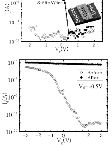
We have demonstrated the reduction of SBs through charge transfer. Ultimately, we need to minimize SBs to the point that transport through a CNTFET is not limited by the contacts; rather by the channel of the tube, as in a conventional MOSFET. In a MOSFET, the gate controls the channel region to overcome its thermionic barrier; whereas in a SB CNTFET, strong gate coupling is crucial to modulate the barriers at the contact regions. In the following experiment, we utilize charge transfer to replace the gate control over the contact regions in a CNTFET, thereby transforming it from a contacts-dominated SB-FET to a channel-controlled FET. To realize this, we exposed part of the channel that is in contact with the metal electrodes to chemical dopants, and used a top gate to individually address each device. A schematic of the device structure is shown in the inset of Fig. 3(a). An initially bottom-gated CNTFET was covered with 12 nm of low temperature oxide (LTO)12 and a tungsten (W) top gate was defined by electron-beam lithography and liftoff. The source/drain separation of the FET was 2 m and the top-gated region was 1.66 m. The patterned W gate was then used as an etch mask to define the 170 nm wide chemical doping windows, formed by removing the LTO with diluted HF, adjacent to the metal contacts. The above process aligns the doping windows with the top-gate in a single patterning step, resembling the “extension doping” of a typical MOSFET.13 This “self-aligned” process allows one to minimize the gate to source/drain capacitive coupling and form completely symmetric source and drain electrodes in a FET, which is crucial in logic applications. To reduce the electrostatic coupling from the bottom gate, the top-gated devices were fabricated on a 100 nm-thick oxide substrate. We do not expect that a SB CNTFET with the above long channel configuration can be either turned on by the weakly coupled top gate or the source/drain fringe fields.14 Indeed, the device remained in its OFF state through a range of applied gate biases, as shown by the open circles in Fig. 3(a). The device cannot be turned ON unless the contact barriers are overcome and enough carriers are induced on the ungated segments. This can be realized by either chemical or electrostatic doping.5,15,16,17 In this work, we adopt the degenerate chemical doping approach to link the source/drain contacts and the bulk of the CNT. Figure 3(b) shows a conventional bottom-gated CNTFET after degenerate doping with OA. The p-CNTFET was converted to an almost metallic CNT which is not modulated by the gate bias. When the device was degenerately doped, carrier density in the CNT was significantly enhanced in addition to the modification of the contacts. Applying this degenerate doping to the top-gated device in Fig. 3(a), we were able to successfully switch it ON and OFF, as shown by the filled circles. After doping, p-type characteristics with a Vth of -0.2 V, a sharp S of 69 mV/dec, and an excellent Ion/IOFF ratio of 106 were obtained. Compared with the fully doped bottom-gated device (Fig. 1), or the the much reduced parasitic capacitance between source/drain and gate in the top gated device (Fig. 3) yields a smaller S, therefore faster transistor switching.
In conclusion, we have demonstrated stable chemical p-doping of CNTFETs, via charge transfer: we improved ION by 23 orders of magnitude, suppressed minority carrier injection and achieved immunity from drain induced IOFF degradation in intrinsic SB CNTFETs, in addition, an excellent ION/IOFF ratio of 106, good DIBL behavior, and a tunable Vth were obtained. Through selective doping we determined that most of the device characteristics improvement came from the dopants interacting with the metal-CNT contacts. Finally, we demonstrated degenerate chemical doping and realized a self-aligned top-gated CNTFET.
The authors thank K. Chan for LTO film deposition, P. Solomon and J. Appenzeller for valuable discussions, and B. Ek for expert technical assistance. C. Klinke acknowledges gratefully the Swiss National Science Foundation (SNF) for their financial support.
1 P. Avouris, MRS Bull. 29, 403 (2004).
2 P. L. McEuen, M. S. Fuhrer, and H. Park, IEEE Trans. Nanotechnol. 1, 78 (2002).
3 A. Javey, Q. Wang, W. Kim, and H. Dai, IEDM Tech. Digest, 2003, p. 31.
4 F. Leonard and J. Tersoff, Phys. Rev. Lett. 83, 5174 (1999).
5 V. Derycke, R. Martel, J. Appenzeller, and Ph. Avouris, Appl. Phys. Lett. 80, 2773 (2002).
6 J. Kong, N. R. Franklin, C. Zhou, M. G. Chapline, S. Peng, K. Cho, and H. Dai, Science 287, 622 (2000).
7 S. Auvray, J. Borghetti, M. F. Goffman, A. Filoramo, V. Derycke, J. P. Bourgoin, and O. Jost, Appl. Phys. Lett. 84, 5106 (2004).
8 J. Appenzeller, J. Knoch, V. Derycke, R. Martel, S. Wind, and Ph. Avouris, Phys. Rev. Lett. 89, 126801 (2002).
9 M. Radosavljevic, S. Heinze, J. Tersoff, and Ph. Avouris, Appl. Phys. Lett. 83, 2435 (2003).
10 R. Rathore, A. S. Kumar, S. V. Lindeman, and J. K. Kochi, J. Org. Chem. 63, 5847 (1998).
11 X. Cui, M. Freitag, R. Martel, L. Brus, and Ph. Avouris, Nano Lett. 3, 783 (2003).
12 S. J. Wind, J. Appenzeller, R. Martell, V. Derycke, and Ph. Avouris, Appl. Phys. Lett. 80, 3817 (2002).
13 S. Wolf, Silicon Processing for the VLSI Era (1990).
14 Y.-M. Lin, J. Appenzeller, and Ph. Avouris, Nano Lett. 4, 947 (2004).
15 S. J. Wind, J. Appenzeller, R. Martel, V. Derycke, and Ph.
Avouris, Appl. Phys. Lett. 80, 3817 (2002).
16 A. Javey, J. Guo, D. B. Farmer, Q. Wang, D. Wang, R. G.
Gordon, M. Lundstrom, and H. Dai, Nano Lett. 4, 447 (2004).
17 Y.-M. Lin, J. Appenzeller, and Ph. Avouris, 62nd Device Research Conference Digest 2004, p. 133.