Contribution of weak localization to
non local transport
at normal metal / superconductor
double interfaces
Abstract
In connection with a recent experiment [Russo et al., Phys. Rev. Lett. 95, 027002 (2005)], we investigate the effect of weak localization on non local transport in normal metal / insulator / superconductor / insulator / normal metal (NISIN) trilayers, with extended interfaces. The negative weak localization contribution to the crossed resistance can exceed in absolute value the positive elastic cotunneling contribution if the normal metal phase coherence length or the energy are large enough.
pacs:
74.50.+r,74.78.Na,74.78.FkI Introduction
The manipulation of correlated pairs of electrons in solid state devices has aroused a considerable interest recently. The goals of this line of research are the realization of sources of entangled pairs of electrons for quantum information, and the realization of fundamental tests of quantum mechanics Choi ; Martin . Correlated pairs of electrons can be extracted from a superconductor by Andreev reflection, with extended or localized interfaces between superconductors and normal metals or ferromagnets Byers ; Deutscher ; Samuelson ; Prada ; Koltai ; Beckmann ; Russo , and in Josephson junctions involving a double bridge between two superconductors Melin-Peysson .
Charge is transported by Andreev reflection at a normal metal / superconductor (NS) interface: an electron coming from the normal side is reflected as a hole while a Cooper pair is transmitted in the superconductor Andreev . In the superconductor, Andreev reflection is mediated by an evanescent state of linear dimension set by the superconducting coherence length . In structures in which a superconductor is multiply connected to normal metal electrodes separated by a distance of order Lambert ; Jedema , the Andreev reflected hole in the spin-() band can be transmitted in an electrode different from the one in which the incoming spin- electron propagates. This “non local” transmission in the electron-hole channel is called “crossed Andreev reflection”. Non local transmission in the electron-electron channel corresponds to “elastic cotunneling” by which an electron is transmitted from one electrode to another while spin is conserved Falci .
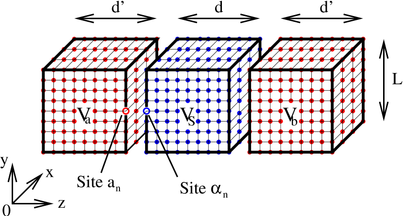
A schematic three-terminal device is represented on Fig. 1, as well as the voltages and applied on the normal electrodes “a” and “b” respectively. The voltage on the superconductor is chosen as the reference voltage (). Non local transport is characterized by a current circulating in electrode “a” in response to a voltage on electrode “b”. It is supposed in addition that : electrode “a” is grounded, like in experiments Beckmann ; Russo (see Fig. 1). The crossed conductance is defined by . A crossed conductance dominated by elastic cotunneling (crossed Andreev reflection) is negative (positive) note-R because of the opposite charges of the outgoing particle in elastic cotunneling and crossed Andreev reflection. Lowest order perturbation theory in the tunnel amplitudes leads to because the crossed Andreev reflection and elastic cotunneling channels have in this case an exactly opposite contribution to the crossed conductance once the average over disorder Feinberg-des ; Cht or over the Fermi oscillations in multichannel ballistic systems Falci ; EPJB is taken into account.
Three unexpected experimental features for the crossed conductance in a normal metal / insulator / superconductor / insulator / normal metal (NISIN) trilayer have been reported recently by Russo et al. Russo : i) The crossed conductance does not average to zero with normal metals, in contradiction to the abovementioned prediction of lowest order perturbation theory in the tunnel amplitudes Falci . The order of magnitude of the experimentally observed crossed signal is far from being compatible with lowest order perturbation theory. ii) A magnetic field applied parallel to the interfaces suppresses the non local signal, suggesting a phase coherent process. iii) The sign of the crossed resistance note-R crosses over from positive (the sign of elastic cotunneling) to negative (the sign of crossed Andreev reflection) as the bias voltage increases, and the crossed signal disappears if the bias voltage exceeds the Thouless energy in the superconductor.
We show here that weak localization with extended interfaces leads to a positive crossed conductance, the sign of which is opposite to the sign of the dominant elastic cotunneling channel for localized interfaces Melin-Feinberg . The weak localization contribution to the crossed conductance becomes important at large bias voltages and for a large phase coherence length in the normal metals.
II Preliminaries
II.1 Hamiltonians
The normal metal electrodes are described by the tight binding Hamiltonian
| (1) |
where is the wave-vector, the projection of the electron spin on the spin quantization axis, and where is the dispersion relation of free electrons on a cubic lattice, with the bulk hoping amplitude, the distance between two neighboring sites, and , and the projections of the electron wave-vector on the , and axis (see Fig. 1).
The superconductor is described by the BCS Hamiltonian
with the superconducting gap.
Diagonal disorder is included Abrikosov , with an elastic mean free path in the normal electrodes of the NISIN trilayer, and in the superconducting electrode. A finite coherence length in the normal electrodes is accounted for by adding phenomenologically an imaginary part to the energy.
At the extended interface -, the tunnel Hamiltonian connecting the electrodes “a” and “” takes the form
| (2) |
where the sites on the normal metal side of the interface correspond to the sites on the superconducting side of the interface (see Fig. 1), and a similar expression holds for the tunnel Hamiltonian at the interface -.
II.2 Green’s functions
The fully dressed advanced and retarded equilibrium Nambu Green’s function at energy is first determined by solving the Dyson equation
| (3) |
where denotes a summation over the spatial indices, and are the advanced and retarded Green’s functions of the disconnected system (i. e. with in the tunnel Hamiltonian given by Eq. (2)). The self-energy corresponds to the couplings in the tunnel Hamiltonian given by Eq. (2). The Green’s functions are matrices in the spin Nambu representation. The four components correspond to a spin-up electron, a spin-down hole, a spin-down electron and a spin-up hole. Because of spin rotation invariance, some elements of the Green’s functions are redundant. We work here in a block in the sector , encoding the superconducting correlations among a spin-up electron (Nambu label “1”) and a spin-down hole (Nambu label “2”).
Once the fully dressed advanced and retarded Green’s functions have been obtained, the Keldysh Green’s function is determined by the Dyson-Keldysh equationNozieres ; Martin-Rodero93 ; Levy95-PRB ; Levy95-JPCM ; Cuevas
| (4) |
where is the Keldysh Green’s function of the isolated electrodes, and where the energy dependence of the Green’s functions is omitted.
II.3 Transport formula
The current through the interface - is given by
where the trace is a summation over the two components of the Nambu Green’s function, is one of the Pauli matrices, the diagonal elements of which are , and the sum over runs over all sites at the interface -. As shown on Fig. 1, the symbols and in Eq. (II.3) label two corresponding sites at the interface, in the normal electrode “a” and in the superconductor respectively. The two spin orientations are taken into account in the prefactor of Eq. (II.3).
The local conductance of a NIN interface is equal to per channel, where is the dimensionless transmission coefficient in the tunnel limit, with the normal density of states Nozieres .
The non perturbative transport formula for the local current at a localized NIN interface was obtained in Ref. Nozieres, , and generalized in Ref. Cuevas, to a localized NIS interface, and in Ref. Melin-Feinberg, to non local transport at a double ferromagnet / superconductor interface. We deduce from these references the exact expressions of the local conductance of a single NIN interface, of the Andreev conductance of a single NIS interface, and of the crossed conductance of a NISIN trilayer with extended interfaces:
valid to all orders in the hopping amplitude. The crossed conductance is per conduction channel through the junction of area , with a superconducting layer of thickness (see Fig. 1). The summations in Eqs. (II.3) and (II.3) run over all pairs of sites at the interfaces, and the overline denotes disorder averaging. The density of states connects the sites and in electrode “a”, and a similar definition holds for . The site () in electrode “a” (“b”) is connected by the tunnel Hamiltonian to the site () in the superconductor (see Fig. 3 for the NISIN interface). In the case of the local conductance of a NIN junction, , , and belong to an insulating layer that has been inserted in between the two normal metals. The tunnel amplitude in Eq. (II.3) connects in this case the normal metal to the insulator, while in Eqs. (II.3) and (II.3) connects the normal metal to the superconductor.
The fully dressed advanced and retarded equilibrium Nambu Green’s functions and at energy in Eqs. (II.3), (II.3) and (II.3) are expanded by using the Dyson equation given by Eq. (4). We deduce from the exact Keldysh transport formula given by Eqs. (II.3), (II.3) and (II.3) that the diagrams are connected, and that the propagators for the density of states are directly connected to at least one tunneling vertex. The other extremity of the density of states propagators is connected either to a tunneling vertex, or to a disorder scattering vertex. The density of states, represented by wavy lines on the diagrams, connects to one advanced and one retarded Green’s function as in Eqs. (II.3), (II.3) and (II.3).
A crossed conductance dominated by elastic cotunneling (crossed Andreev reflection) is negative (positive) note-R . This can be seen most simply by making the Nambu labels explicit in Eq. (II.3) and taking into account the signs in the matrices, and the global sign.
The crossed conductance is expanded perturbatively in , where the normal local transmission coefficient has already been defined, and is also expanded in the number of non local processes crossing the superconductor since Falci .
II.4 Weak localization in a superconductor
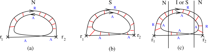
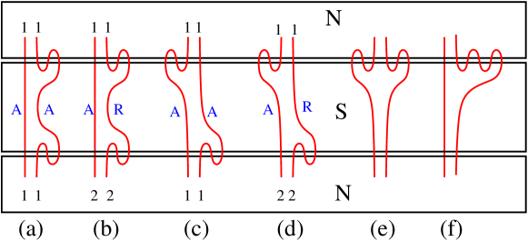
Weak localization in a superconductor was already investigated in Ref. Smith, in connection with the determination of the number density of superconducting electrons. A weak localization diagram in a bulk normal metal is shown on Fig. 2a. In this case the two points and are within the elastic mean free path . In a bulk superconductor (see Fig. 2b), the two points and are within the coherence length since the disorder average of two advanced Green’s functions between the two sites and at and in a superconductor is limited by , not by . Similar diagrams for the conductance are introduced at a NISIN double interface in Sec. III. In this case the points and are separated by the superconductor thickness, of order (see Fig. 2c). At a NIN interface, the two points and on different interfaces can be separated by a distance equal to the thickness of the insulator, comparable to the decay length induced by the charge gap of the insulator.
III Non local transport in a NISIN trilayer
III.1 Crossed conductance to order
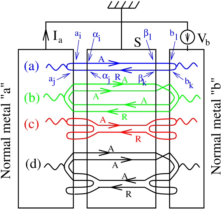
Now we evaluate the lowest order diagrams appearing in the crossed conductance of a NISIN trilayer. The crossed conductance due to the diagram of order (see Fig. 3a) vanishes because the contributions of the elastic cotunneling and crossed Andreev reflection channels are exactly opposite Feinberg-des ; Melin-Feinberg ; Falci ; EPJB . This can be seen also by evaluating the summation over the Nambu labels in the diagram on Fig. 3 and using , where and are two points in the superconductor at a distance of order .
III.2 Crossed conductance to order
The first weak localization diagram of order involving four Green’s functions in the superconductor is shown on Fig. 3b. The corresponding crossed conductance vanishes, as for the diagram of order discussed in Sec. III.1.
The diagram of order on Fig. 3c takes a finite value, and is evaluated explicitely by summing over all possible Nambu labels, and over the different possibilities of inserting the density of states and the matrices (represented by the wavy lines on the diagrams). This leads to the crossed conductance
whereMelin-Feinberg
with the distance between the sites and , and with in the ballistic limit, and in the diffusive limit. The resulting term of order in the crossed conductance is given by
| (10) |
in agreement with the expansion to order of the crossed conductance obtained for highly transparent localized interfacesMelin-Feinberg . A summation over the pairs of sites and at the two interfaces was carried out, giving rise to the prefactor in Eq. (10).
III.3 Weak localization diagram of order
III.3.1 Contribution of local excursions
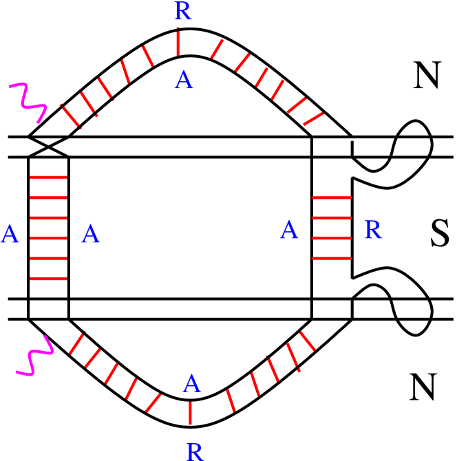
We consider now the weak localization diagram of order on Fig. 3d, merging the features of the two diagrams of order on Figs. 3b and c, and shown in more details on Fig. 4. The long range propagation in the normal electrodes involves the diffusons and in the particle-particle or hole-hole channel (where and belong to the normal electrode), as opposed to the diffuson in the particle-hole channel for local Andreev reflection at a single NIS interface Hekking ; Beenakker below the related Thouless energy.
We first evaluate the part of the diagram on Fig. 4 involving local excursions at the NIS interfaces (see Fig. 5). Enumerating these diagrams shows that the two local excursions are attached to the same non local propagation in the superconductor. We use the notation () for the part of the diagram on Fig. 5 with two advanced (one advanced and one retarded) propagators in the superconductor, and the Nambu labels and at the extremities in the two normal electrodes. We find
| (11) | |||||
| (12) |
We recover Eq. (10) for the non vanishing diagram of order on Fig. 3c, proportional to . The global minus sign in this expression can be found in Eq. (II.3), and the opposite signs for and are due to the matrices in Eq. (II.3). The diagrams with local excursions attached to the disorder average of two advanced or two retarded Green’s functions in the superconductor lead to a vanishingly small crossed conductance, as it can be seen from the identity , deduced from Eq. (11).
III.4 Weak localization crossed conductance
The weak localization contribution to the crossed conductance corresponding to the diagram on Fig. 4 is given by
| (13) |
where is given by Eq. (10) and
The sign of given by Eq. (13) is positive, as for crossed Andreev reflection. The factor is due to a a factor associated to the diffusons in each of the quasi-two-dimensional normal layers [see Eq. (24)] in the limit . The constraint originates from the conservation of the component of the wave-vector parallel to the interface, due to the symmetry by translation parallel to the interfaces (see Appendix B).
It can be shown that the two diagrams of order involving a single diffuson in the superconductor and long range propagation in the normal metals are negligible because of the sum over the Nambu labels in one diagram, and because of the factor in the other diagram, much smaller than for the weak localization diagram.
The weak localization crossed conductance can be expanded systematically in powers of :
| (15) |
The coefficients are evaluated to leading order in because of the small interface transparencies. Estimating the higher order weak localization diagrams leads to , , , , , … The order of magnitude of the sum of the higher order contributions can be obtained from summing the corresponding geometric series for : is of order , much smaller than , therefore justifying why we based our discussion on the first two terms and .
III.5 Relation to experiments
III.5.1 Determination of the parameters
The number of channels for a contact with a three-dimensional metal is , where is the junction area and the Fermi wave-length. The normal layers have a dimension , with m and a thickness nm (see Fig. 1). The number of channels in the quasi-two-dimensional geometry is obtained be neglecting disorder (the elastic mean free path in the experiment is limited by scattering on the normal film boundaries), and by evaluating the area of the Fermi surface with discrete wave-vectors in the direction perpendicular to the interface, leading to . The normal transparency can be obtained from the local conductance in the normal state :
| (16) |
leading to . These values and are compatible with the local Andreev resistance at zero bias of about , being an upper bound to the zero temperature Andreev resistance given by . Russo et al. Russo estimate from for a three dimensional metal. The possible dependence of on that we consider here can be probed experimentally by determining how the crossed resistance depends on the thickness of the normal layers.
III.5.2 Crossed resistance
The crossed resistance matrix measured experimentally Russo is the inverse of the crossed conductance matrix. The off-diagonal element of the crossed resistance matrix is given by
| (17) |
where is the local Andreev conductance.
The elastic cotunneling crossed resistance corresponding solely to the contribution of Eq. (10) is thus of order
| (18) | |||||
having an order of magnitude compatible with the experiment Russo . The elastic cotunneling crossed resistance is independent on for tunnel interfaces. The elastic cotunneling crossed resistance being inversely proportional to , with proportional to (see Sec. III.5.1), it is expected that the crossed resistance would decrease if the normal metal layer thickness increases, as anticipated in Sec. III.5.1.
Now, the weak localization crossed resistance is equal to
| (19) |
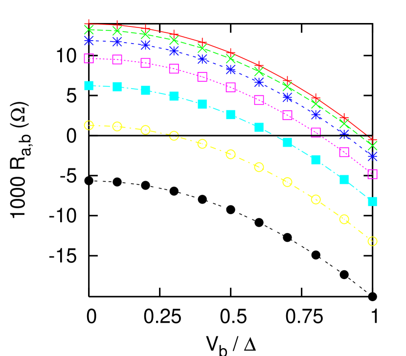
The voltage dependence of the total crossed resistance is shown on Fig. 6 for different values of . We obtain a change of sign from a positive (elastic cotunneling dominated) to a negative (weak localization dominated) crossed resistance as the voltage increases (see Fig. 6). For sufficiently large values of the phase coherence length, we have as discussed above, so that the crossed resistance is negative for all values of the bias voltage.
The perturbative crossed resistance on Fig. 6 tends to a finite value in the limit . The determination of the crossed conductance around is examined in Ref. Melin-Feinberg, for localized interfaces with arbitrary interface transparencies. The non perturbative crossed conductance tends to zero for , but the cross-over occurs within an energy window that becomes very small for tunnel interfaces. A crossed current related to out-of-equilibrium quasiparticle populations (not described here) is expected for .
As it is visible on Fig. 6, the characteristic voltage scale in the bias voltage dependence of the crossed resistance is the superconducting gap, not the normal state superconductor Thouless energy obtained in experiments. At the present stage, we do not find a plausible explanation of this experimental observation.
III.6 Magnetic field dependence
The experimental crossed signal is suppressed by a magnetic field parallel to the layers Russo . The theoretical weak localization crossed signal is also suppressed by a magnetic field because the corresponding diagram dephases in an applied magnetic field. The cross-over magnetic field for the suppression of the weak localization crossed conductance corresponds to one superconducting flux quantum enclosed in the area of the diagram, compatible with experiments Russo . However, in experiments, the crossed resistance is suppressed by a magnetic field in the entire voltage range. The present model does not explain the dephasing of the elastic cotunneling contribution.
IV Conclusions
We have calculated the weak localization contribution to non local transport in NISIN trilayers with extended interfaces and a sufficient phase coherence length in the normal electrodes. We find a change of sign in the crossed resistance between elastic cotunneling at low voltages and weak localization at higher voltages. The weak localization contribution can dominate for all voltages if the phase coherence length is large enough. The weak localization crossed conductance dephases in an applied magnetic field, but not the elastic cotunneling contribution. The appearance of a voltage scale related to the superconductor Thouless energy is left as an important open question.
The author thanks H. Courtois, A. Morpurgo, and S. Russo for many useful suggestions and comments. Special thanks to D. Feinberg and F. Pistolesi for numerous fruitful discussions.
Appendix A Diffusion probabilities in a normal metal
A.1 Diffusion in the electron-electron channel
We first discuss briefly the normal metal diffuson in the ladder approximation. In the Born approximation, the elastic scattering time in the “11” Green’s function given by
| (20) |
is defined by , with , where is the elastic scattering time at the Fermi level, is the amplitude of the microscopic impurity scattering potential, is the Fermi wave-vector, and the Fermi energy.
Using contour integration, and the identity
| (21) |
with and a function of , we obtain easily
where is the diffusion constant. The Fourier transform of the diffusion probability , given by
| (23) |
where the overline is a disorder averaging and is the bulk hopping integral (see Eq. (1)), is obtained by summing the ladder series, leading to
| (24) |
In this expression has no dimension. Its Fourier transform is such that has no dimension, as expected for a probability.
Appendix B Double NS interface
We provide now explanations to the factor appearing in Eq. (III.4) for quasi-two-dimensional normal electrodes. Because of the conservation of the component of the wave-vector parallel to the interface at each tunneling vertex, and because of the form of the diagram, the diagram on Fig. 4 is evaluated at , where is the projection of (see Appendix A) on a plane parallel to the interfaces. By momentum conservation, a finite value of is transformed in after traversing the entire diagram, so that . The resulting crossed conductance is thus proportional to , where the square is due to the correlated diffusion in the two normal electrodes, and where the diffusion probability is given by Eq. (24). This lead to the factor since the normal metals are quasi-two-dimensional so that , where is the projection of on the normal to the interfaces.
Appendix C Ballistic NISIN trilayer with atomic thickness
We consider in this Appendix a ballistic NISIN trilayer with atomic thickness Buzdin-ato ; Melin-Feinberg-ato in which the three electrodes are two-dimensional, and find a factor , similar to the factor factor discussed previously in the diffusive limit.
The transport formula given by Eq. (II.3) is Fourier transformed, to obtain
| (25) | |||
and the Dyson equations for are also Fourier transformed. The normal metal ballistic Green’s function is given by , where is the kinetic energy with respect to the Fermi level, and where the broadening parameter is given by . Eq. (25) is then expanded diagrammatically. A diagram similar to the one on Fig. 4 leads to a factor .
References
- (1) U.P.R. 5001 du CNRS, Laboratoire conventionné avec l’Université Joseph Fourier
- (2) M.S. Choi, C. Bruder, and D. Loss, Phys. Rev. B 62, 13569 (2000); P. Recher, E. V. Sukhorukov, and D. Loss Phys. Rev. B 63, 165314 (2001)
- (3) G. B. Lesovik, T. Martin, and G. Blatter, Eur. Phys. J. B 24, 287 (2001); N. M. Chtchelkatchev, G. Blatter, G. B. Lesovik, and T. Martin, Phys. Rev. B 66, 161320(R) (2002).
- (4) J. M. Byers and M. E. Flatté, Phys. Rev. Lett. 74, 306 (1995).
- (5) G. Deutscher and D. Feinberg, App. Phys. Lett. 76, 487 (2000);
- (6) P. Samuelson, E. V. Sukhorukov, and M. Büttiker, Phys. Rev. Lett. 91, 157002 (2003).
- (7) E. Prada and F. Sols, Eur. Phys. J. B 40, 379 (2004).
- (8) C. J. Lambert, J. Koltai, and J. Cserti, Towards the Controllable Quantum States (Mesoscopic Superconductivity and Spintronics, 119, Eds H. Takayanagi and J. Nitta, World Scientific (2003).
- (9) D. Beckmann, H.B. Weber, and H. v. Löhneysen, Phys. Rev. Lett. 93, 197003 (2004).
- (10) S. Russo, M. Kroug, T.M. Klapwijk, and A.F. Morpugo, Phys. Rev. Lett. 95, 027002 (2005).
- (11) R. Mélin and S. Peysson, Phys. Rev. B 68, 174515 (2003); R. Mélin, Phys. Rev. B 72, 134508 (2005).
- (12) A.F. Andreev, Sov. Phys. JETP 19, 1228 (1964).
- (13) C.J. Lambert and R. Raimondi, J. Phys.: Condens. Matter 10, 901 (1998).
- (14) F.J. Jedema et al., Phys. Rev. B 60, 16549 (1999).
- (15) G. Falci, D. Feinberg, and F.W.J. Hekking, Europhysics Letters 54, 255 (2001).
- (16) The crossed resistance , measured experimentally in Ref. Russo , has a sign opposite to the crossed conductance.
- (17) D. Feinberg, Eur. Phys. J. B 36, 419 (2003).
- (18) N. M. Chtchelkatchev and I. S. Burmistrov, Phys. Rev. B 68, 140501 (2003).
- (19) R. Mélin and D. Feinberg, Eur. Phys. J. B 26, 101 (2002).
- (20) R. Mélin and D. Feinberg, Phys. Rev. B 70, 174509 (2004).
- (21) A. A. Abrikosov, L. P. Gorkov, and I. E. Dzyaloshinski, Methods of Quantum Field Theory in Statistical Physics (Dover, New York, 1963).
- (22) C. Caroli, R. Combescot, P. Nozi res, et D. Saint-James, J. Phys. C 4, 916 (1971); 5, 21 (1972).
- (23) A. Martin-Rodero, F. J. Garcia-Vidal, and A. Levy Yeyati, Phys. Rev. Lett. 72, 554 (1994).
- (24) A. Levy Yeyati, A. Martin-Rodero, and F. J. Garcia-Vidal, Phys. Rev. B 51, 3743 (1995).
- (25) A. Levy Yeyati, A. Martin-Rodero, and J. C. Cuevas, J. Phys.: Condens. Matter 8, 449 (1996).
- (26) J.C. Cuevas, A. Martín-Rodero and A. Levy Yeyati, Phys. Rev. B 54, 7366 (1996), and references therein.
- (27) R. A. Smith and V. Ambegaokar, Phys. Rev. B 45, 2463 (1992).
- (28) F.W.J. Hekking and Yu. V. Nazarov, Phys. Rev. Lett. 71, 1625 (1993).
- (29) C. Beenakker, Rev. Mod. Phys. 69, 731 (1997).
- (30) A. Buzdin and M. Daumens, Europhys. Lett. 64, 510 (2003).
- (31) R. Mélin and D. Feinberg, Europhys. Lett. 65, 96 (2004)