Time-Resolved Spin Torque Switching and Enhanced Damping in Py/Cu/Py Spin-Valve Nanopillars
Abstract
We report time-resolved measurements of current-induced reversal of a free magnetic layer in Py/Cu/Py elliptical nanopillars at temperatures = 4.2 K to 160 K. Comparison of the data to Landau-Lifshitz-Gilbert macrospin simulations of the free layer switching yields numerical values for the spin torque and the Gilbert damping parameters as functions of . The damping is strongly -dependent, which we attribute to the antiferromagnetic pinning behavior of a thin permalloy oxide layer around the perimeter of the free layer. This adventitious antiferromagnetic pinning layer can have a major impact on spin torque phenomena.
pacs:
85.75.-d, 75.75.+a, 81.65.MqExperiments Katine et al. (2000); Urazhdin et al. (2003); Kiselev et al. (2003); Grollier et al. (2000) have shown that a spin-polarized current passed through a nanomagnet can excite a dynamic response as the result of a spin torque applied by the conduction electrons Slonczewski (1996); Berger (1996). The potential for technological impact of this spin transfer (ST) effect has inspired research in DC current-induced microwave oscillations Kiselev et al. (2003); Rippard et al. (2005) and hysteretic switching Katine et al. (2000); Urazhdin et al. (2003); Grollier et al. (2000) in current perpendicular to the plane (CPP) nanopillars and nanoconstrictions. Typically, ST switching data is obtained through the use of slow current ramp rates (1 mA/s), but fast pulses (1010 mA/s) access the regime where thermal activation of the moment over a current-dependent barrier Li and Zhang (2004); Krivorotov et al. (2004) does not play a major role in the switching process. This spin torque-driven regime Koch et al. (2004) is advantageous for the quantitative examination of the spin torque parameters due to the computational accessibility of numerically integrating the Landau-Lifshitz-Gilbert (LLG) equation for short durations.
Here we report time-resolved measurements of the spin torque-driven switching event in Cu 100/Py 20/Cu 6/Py 2/Cu 2/Pt 30 (in nm, Py = Ni81Fe19) CPP spin-valve nanopillar structures at bath temperatures = 4.2 K to 160 K. We compare our experimental results with LLG simulations in the macrospin approximation and find good agreement between simulation and measurement. This both confirms the applicability of the macrospin approximation in the spin torque-driven regime and facilitates the quantitative determination of -dependent spin torque and magnetic damping parameters. At higher we find that the strength of the spin torque exerted per unit current is in reasonable numerical accord with recent model calculations, and that the damping parameter for the nanomagnet excitations is both anomalously high, as suggested by previous pulsed current measurements Braganca et al. (2005), and -dependent. The strong variation of , in conjunction with anomalous behavior of the nanomagnet switching fields () in some devices, points to the presence of an adventitious antiferromagnetic oxide layer around the perimeter of the nanomagnet that has a major effect on the nanomagnet dynamics driven by a spin torque.
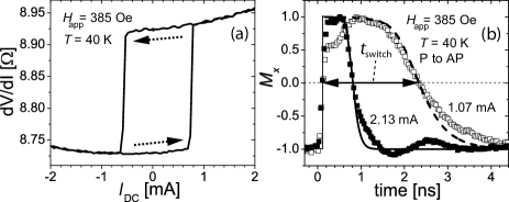
The nanopillar devices employed in this study were fabricated using a process described elsewhere Emley et al. (2004). A slow ramp rate ST scan is shown in Fig. 1(a) for sample 1, a 60190 nm ellipse. In Fig. 1(b) we show parallel (P) to anti-parallel (AP) switching events for sample 1, averaged over 10,000 switches, taken at pulsed current amplitudes = 1.07 mA and 2.13 mA at = 40 K as open and solid squares, respectively. The measured signal is a time-resolved voltage drop from the giant magnetoresistance (GMR) of the sample as the free layer switches from P to AP orientation, where (AP)(P) and is the 4-point device resistance. The data have been normalized to (minimum resistance / maximum resistance) for simple comparison with simulated switching events, described below, which are shown as solid and dashed lines. The abrupt (200 ps) jump from = -1 to 1 at time = 0 is not a switching event but is simply the rising edge of the current pulse. The more gradual transition between P ( = 1) and AP (return to = -1) is the envelope coming from averaging over thousands of individual switching events, each of which follows a trajectory determined by initial conditions that are randomized by the stochastic thermal fluctuations of the free layer. We define the switching time as the time elapsed between 50% of the signal rise and 50% of the signal drop as indicated in Fig. 1(b) jit .
To obtain a quantitative understanding of the ST switching, we have simulated the nanomagnet dynamics by numerical integration of the LLG equation in the macrospin approximation with the inclusion of a Slonczewski-type spin torque term.
Here is the gyromagnetic ratio, is the unit directional vector of the free layer macrospin, is the spin polarization axis, is the in-plane angle between them, is the spin torque function, is the free layer magnetization, as measured separately for a continuous 2 nm Py film in a Cu/Py/Cu trilayer that was exposed to the same heat treatments as the nanopillars, is the nanomagnet thickness, is its lateral area with dimensions and that are estimated by OOMMF micromagnetic simulations Donahue and Porter (1999) (see below), and is the sum of external , in-plane anisotropy , and out-of-plane anisotropy fields. is the sum of the magnetostatic dipole field from the fixed layer and the applied field from the electromagnet, which is adjusted to compensate for so .
The initial conditions of the simulation were set by = + + , where = 0∘ for P to AP and 180∘ for AP to P switching and represents any systematic angular misalignment between free and fixed layer moments due to the setup and was generally set to 0. The random angle is treated as a Gaussian with a standard deviation where is the uniaxial anisotropy energy. (4.2 K), , and are estimated from = 0, 2D OOMMF simulations of Py elliptical disks having and values similar to those measured at 4.2 K. The lateral area is estimated to 12% uncertainty with this method, nearly a factor of 2 better than the inherent shape variation among otherwise identical elliptical patterns due to lithographic fluctuations. Ohmic heating effects during the current pulse are taken into account by locally raising the temperature of the device to Krivorotov et al. (2004). A Langevin field accounts for thermal fluctuations during the dynamic trajectory, fluctuating randomly in 3-dimensions with a standard deviation where = 1 ps is the time step Li and Zhang (2004); Koch et al. (2004); Russek et al. (2005). Gilbert damping is assigned an angular dependence , where = 0.33 for Py/Cu/Py nanopillars Tserkovnyak et al. (2003), but the addition of this angle-dependent damping term had only a small effect on the simulation results.
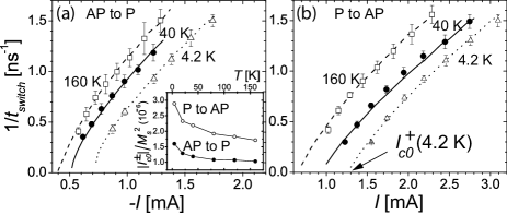
The spin torque function is approximated by where and are phenomenological parameters Braganca et al. (2005); Slonczewski (2002); Xiao et al. (2004). In our simulations we use , , and as -dependent fitting parameters to match the simulated with the measured values of 1/ versus for each , where we allow to be different for the two switching directions. In Fig. 1(b) we plot the average of 2000 simulated P to AP switching events at = 40 K alongside the normalized data for sample 1 with the best fit simulation yielding = 0.5, = 0.11, and = 0.048. Since the current step in the simulation turns on instantaneously, an average pulse half rise time of 112 ps, measured from data such as those in Fig. 1(b), has been added to all simulated . We plot measured 1/ versus for AP to P and P to AP switching at = 160 K, 40 K, and 4.2 K for sample 2, an 80180 nm ellipse, together with best fit simulations, all of which are averages over 2000 events, in Fig. 2(a) and 2(b), respectively. Simulations out to long switching times (1/ ns-1) allow for good estimates of the 1/ intercepts , which are the critical currents (+ = P to AP) defining the onset of spin torque-driven switching. These should depend on the spin torque and damping parameters as Koch et al. (2004). A striking result from these measurements is the strong -dependence of (Fig. 2(a) inset), which varies by more than 60% over the entire range, where the upturns at low indicate a strong dependence of damping, spin torque, or both.
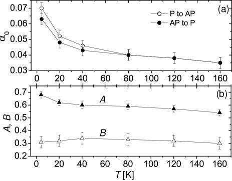
In Fig. 3 the best fit values for , , and (assuming = 0∘) are plotted as functions of for sample 2. Uncertainties in the fit parameters, = 0.0035, = 0.025, and = 0.045, are found through an exploration of parameter space about the best fit values. Accounting for these -dependences, the theoretical prediction of agrees with the measurement to within 10% over the entire range of . All four devices that were extensively studied show an amplitude and -dependence of very similar to that of Fig. 3(a); a gradual but significant increase with decreasing below 160 K, above which the devices are thermally unstable, followed by a stronger increase starting below 60 K - 40 K where the best fit values of also suggest differences between the two switching directions. For 60 K, the trends in the -dependence of the spin torque parameters and vary from sample to sample, but for 60 K both consistently show a very mild dependence on as illustrated in Fig. 3(b). For the four samples studied in detail we found that at 40 K ranged from 0.5 to 0.68 and varied from 0.11 to 0.35. In general we also found that would decrease by 10 or 20% in going from 40 K to 160 K while would typically vary by 10% or less. These values of and and the variation with 60 K can be compared with the results of a two-channel model Valet and Fert (1993) with which the measured GMR parameters, and , can be used to predict the spin torque parameters Garcia . This model predicts = 0.52, = 0.36 at 40 K, with decreasing to 0.47 at 160 K and remaining essentially constant. This is in reasonable accord with the data, given the experimental uncertainties in nanomagnet size and alignment.
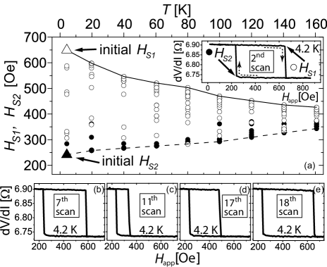
We attribute the significant -dependence of to the presence of a weak antiferromagnetic (AF) layer on the sidewalls of the nanopillar. Although no such AF layer was deliberately deposited, the exposure of the nanopillars to air after ion mill definition undoubtedly oxidized the sidewalls, thus allowing for AF Py oxide to form and weakly exchange bias the ferromagnetic layers. An example of direct evidence for this adventitious exchange biasing is shown in Fig. 4, where switching fields and , defined in the inset, from 20 field scans at each , are plotted from 4.2 K to 160 K for sample 3, an 80180 nm ellipse, a previously unmeasured device cooled in . Note that varies more rapidly with than , which is indicative of an exchange bias that strengthens with decreasing (particularly rapidly below 40 K) and promotes AP alignment, i.e. a bias set by the dipole field from the fixed layer. Another key point illustrated in Fig. 4 is the large variation that develops in , and to a lesser extent in , upon multiple minor loop scans after the device is cooled to low . Initially, the device switches repeatedly with nearly the same switching fields, but after six or seven magnetic reversals the switching fields begin to fluctuate greatly from reversal to reversal, indicating stochastic variations in the net strength of the oxide pinning field. While the effects of the random pinning field are particularly pronounced at 4.2 K they are observed up to 160 K, indicating that some degree of magnetic ordering within the AF persists over this entire range and also that each reversal of the free layer nanomagnet has an irreversible perturbing effect on the magnetic structure of the AF oxide. It is important to note that the slow ramp rate current-driven switching events at low for these devices show good reproducibility, with little variation from one sweep to another, as should be the case because ST switching currents are less sensitive to field variations than are the switching fields. The strength of this low AF exchange biasing varies from device to device, with some samples showing no random variations in . We do not believe that fluctuations of this sort have affected any previously-published conclusions from our group. Nevertheless, the fluctuations visible in some samples indicate clearly the presence of an AF layer that should influence the properties of all nanopillar ST devices.
Exchange biasing in AF/Py films has been demonstrated to dissipate dynamic magnetic energy through a two-magnon scattering process arising from local variations in the interfacial exchange coupling McMichael et al. (1998); Rezende et al. (2001); Weber et al. (2005). Over the course of the pulsed measurements, the free layer is switched hundreds of millions of times, which the data indicate should result in the AF layer being on average magnetically ordered but with a finer, more randomized local magnetic structure that leads to strong damping. The rapid increase in damping, observed over the same low range where both the unidirectional AF pinning field and the critical currents also increase rapidly, is attributed to an increasing portion of the AF oxide layer becoming blocked, thereby simultaneously increasing the amount of interfacial exchange coupling variation seen by the free layer nanomagnet as it moves in its dynamic switching trajectory, consistent with the two-magnon model. The process of inducing randomization in the AF by the nanomagnet reversal itself may also lead to enhanced damping. The unidirectional pinning field is present over the entire range, with diminishing amplitude with increasing . As the AF grains become unblocked, an additional damping mechanism becomes possible if these grains can undergo reversal on the same time scale that the free layer traces out its dynamic switching trajectory, which can result in domain drag or the “slow relaxer” dissipation process McMichael et al. (2000). This effect could make a significant contribution to the greater than intrinsic damping that persists to higher .
Most ST device fabrication processes currently employed expose the sides of the free layer nanomagnet to some level of an oxidizing ambient at some point, either during or after processing and to our knowledge there have been no reports of actively protecting the sidewalls from oxidation. We suggest that the native AF oxide layer that forms can have substantial, previously under-appreciated consequences for the ST behavior, leading to a substantially enhanced damping parameter which directly increases the critical currents for switching. The presence of this AF perimeter layer may also alter the boundary conditions that should be employed in micromagnetic modeling of the free layer nanomagnet behavior and affect the dynamical modes of ST-driven precession. We are currently investigating whether this AF perimeter layer can account, at least in part, for the narrower than predicted ST-induced microwave oscillator linewidths that have been observed in similar nanomagnets at low Sankey et al. .
In summary, we have performed time-resolved measurements of the spin torque-driven switching of a Py nanomagnet at = 4.2 K to 160 K. LLG macrospin simulations are in close quantitative agreement with the ST switching events, yielding values of the parameterized spin torque function and the damping parameter. We find to be high, 0.03, and strongly -dependent, which we attribute to the AF pinning behavior of a thin Py oxide layer on the sidewall of the nanomagnet. The values of and are in fair numerical agreement with the spin torque calculated from the two-channel model using the measured magnetoresistance values of the nanopillar spin-valve. There is, however, considerable device-to-device variation in the spin torque asymmetry parameter , which we tentatively attribute to the variable nature of the AF perimeter layer. The presence of an AF oxide layer can have a major effect on the nanomagnet dynamics. Controlling this layer will be important in optimizing spin torque-driven behavior.
This research was supported by ARO - DAAD19-01-1-0541, and by NSF through the NSEC support of the Cornell Center for Nanoscale Systems. Additional support was provided by NSF through use of the facilities of the Cornell Nanoscale Facility - NNIN and the facilities of the Cornell MRSEC.
References
- Katine et al. (2000) J. A. Katine et al., Phys. Rev. Lett. 84, 3149 (2000).
- Urazhdin et al. (2003) S. Urazhdin et al., Phys. Rev. Lett. 91, 146803 (2003).
- Kiselev et al. (2003) S. I. Kiselev et al., Nature (London) 425, 380 (2003).
- Grollier et al. (2000) J. Grollier et al., Appl. Phys. Lett. 78, 3663 (2000).
- Slonczewski (1996) J. C. Slonczewski, J. Magn. Magn. Mater. 159, L1 (1996).
- Berger (1996) L. Berger, Phys. Rev. B 54, 9353 (1996).
- Rippard et al. (2005) W. H. Rippard et al., Phys. Rev. Lett. 95, 067203 (2005).
- Li and Zhang (2004) Z. Li and S. Zhang, Phys. Rev. B 69, 134416 (2004).
- Krivorotov et al. (2004) I. N. Krivorotov et al., Phys. Rev. Lett. 93, 166603 (2004).
- Koch et al. (2004) R. H. Koch et al., Phys. Rev. Lett. 92, 088302 (2004).
- Braganca et al. (2005) P. M. Braganca et al., Appl. Phys. Lett. 87, 112507 (2005).
- Emley et al. (2004) N. C. Emley et al., Appl. Phys. Lett. 84, 4257 (2004).
- (13) Jitter noise in the triggering of the oscilloscope prevents the complete removal of distortions in the pulse shape coming from the pulser and amplifier, giving a slowly oscillating background and a shoulder in the current step. These introduce a maximum error of only 7% in the measurements of and are not significant. AP to P switching data (not shown) are very similar in both time and scales.
- Donahue and Porter (1999) M. J. Donahue and D. G. Porter, Tech. Rep., NIST, Gaithersburg, MD (1999).
- Russek et al. (2005) S. E. Russek et al., Phys. Rev. B 71, 104425 (2005).
- Tserkovnyak et al. (2003) Y. Tserkovnyak et al., Phys. Rev. B 67, 140404 (2003).
- Slonczewski (2002) J. C. Slonczewski, J. Magn. Magn. Mater. 247, 324 (2002).
- Xiao et al. (2004) J. Xiao et al., Phys. Rev. B 70, 172405 (2004).
- Valet and Fert (1993) T. Valet and A. Fert, Phys. Rev. B 48, 7099 (1993).
- (20) A. G. F. Garcia, unpublished.
- McMichael et al. (1998) R. D. McMichael et al., J. Appl. Phys. 83, 7037 (1998).
- Rezende et al. (2001) S. M. Rezende et al., Phys. Rev. B 63, 214418 (2001).
- Weber et al. (2005) M. C. Weber et al., J. Appl. Phys. 97, 10A701 (2005).
- McMichael et al. (2000) R. D. McMichael et al., J. Appl. Phys. 87, 6406 (2000).
- (25) J. C. Sankey et al., eprint cond-mat/0505733.