Lateral diffusive spin transport in layered structures
Abstract
A one dimensional theory of lateral spin-polarized transport is derived from the two dimensional flow in the vertical cross section of a stack of ferromagnetic and paramagnetic layers. This takes into account the influence of the lead on the lateral current underneath, in contrast to the conventional 1D modeling by the collinear configuration of lead/channel/lead. Our theory is convenient and appropriate for the current in plane configuration of an all-metallic spintronics structure as well as for the planar structure of a semiconductor with ferromagnetic contacts. For both systems we predict the optimal contact width for maximal magnetoresistance and propose an electrical measurement of the spin diffusion length for a wide range of materials.
pacs:
72.25.Dc, 72.25.Mk, 85.75.-dSpintronics promises an increase in the logical expressibility of electronic circuits and the integration of non-volatile magnetic memory Wolf_Science00 ; Zutic_RMP04 . A quantitative and yet simple theory of spin transport is essential for interpreting experimental results and designing practical lateral devices which are imperative in large scale integrations. The most popular analytical approach to spin transport extends drift-diffusion equations to include the spin degree of freedom VanSon_PRL87 ; Valet_PRB93 ; Hershfield_PRB97 ; Yu_Flatte_long_PRB02 . One-dimensional equations of this kind have successfully explained the current-perpendicular-to-the-plane giant magnetoresistance Valet_PRB93 and the spin injection from a ferromagnetic metal into a semiconductor in a vertical geometry VanSon_PRL87 ; Schmidt_PRB00 ; Rashba_PRB00 ; Yu_Flatte_long_PRB02 ; Albrecht_PRB03 . Theories of spin transport for current in plane focus on boundary scattering to explain the magnetoresistive effect in ultrathin layered system Levy_SSP94 ; hershfield_cip . However, many of the experiments involving non-magnetic metals Johnson_Science93 ; Jedema_Nature01 or semiconductors Stephens_PRL04 ; Crooker_Science05 are performed in the planar geometry where the thickness of the layers exceeds the mean free path. For these systems, application of either of the existing 1D models is a rough approximation, unable to account for some observed features whose interpretation required a numerical 3D treatment Hamrle_PRB05 . The role of the contact width in lengthening the effective path between two leads versus the spin diffusion length was mentioned Fert_PRB01 . The effect of leakage from two-dimensional electron gas into the ferromagnetic gate of finite lateral size on the spin currents in the channel has been investigated McGuire_PRB04 . What remains lacking is a simple theory in which the spin injection from contacts of finite width is normal to the spin current in the plane of the conduction channel.
In this paper, starting from a study of the two dimensional current flow in the vertical cross section of the planar system, we derive an analytical 1D theory of spin transport in lateral structures. The analysis takes into account the lateral extent of the interface between ferromagnetic (FM) and normal (N) materials. We obtain a transparent physical picture and derive useful analytical formulas. The most important result obtained is the dependence of the magneto-resistance (MR) on the contact width. The knowledge of this aspect of lateral spin-valve physics is essential to the design of structures with high MR. In addition, our analysis suggests a technique to obtain the spin diffusion length of a paramagnetic material by a simple set of electrical measurements. For compounds, such as silicon, which are inaccessible to optical characterization of spin polarization Stephens_PRL04 ; Crooker_Science05 , development of the electrical method is of great importance.
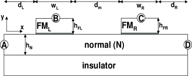
Fig. 1 depicts a typical planar system, homogeneous in the direction. A model of one dimensional current flow from lead B via the normal region to lead C cannot describe the flow under the leads because of the simultaneous in-plane flow and the injection or extraction from above. Hence, we must first consider the two-dimensional transport governed by the spin diffusion equation:
| (1) |
where is the spin dependent electrochemical potential with = denoting the spin species. The characteristic distance of spin flip is , where is the spin-flip time and is the diffusion constant of the spin component . The measurable spin diffusion length , on whose scale the splitting of changes, is given by . These equations hold for ferromagnetic and normal metals Hershfield_PRB97 and also hold for non-degenerate semiconductors with the additional condition of a small electric field Yu_Flatte_long_PRB02 . We neglect interfacial spin scattering and use Ohm’s law across the interfaces. Since the current is driven by the gradient of the electrochemical potential, the continuity of the normal component of the spin current across two adjacent layers and provides the boundary conditions,
| (2) |
where and refer to layer conductivity and outward interface normal, respectively, and is the spin-dependent barrier conductance. Although Fig. 1 illustrates only two layers (normal and FM), the equations derived below hold for multilayers.
To reduce the essential features of the two dimensional flow to one dimension, we define the vertical () average of in each layer,
| (3) |
with being the thickness of the layer between its boundaries, . For thin layers, may be replaced by its vertical average . The conditions of validity follow the requirement that the gradient correction along to in Eq. (3) be negligible to ,
| (4) |
with the help of Eqs. (1) and (2). Under these conditions we can derive a set of 1D equations governing the lateral (i.e., in the layer plane) spin transport. Integrating out the dependence in Eq. (1) and using Eq. (2) yields,
| (5) | |||||
This kinetic theory assumes that the relevant length scales exceed the electron mean free path. Thus, the present analysis cannot address the quantum realm of the MR effect in ultrathin layered systems Levy_SSP94 .
We now divide the lateral transport into regions of vertical stacks. Consider a region with a vertical stack of layers. For example, in the region of width covered by the left lead in Fig. 1, , excluding the insulator. Transport in the layers of the stack is governed by coupled members of Eq. (5) which in the matrix form are simply,
| (6) |
with the column vector of elements and the positive definite matrix of elements from Eq. (5). The solution has the form,
| (7) |
where , a column of ones, is an eigenvector of with zero eigenvalue and is an eigenvector with eigenvalue . The connection of the vertical stacks to the outside of the system and to each other is maintained by the boundary conditions. Between stacks they are given by the continuity of and their first derivatives (currents) through each homogeneous layer. At the outermost boundaries (like A and D in Fig. 1) the conditions are prescribed by the external driving terms of the electrochemical potential in the form of either a constant voltage maintained at an electrode or an injection current (including zero) through an interface. Applying currents/voltages to B and C interfaces results in the presence of inhomogenous terms in Eq. (6). These boundary conditions provide a unique set of solutions for the parameters in Eq. (7). This method of solution is a considerable simplification compared to solving the 2D spin diffusion equation for the same planar structure, and yet it includes the influence of the vertical layers on the lateral spin current flow. In the following, we will show the versatility of this simplified approach as well as testing its validity against the 2D solution.
The first illustrative example involves a semiconductor in the normal layer of the structure in Fig. 1. A and D are disconnected from outside while B and C are voltage biased. The spin diffusion length in the normal layer is . We divide the normal channel into sections belonging to 5 vertical stacks as shown in Fig. 1. In the middle section of the channel, the solution is Hershfield_PRB97 ; Yu_Flatte_long_PRB02 ,
| (8) |
where and are constants to be determined by the boundary conditions. The total current flowing between the two leads is per unit length of the structure in the direction. For the two sections outside the footprint defined by the two leads, we introduce the notion of the “open” versus “confined” geometry depending on whether or . In both geometries the pattern of the net charge current occurs only between the leads B and C. This means that the outside sections lack the linear term of Eq. (8). Additionally the “open” geometry includes only an exponentially decaying solution away from the closer lead, and in contrast with the confined geometry, spin polarization extends noticeably outside of the footprint between B and C, thus reducing the spin accumulation densities. In each of the vertical stacks containing a lead, due to vastly different conductivities of the semiconductor and ferromagnetic metal we can decouple the equations for in the N semiconductor and in the FM metal and solve for the eigenvalues of in the former,
| (9) |
where the first of each pair of symbols or takes the upper sign. The electrochemical potential in the FM is practically a constant (), and in the semiconductor layer under the biased lead is
| (10) | |||||
where , , and are constants to be determined by boundary conditions and . Consider the case that spin polarization is robust so that and are comparable. If , then and . The -mode is limited by the spin diffusion constant, and it corresponds to spin accumulation ( in this case). If , then both eigenvalues are nearly independent of , and neither of the eigenvectors is a pure spin mode : the inhomogeneity of injection dominates the spatial dependence.
To illustrate the effect of the contact width on MR, we use the experimentally verified barrier parameters of a Fe/GaAs system at 300K Hanbicki_APL02 ; Hanbicki_APL03 . The tunneling conductances are of the order of -cm-2 with the ratio of spin-up to spin-down conductance . The N channel doping is cm-3 and the spin relaxation time is ps Optical_Orientation which corresponds to 1m. The thickness of the N channel is nm, and the inner channel length is nm.
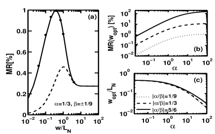
The MR effect is defined as with () being the total current when the FM contacts are magnetized in parallel (antiparallel) directions. The calculated MR is shown in Fig. 2(a) as a function of the contact width, where for simplicity we have used . In the confined geometry, =, the effective 1D method (solid line) is compared with the results of 2D numerical calculation (dots), showing excellent agreement. We note the deleterious effect of the open geometry (dashed line) compared with the confined geometry (solid line) because of the weaker spin accumulation in the semiconductor channel which produces the MR effect Dery_cm .
Note the existence of the optimal contact width for the maximum MR effect which arises out of the balance between spin injection and spin relaxation in the channel. The spin accumulation in the normal conduction channel is built up from injection along the width of the ferromagnetic contact. When the width is small, inadequate build-up results in small spin injection and spin accumulation as a percentage of the equilibrium carrier density. Consequently the MR effect is small. However, when the contact width is too large, its resistance becomes very small, the MR effect in the N channel is again negligible as in the conventional one-dimensional model Rashba_PRB00 . Finally, when the contact width exceeds the spin diffusion length , the build-up from vertical injection along the width of the contact beyond becomes ineffective, the spin injection and the MR effect approach asymptotic values. The difference between the open and confined structures is removed, as can be seen from the merging of the solid and dashed lines in Fig. 2(a). The magnitude of MR at the optimal contact width depends also on the spin selectivity of the barriers, in Eq. (9), as illustrated in Fig. 2(b). Fig. 2(c) shows a much weaker dependence on the spin selectivity of the optimal contact width in units of the spin diffusion length (). The ratio depends only on as defined in Eq. (9). For , . For , the optimal contact width is approximately 6/5 or 3/8 for the open or confined geometry, respectively. These results enable the extraction of the spin diffusion length of a test material by measuring the MR of several structures with different contact widths from the same growth.
To demonstrate the use of our method for the all-metallic system, we turn to a second example. In the planar structure of Fig. 1, a constant current is injected from region A into a 10 nm paramagnetic metal layer. The structural parameters in terms of the spin diffusion length of the N layer are . The FM layers B and C are of the same thickness and serve as floating contacts. We use the Al/Co system parameters at 300K where ratio of spin-up to spin-down conductance is Vouille_PRB99 and their sum is . The normal layer intrinsic parameters are , m. In the Co layers the majority channel conductivity and spin diffusion lengths are, respectively, and 12 nm. The respective values of the Co minority channel are and 20 nm. For ease of toggling between and configurations we use a width ratio of 2 between left and right Co regions. For the FM/N regions the solutions are given by Eq. (7). In the middle N channel the solution of is given by Eq. (8) while at the outer channels the form of lacks the diverging exponential.
For each magnetic configuration ( or ) we calculate the voltage drop with the electrochemical potentials averaged along each Co layer. The MR is defined as . Fig. 3(a) shows the MR effect. It peaks at the right contact width of . The optimal contact width mostly on , insensitive to varying the spin selectivity, the middle N channel length, or the outer N channel lengths (not shown). Fig. 3(b) and (c) show, respectively, the current densities in the normal layer for parallel and antiparallel magnetic configuration at the optimal contact width. The solid (dashed) lines depict spin up and spin down current components along the x direction. Despite the small MR effect, its observation is well within existing experimental abilities. Thus a similar analysis to the previous FM/SC example leads to an electrical method to measure the spin diffusion length of the normal material. However, the extraction of requires that it greatly exceeds the FM spin diffusion length.

In summary, we have presented an effective 1D theory which describes spin dependent transport beneath and between ferromagnetic contacts in the lateral geometry. Under the conditions of thin layers and non-ohmic interfaces, the derived set of coupled linear equations governing the lateral diffusive spin currents is almost as accurate as the 2D spin diffusion equation but much simpler to use. This method retains the important role of the contact width, predicting an optimal contact width for the maximal magneto-resistive effect in the lateral spin-valve. We have also quantified the effect of “open” channels, where spins can diffuse away from the active region underneath the FM contacts, in contrast with the “confined” structures, where the spin accumulation is kept between the two contacts. Our results provide crucial guidelines for design of lateral spin-valve type devices. They also yield a method of extracting the spin-diffusion length in an all-electrical measurement. At room temperature where the spin diffusion length lies in the sub-micron region, this method does not have the difficulty of wavelength resolution in the optical techniques.
This work is supported by NSF DMR-0325599.
References
- (1) S. A. Wolf, D. D. Awschalom, R. A. Buhrman, J. M. Daughton, S. von Molnar, M. L. Roukes, A. Y. Chtchelkanova, and D. M. Treger, Science 294, 1488 (2001).
- (2) I. Z̆utić, J. Fabian, and S. D. Sarma, Rev. Mod. Phys. 76, 323 (2004).
- (3) P. C. van Son, H. van Kempen, and P. Wyder, Phys. Rev. Lett 58, 2271 (1987).
- (4) T. Valet and A. Fert, Phys. Rev. B 48, 7099 (1993).
- (5) S. Hershfield and H. L. Zhao, Phys. Rev. B 56, 3296 (1997).
- (6) Z. G. Yu and M. E. Flatt e, Phys. Rev. B 66, 235302 (2002)
- (7) G. Schmidt, D. Ferrand, L. W. Molenkamp, A. T. Filip, and B. J. van Wees, Phys. Rev. B 62, R4790 (2000).
- (8) E. I. Rashba, Phys. Rev. B 62, R16267 (2000).
- (9) J. D. Albrecht and D. L. Smith, Phys. Rev. B 68, 035340 (2003).
- (10) P. M. Levy, Solid State Physics (Academic, New York, 1994), vol. 47, p. 367.
- (11) K. Majumdar, J. Chen, and S. Hershfield, Phys. Rev. B 57, 2950 (1998).
- (12) M. Johnson, Science 260, 320 (1993).
- (13) F. J. Jedema, A. T. Filip, and B. J. van Wees, Nature 410, 345 (2001).
- (14) J. Stephens, J. Berezovsky, J. P. McGuire, L. J. Sham, A. C. Gossard, and D. D. Awschalom, Phys. Rev. Lett. 93, 097602 (2004).
- (15) S. A. Crooker, M. Furis, X. Lou, C. Adelmann, D. L. Smith, C. J. Palmstrom, and P. A. Crowell, Science 309, 2191 (2005).
- (16) J. Hamrle, T. Kimura, Y. Otani, K. Tsukagoshi, and Y. Aoyagi, Phys. Rev. B 71, 094402 (2005).
- (17) A. Fert and H. Jaffrès, Phys. Rev. B 64, 184420 (2001).
- (18) J. P. McGuire, C. Ciuti, and L. J. Sham, Phys. Rev. B 69, 115339 (2004).
- (19) A. T. Hanbicki, B. T. Jonker, G. Itskos, G. Kioseoglou, and A. Petrou, Appl. Phys. Lett. 80, 1240 (2002).
- (20) A. T. Hanbicki, O. M. J. van t Erve, R. Magno, G. Kioseoglou, C. H. Li, B. T. Jonker, G. Itskos, R. Mallory, M. Yasar, and A. Petrou, Appl. Phys. Lett. 82, 4092 (2003).
- (21) Optical Orientation, edited by F. Meier and B. P. Zakharchenya (Nort-Holland, New York, 1984).
- (22) H. Dery, Ł. Cywiński, and L. J. Sham, cond-mat 0507378, (2005)
- (23) C. Vouille, A. Barthélémy, F. Elokan Mpondo, A. Fert,P. A. Schroeder, S. Y. Hsu,A. Reilly, and R. Loloee, Phys. Rev. B 60, 6710 (1999).