Mobility in semiconducting carbon nanotubes at finite carrier density
Abstract
Carbon nanotube field-effect transistors operate over a wide range of electron or hole density, controlled by the gate voltage. Here we calculate the mobility in semiconducting nanotubes as a function of carrier density and electric field, for different tube diameters and temperature. The low-field mobility is a non-monotonic function of carrier density, and varies by as much as a factor of 4 at room temperature. At low density, with increasing field the drift velocity reaches a maximum and then exhibits negative differential mobility, due to the non-parabolicity of the bandstructure. At a critical density 0.35-0.5 electrons/nm, the drift velocity saturates at around one third of the Fermi velocity. Above , the velocity increases with field strength with no apparent saturation.
Carbon nanotubes have enabled new nano-electronic devices such as quasi-one-dimensional field-effect transistors (CN-FET) Avouris and electro-optical devices Misewich ; Marcus2 . Ballistic devices have generated excitement as the ideal limit of transistor performance Javey1 . Yet diffusive devices remain important Marcus2 ; Snow ; Grunner due to the very high mobility even at room temperature Durkop . Much effort has gone into determining their transport properties experimentally Yao ; Javey ; Park ; Zhou ; ChenF and theoretically Pennington ; Perebeinos3 ; Guo ; Verma .
Conventional transistors operate by control of carrier density, i.e. band filling via an external gate electrode and its capacitive coupling to the conduction channel. Yet while carrier density is a crucial variable in device operation, relatively little is known about how the mobility in nanotube transistors varies with carrier density, especially at high fields. Only recently have systematic studies of the dependence on gate voltage been reported Zhou ; ChenF .
Here we calculate the mobility in carbon nanotubes as a function of charge carrier density. We find that the mobility depends sensitively on carrier density. Specifically, at low field and low temperature, the mobility initially increases with carrier density, because the phase space for scattering disclaimer is reduced by band filling. The mobility then decreases abruptly as the band filling reaches the second band, because a new channel for scattering opens up. The low-field mobility can be expressed as the product of scattering time and hinverse effective mass, where the effective mass is nearly independent of temperature, and increases smoothly with band filling. Our results quantify a recent analysis of low-field mobility Zhou .
At high fields, we find negative differential mobility (NDM) at low density, decreasing and disappearing with increasing density. Surprisingly, this NDM appears to be unrelated to the occupation of the second band, but can be ascribed to the nonparabolicity of the first band. The minimum differential mobility, i.e. maximum magnitude of the NDM, increases with diameter and decreases with temperature, with a systematically larger value in tubes with mod than in those with mod. This is due to the stronger band nonparabolicity in the former.
Our calculations use a tight-binding description for the electronic structure Saito . The phonons are described using a model similar to that of Aizawa et al. Aizawa . We model the electron-phonon interaction by the Su-Schrieffer-Heeger model Su , with matrix element dependent on the change of the nearest neighbor C-C distance (), where eV. We take the electron-phonon coupling constant to be eV/Å Perebeinos2 .
We solve the steady-state multi-band Boltzmann equation in the presence of an electric field, to determine the electron distribution function :
| (1) | |||||
where is an electron-phonon scattering rate Perebeinos3 . The indices k and q label both the continuous wave vector along the tube axis and the band index. Using the non-equilibrium distribution function from Eq. (1), we calculate the drift velocity and the mobility according to:
| (2) |
where is the band velocity and is the band filling factor (electrons/carbon).
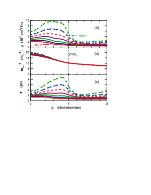
The low-field electron mobility is shown in Fig. 1a for a (19,0) tube. (The hole mobility is identical, due to the electron-hole symmetry in our model.) The mobility has a complex and highly non-monotonic dependence on density at low temperature, and decreases at higher temperature due to phonon scattering.
To understand the low-field mobility, we use the classical relationship to decompose the mobility into a product of two terms: the scattering time and the averaged inverse effective mass . The natural definition of and resulting definition of are disclaimer3 :
| (3) |
The effective mass contribution to the low-field mobility is shown in Fig. 1b - it is virtually independent of temperature and it is a monotonically decreasing function of the electron density . In contrast, the scattering time contribution in Fig. 1c has a strong dependence on both temperature and charge density. The charge scale is determined primarily by the density at which the first band is filled up to the energy of the bottom of the second band (at K). The scattering time drops sharply around , reaching a minimum before rising again.
At low field, is given essentially by the Fermi-Dirac distribution, and we can solve Eq. (3) for analytically for a given band dispersion . We use a hyperbolic band dispersion
| (4) |
which provides a good approximation to the tight-binding bands in semiconducting carbon nanotubes. Here is half the bandgap energy and is the effective mass at the bottom of the band. At zero temperature, we solve Eq. (3) and Eq. (4) for the density-dependent effective mass:
| (5) |
where the relationship between the 1D Fermi vector and density has been used. As the Fermi level increases with density, the effective mass gradually increases and almost doubles when the Fermi level reaches the bottom of the second band (see Fig. 1b).
With increasing density, the scattering time initially increases. This can be understood as resulting from the decreasing density of states available for scattering. With further density increase, electrons start to populate the second band and an additional channel opens up for scattering. This reduces the scattering time at all temperatures, with the largest change occurring at low temperature. As the temperature increases, the density dependence of the scattering time becomes weaker. Therefore, above room temperature, both the effective mass and the scattering time make comparable contributions to the density dependence of the low-field mobility. In contrast, at low temperatures, the scattering time dominates the density dependence of the low-field mobility.
The non-monotonic density dependence of the mobility, predicted here, agrees well with experiment Durkop ; Zhou . Experiment reports a maximum in the mobility and a few-fold drop from its peak value as the gate voltage increases by several volts. This behavior is nicely reproduced in Fig. 1. Agreement in the absolute value of the mobility is not expected, because we only consider phonon scattering, while additional scattering mechanisms (e.g. impurities, charged defects in the oxide) are present in the experiment.
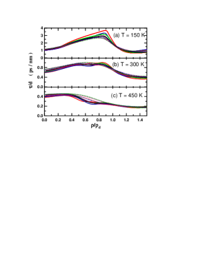
Carbon nanotube devices can be made with a range of nanotube diameters, offering different bandgaps. We find the scattering time to be approximately proportional to the diameter for all charge densities and temperatures. Indeed, the combination depends primarily on temperature and charge density and only weakly on diameter as shown in Fig. 2. (In the zero density limit, there is an additional simplification Perebeinos3 , .)
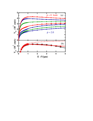
So far we have focused on the transport properties at low fields. Transport at high fields is also important, and our results for the dependence of carrier velocity on electric field are summarized in Fig. 3. For low carrier density, the drift velocity has a maximum at a field of 0.5-1.0 (V/m), which is within the range of fields used in normal device operation, and a negative differential mobility (NDM) at higher fields. The NDM becomes weaker with increasing density, and disappears entirely at a critical density . We find that is not a strong function of tube diameter ; for the range of considered here, 0.35-0.5 electrons/nm at room temperature. Above , the drift velocity is a monotonic function of electric field, with no saturation behavior up to the fields studied here disclaimer2 .
We can fit all the results in Fig. 3a using the following phenomenological formula:
| (6) |
where is the low-field mobility (from Fig. 1), and is the saturation velocity at . The value of (cm/s) is about of the Fermi velocity for graphene and it is roughly independent of tube diameter. The other two parameters, and , are fitted separately for each density.
A recent experiment ChenF at high drain voltage in CN-FETs (with 2.0-2.4 nm) gave a saturation velocity of cm/s. This is a factor of 2.5 smaller than the maximum velocity predicted in the zero density limit Perebeinos2 ; Pennington . The electrostatic gate capacitance per unit length was estimated to be F/m. This gives a charge density electrons/nm for the gate voltage of 9 V ChenF . This implies that the experimental device was in the regime, where the carrier density was well above critical density . Therefore, the zero density limit is not applicable, and the finite density result obtained from Fig. 3 agrees much better with the experiment.
Negative differential mobility has been predicted theoretically Pennington ; Perebeinos3 ; Verma and negative differential conductance has been observed experimentally Dai . One possible interpretation of this behavior Pennington ; Verma is that the occupation of the second band (which has higher effective mass) is responsible for the NDM. In agreement with previous studies Pennington ; Verma , we find that at high field a significant fraction of charge carriers occupy the second band. However, we find that this alone does not explain the NDM. In fact, if we artificially restrict the electrons to the first band, the NDM becomes stronger rather than weaker (Fig. 3b).
To understand the origin of the NDM, we examine the effect of changes in bandstructure. The tight-binding bandstructure is well described by a hyperbolic dispersion [Eq. (4)]; and Fig. 3b shows that the hyperbolic bandstructure gives results essentially identical to the real bandstructure (when only the first band is included). However, when we replace the realistic hyperbolic bandstructure with a parabolic band in Fig. 3b, the NDM disappears entirely. Therefore, we conclude that the non-parabolicity of the first band is responsible for the NDM in semiconducting carbon nanotubes.
In the NDM regime, the mobility is approximately constant over a wide range of electric field, and equal to the most negative value, i.e. the maximum NDM. Therefore, we can characterize the NDM of a given tube by two parameters: the most-negative value ; and the field at which the velocity reaches a maximum.
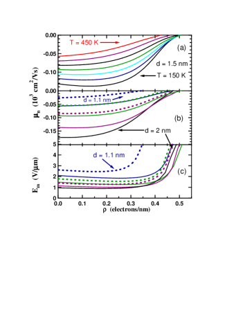
With these parameters, we can summarize the behavior over a range of density, different temperatures and tube diameters as shown in Fig. 4. As the temperature is increased, the maximum NDM decreases approximately linearly with temperature.
The maximum NDM, shown in Fig. 4b, increases with tube diameter and has a clear family effect. The family of tubes with mod have higher NDM than family of tubes with mod. This can be understood by the fact that the ratio measures the non-parabolicity of the band, which depends on the tube family. In the calculations for a single hyperbolic band Eq. (4), we find that the NDM is a linear function of , even though and are independent variables. If and coincide with the tight-binding values, the drift velocity is virtually the same as in the tight-binding band calculations restricted to a single band (as show in Fig. 3b).
Finally, the velocity reaches a maximum at a field shown in Fig. 4c, which decreases with the tube diameter. This suggests that conditions for the NDM are easier to achieve in larger diameter tubes. At the critical density , the field grows to infinity and NDM disappears.
In conclusion, we calculated the transport properties of CN-FETs as a function of change density as controlled by the gate potential. The low-field mobility dependence on the charge density is mainly determined by the scattering at low temperatures, and by both scattering and non-parabolicity of the first conduction band at high temperatures. At high fields, the drift velocity shows a negative differential mobility behavior which is large in large diameter tubes and low temperatures. We showed that the non-parabolicity of the first conduction band is responsible for the NDM behavior.
References
- (1) Electronic address: vperebe@us.ibm.com
- (2) Avouris, Ph. MRS Bulletin 2004, 29, 403; McEuen, P. L.; Fuhrer, M. S.; Park, H. IEEE Trans. Nanotech. 2002, 1, 78; Dai, H. J. Surface Science 2002, 500, 218.
- (3) Misewich, J. A.; Martel, R.; Avouris, Ph.; Tsang, J. C.; Heinze, S.; Tersoff, J. Science 2003, 300, 783.
- (4) Freitag, M.; Chen, J.; Tersoff, J.; Tsang, J. C.; Fu, Q.; Liu, J.; Avouris, Ph. Phys. Rev. Lett. 2004, 93, 076803.
- (5) Javey, A.; Guo, J.; Wang, Q.; Lundstrom, M.; Dai, J. Nature 2003, 424, 654.
- (6) Snow, E. S.; Novak, J. P.; Campbell, P. M.; Park, D. Appl. Phys. Lett. 2003, 82, 2145; Snow, E. S.; Campbell, P. M.; Ancona, M. G.; Novak, J. P. Appl. Phys. Lett. 2005, 86, 033105.
- (7) Bradley, K.; Davis, A.; Gabriel, J.-C. P.; Grüner, G. Nano Lett. 2005, 5, 845.
- (8) Dürkop, T.; Getty, S. A.; Cobas, E.; Fuhrer, M. S. Nano Lett. 2004, 4, 35.
- (9) Yao, Z.; Kane, C. L.; Dekker, C. Phys. Rev. Lett. 2000, 84, 2941.
- (10) Javey, A.; Guo, J.; Paulsson, M.; Wang, Q.; Mann, D.; Lundstrom, M.; Dai, H. Phys. Rev. Lett. 2004, 92, 106804.
- (11) Park, J. Y.; Rosenblatt, S.; Yaish, Y.; Sazonova, V.; Ustunel, H.; Braig, S.; Arias, T. A.; Brouwer P.; McEuen, P. L. Nano Letters 2004, 4, 517.
- (12) Zhou, X.; Park, J. Y.; Huang, S.; Liu, J.; McEuen, P. L. Phys. Rev. Lett. 2005, 95, 146805.
- (13) Chen, Y. F; Fuhrer, M. S. Phys. Rev. Lett. (to be published).
- (14) Perebeinos, V.; Tersoff, J.; Avouris, Ph. Phys. Rev. Lett. 2005, 94, 086802.
- (15) Pennington, G.; Goldsman, N. Phys. Rev. B 2003, 68, 045426.
- (16) Verma, A.; Kausera, M. Z.; Ruden, P. P. J. Appl. Phys. 2005, 97, 114319.
- (17) Guo, J.; Lundstrom, M. Appl. Phys. Lett. 2005, 86, 193103.
- (18) Electron-electron scattering is neglected here, since it does not change the net momentum of the interacting charge carriers.
- (19) Saito, R.; Kataura, H. in Carbon Nanotubes: Synthesis, Structure, Properties and Application, edited by Dresselhaus, M. S.; Dresselhaus, G.; Avouris, Ph. (Springer-Verlag, Heidelberg 2001), Vol. 80.
- (20) Aizawa, T.; Souda, R.; Otani, S.; Ishizawa, Y.; Oshima, C. Phys. Rev. B 1990, 42, 11469; ibid. 1991, 43, 12060.
- (21) Su, W. P.; Schrieffer, J. R.; Heeger, A. J. Phys. Rev. Lett. 1979, 42, 1698; Phys. Rev. B. 1980, 22, 2099.
- (22) Perebeinos, V.; Allen, P. B.; Pederson, M. Phys. Rev. A. 2005, 72, 012501.
- (23) Alternatively, the natural definition of and resulting definition of give almost identical result at low field.
- (24) At electric fields above a few V/m, the charge carrier can be accelerated to energies above the bandgap. This leads to impact excitation (as evidenced by an increase in electroluminiecence Jia ). This additional decay channel is not included in our description, and, therefore, we report the calculations for the fields up to (V/m) only.
- (25) Chen, J.; Perebeinos, V.; Freitag, M.; Tsang, J.; Fu, Q.; Liu, J.; Avouris, Ph. (unpublished).
- (26) Cao, J.; Wang, Q.; Wang, D.; Dai, H. Small 2005, 1, 138; Pop, E.; Mann, D.; Cao, J.; Wang, Q.; Goodson, K.; Dai, H. Phys. Rev. Lett. 2005, 95, 155505.