Charge sensing in carbon nanotube quantum dots on microsecond timescales
Abstract
We report fast, simultaneous charge sensing and transport measurements of gate-defined carbon nanotube quantum dots. Aluminum radio frequency single electron transistors (rf-SETs) capacitively coupled to the nanotube dot provide single-electron charge sensing on microsecond timescales. Simultaneously, rf reflectometry allows fast measurement of transport through the nanotube dot. Charge stability diagrams for the nanotube dot in the Coulomb blockade regime show extended Coulomb diamonds into the high-bias regime, as well as even-odd filling effects, revealed in charge sensing data.
Carbon nanotubes are promising systems on which to base coherent electronic devices McEuen et al. (1999); Liang et al. (2001); Biercuk et al. (2005a). Due to a combination of strong confinement, quantized phonon spectrum Hone et al. (2000), and zero nuclear spin, carbon nanotubes are likely to exhibit long-lived coherent states. Key to the success of this technology is the ability to manipulate electron states within a nanotube and perform fast, efficient readout. Recent advances in device fabrication Biercuk et al. (2005a); Javey et al. (2002, 2003); Biercuk et al. (2004, 2005) allow the creation of multiple quantum dots along the length of a tube with controllable coupling by applying voltage biases to electrostatic top-gates. However, readout of these structures has been limited to dc transport, which is invasive and slow compared to relevant coherence times Forro et al. (2000).
In this Letter, we describe the integration of superconducting aluminum radio frequency single electron transistors (rf-SETs) Schoelkopf et al. (1998) with carbon nanotube quantum dot devices defined by electrostatic gates Biercuk et al. (2005). The rf-SET serves as a sensitive electrometer Devoret and Schoelkopf (2000) and, when capacitively coupled to the nanotube dot, provides a means of non-invasively detecting its charge state on short timescales and in regimes not accessible with transport measurements DiCarlo et al. (2004); Lu et al. (2003); Buehler et al. (2005); Vandersypen et al. (2004); Elzerman et al. (2004). These represent the first charge sensing experiments with nanotube quantum dots using integrated charge detection. In addition, we make use of radio-frequency (rf) reflectometry that enables fast transport measurements of the nanotube correlated with fast charge sensing by the capacitively coupled rf-SET. Previous work Li et al. (2004) has used reflectometry to investigate the microwave impedance of nanotubes and transistor action at low (Hz) frequencies. The present study advances previous work by simultaneously carrying out charge sensing together with rf transport as well as by gaining five orders of magnitude in time resolution.
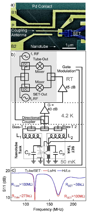
Carbon nanotubes were grown from patterned Fe catalyst islands on a Si/SiO2 wafer via chemical vapor deposition. Single-walled tubes with diameters less than nm were identified using atomic force microscopy and selectively contacted via electron beam lithography Biercuk et al. (2005a). Contacts made from nm of Pd Javey et al. (2003) were connected to larger metallic pads defined by optical lithography. The entire device was then coated with 35nm Al2O3 using low-temperature atomic layer deposition (ALD). Three top-gates were then aligned to each nanotube: two “barrier gates” (B1, B2) to deplete the underlying nanotube, defining a quantum dot, with a third “plunger gate” (P) between them to tune the energy of the dot (Fig. 1a) Biercuk et al. (2005). The doped Si wafer also serves as a global back-gate. Nanotubes that showed little gate response (presumably metallic) were not studied further. The SET island and the nanotube dot were capacitively coupled by a 50nm Ti/AuPd (20Å/30Å) antenna which crosses the tube and sits under the SET island. The aluminum SET was fabricated using double-angle evaporation on top of the coupling antenna (Fig 1a). Devices were mounted on a circuit board with rf coplanar waveguides and cooled in a dilution refrigerator with a base temperature of 30-50 mK. Electron temperature measured in a similar configuration was in the range 100-200 mK. Data from two integrated rf-SET/nanotube devices showing similar behavior are reported.
Charge sensing is performed by monitoring the resistance of the SET using rf-reflectometry. In the same way, direct transport measurements of the nanotube are made using a small () ac signal at rf frequencies (above 100MHz). A schematic of the setup, showing the generation of the reflectometry ‘carrier’ signals at frequencies and , is shown in Fig. 1b. The two carrier signals are combined onto a single transmission line and fed to a directional coupler at the 1K state of the dilution refrigerator. Two tank circuits transform the high resistance of the SET ( 50k) or nanotube ( 200k) towards , at the resonance frequencies set by the parasitic capacitance and series chip-inductor (nH for the nanotube and nH for the SET). At resonance, changes in resistance of either the nanotube or SET modify the -factor of the respective tank circuit and the amount of reflected rf-power. After amplification at 4K (40dB) and room temperature (45dB) the signals are homodyne detected using two mixers and two local oscillators. Low-pass filtered output voltages from each mixer are proportional to the change in respective device resistance. The use of frequency-domain multiplexing allows both the SET and nanotube to be monitored using a common transmission line and cryogenic amplifier Stevenson et al. (2002); Buehler et al. (2004). Bias-tees on the circuit board enable standard dc transport measurements of both devices.
Figure 1c shows reflected power from the tank circuits as a function of frequency measured with a network analyzer after amplification. The two resonances are identified at 120MHz for the nanotube and 165MHz for the SET. Bandwidths are MHz for the nanotube and MHz for the SET.
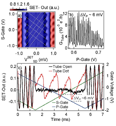
Figure 2a shows a charge stability plot for the SET used for all measurements in Figs. 2 and 3. Plotted is the demodulated voltage as a function of both the dc source-drain bias across the SET and the voltage applied to a nearby gate. The SET is typically operated at the threshold for quasi-particle transport, ( is the superconducting gap), where the rf-SET sensitivity is maximized. Similar rf-SET devices measured in this setup exhibited charge sensitivities better than Buehler et al. (2004).
We form a quantum dot in the carbon nanotube by applying appropriate voltages to gates B1 and B2 (Fig. 1a) with the back-gate set such that the nanotube is n-type. The section of the nanotube between depletion regions formed by gates B1 and B2 serves as the quantum dot. In this configuration, Coulomb blockade (CB) is observed using standard low frequency lock-in measurements, as a series of conductance peaks as a function of P-gate voltage Biercuk et al. (2005) (Fig. 2b).
The energy of the dot is changed on fast timescales by applying a triangle-wave voltage ramp to the P-gate. A compensating gate ramp is applied to the S-gate to maintain the SET at a fixed conductance value. When the P- and S-gates sweep together in the same direction, the SET is uncompensated and exhibits Coulomb blockade. In the region where the P- and S-gates sweep in opposite directions the SET is compensated and may be held at a position of maximum transconductance.
In the compensated configuration, the SET senses a characteristic sawtooth charging pattern associated with P-gate induced tunneling of electrons onto the dot. The period of the sawtooth in P-gate voltage is consistent with that measured directly from low frequency lock-in measurements of CB in the nanotube. By contrast, if the barrier gate voltages are set such that there is no dot formed in the tube, we observe a smooth line in the SET response (black trace, Fig. 2c). This indicates that the observed sawtooth response corresponds to charging of the gate-defined nanotube quantum dot. The magnitude of the charge signal induced on the SET with the addition of a single electron to the nanotube dot is , indicating strong coupling between the nanotube and the SET electrometer.
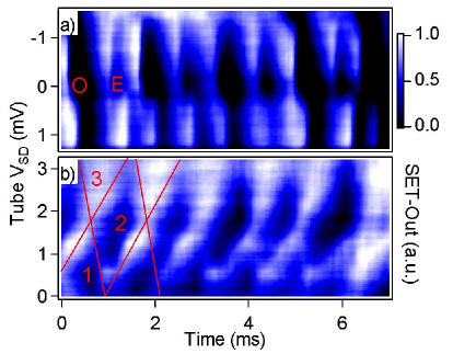
Plotting the (compensated) SET-Out signal as a function of time (as the P-gate voltage is ramped) and source-drain voltage across the tube reveals the familiar diamond pattern associated with Coulomb blockade (Fig. 3a). Here the applied voltage across the nanotube also couples capacitively to the SET itself. This effect is nulled by adding a compensating dc offset to the gate ramp. The nanotube dot charge configuration is fixed in the diamond regions (and current blocked), while the blockade is lifted and current flow allowed at sufficiently high values of . In appropriate biasing configurations of gates B1 and B2, we observe even-odd filling in the nanotube quantum dot Cobden et al. (1998), indicated by an alternating pattern of large and small diamonds. This is consistent with a shell-filling model in which a single electron can enter a discrete energy level in the dot with charging energy and quantum level spacing ( is the total dot capacitance). A second electron, with opposite spin to the first can enter the same orbital state requiring only . Estimating for a dot of the size used in this experiment to be using , where is the dot length, is consistent with experimental measurements. We have also observed four-fold shell filling Liang et al. (2002); Sapmaz et al. (2005) in these gated nanotube devices.
In addition to the low-bias diamonds commonly visible in transport, charge sensing enables detection of the Coulomb staircase in when one of the tunnel barriers is made much larger than the other. In this configuration consecutive Coulomb levels are populated from the source with increasing before tunneling to the drain can occur. Detection is possible because the SET senses the charge state of the nanotube dot and not the current that flows from source to drain, which can be immeasurably small when the resistance of one of the barriers is made large enough to observe the Coulomb staircase. In the SET sensing signal we observe diamonds centered at , the bias corresponding to the apex of the first order charging diamonds. First, second, and the beginning of third order diamonds are visible in Fig. 3b, each offset by from the center of the diamonds of the next lower or higher order foo .
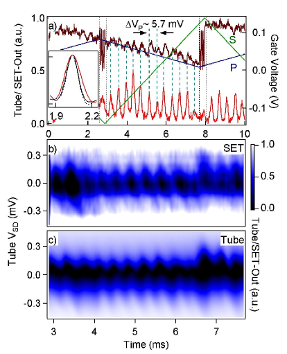
By monitoring the demodulated signals from the tube and SET simultaneously, we can correlate rf-transport and charge sensing. Figure 4a shows both the demodulated signal from the nanotube together with SET-Out for S- and P-gate ramps with the nanotube in the CB regime (different device from Figs. 2 and 3). CB peaks are evident in the signal from the tube, and a sawtooth pattern is visible in SET-Out, with sequential charge addition occurring on time scales of (we have performed similar measurements with charge addition periods , but systematic noise increased with gate speed). The two signals are correlated as expected, with the apex of each CB peak falling roughly in the middle of the charging sawtooth. Further, the width of the sharp transition region for each sawtooth is roughly equivalent in time to the width of the CB peak.
We have also studied how the biasing point of the SET influences the Coulomb blockade in the nanotube quantum dot. Consistent with measurements made on Al single-electron boxes Turek et al. (2005), we observe asymmetries and changes in the width of the CB peaks with varying across the SET (Inset Fig. 4a). This behavior is likely due to a combination of heating Kruprnin et al. (1999) and the backaction connected with charge fluctuations of the SET island as current flows from source to drain. We see a very slight narrowing of the Coulomb blockade peaks in the nanotube dot when the rf-SET is biased near the double Josephson quasi-particle peak (DJQP) Clerk et al. (2002), relative to the CB peak-width when the SET is biased into the superconducting gap. Separating back-action and heating effects will requires further study.
Charge stability plots for the nanotube quantum dot, constructed from both SET-Out (Fig. 4b) and Tube-Out (Fig. 4c) as a function of across the nanotube, show the nanotube (peaks) and SET (sawtooth) signals to be correlated. The rf-SET, however, is sensitive to charge fluctuations in regions of and P-gate voltage where direct transport measurements on the tube do not yield measurable currents, and where resistance changes in the nanotube mapped through reflected-rf are immeasurable.
The authors wish to thank D. Barber, R. Starrett and N. Court for technical assistance. This work was supported by ARO/ARDA (DAAD19-02-1-0039 and -0191 and DAAD19-01-1-0653), NSF-NIRT (EIA-0210736), and Harvard Center for Nanoscale Systems. M.J.B. acknowledges support from an NSF graduate research fellowship and an ARO-QCGR fellowship. D.J.R. acknowledges a Hewlett-Packard postdoctoral fellowship.
References
- McEuen et al. (1999) P. L. McEuen et al., Phys. Rev. Lett. 83, 5098 (1999).
- Liang et al. (2001) W. Liang et al., Nature (London) 411, 665 (2001).
- Biercuk et al. (2005a) M. J. Biercuk et al., Phys. Rev. Lett. 94, 026801 (2005).
- Hone et al. (2000) J. Hone et al., Science 289, 1730 (2000).
- Javey et al. (2002) A. Javey et al., Nature Mat. (London) 1, 241 (2002).
- Javey et al. (2003) A. Javey et al., Nature (London) 424, 654 (2003).
- Biercuk et al. (2004) M. J. Biercuk, N. Mason, and C. M. Marcus, Nano Lett. 4, 2499 (2004).
- Biercuk et al. (2005) M. J. Biercuk et al., Nano Lett. 5, 1267 (2005).
- Forro et al. (2000) L. Forro et al., Science and Application of Nanotubes. Kluwer Academic/Plenum Publishers, New York p. 297 (2000).
- Schoelkopf et al. (1998) R. J. Schoelkopf et al., Science 280, 1238 (1998).
- Devoret and Schoelkopf (2000) M. H. Devoret and R. J. Schoelkopf, Nature (London) 406, 1039 (2000).
- DiCarlo et al. (2004) L. DiCarlo et al., Phys. Rev. Lett. 92, 226801 (2004).
- Lu et al. (2003) W. Lu et al., Nature 423, 422 (2003).
- Buehler et al. (2005) T. M. Buehler et al., Appl. Phys. Lett. 86, 143117 (2005).
- Vandersypen et al. (2004) L. M. K. Vandersypen et al., Phys. Rev. Lett. 85, 4394 (2004).
- Elzerman et al. (2004) J. M. Elzerman et al., Nature (London) 430, 431 (2004).
- Li et al. (2004) S. Li, Z. Yu, and S.-F. Yen, Nano Lett. 4, 753 (2004).
- Stevenson et al. (2002) T. R. Stevenson et al., App. Phys. Lett. 80, 3012 (2002).
- Buehler et al. (2004) T. M. Buehler et al., J. Appl. Phys. 96, 4508 (2004).
- Cobden et al. (1998) D. H. Cobden et al., Phys. Rev. Lett. 81, 681 (1998).
- Liang et al. (2002) W. Liang, M. Bockrath, and H. Park, Phys. Rev. Lett. 88, 126801 (2002).
- Sapmaz et al. (2005) S. Sapmaz et al., Phys. Rev. B. 71, 153402 (2005).
- (23) We also observe higher order diamonds without compensating for the direct effect of on the SET, but over a smaller range of gate bias.
- Turek et al. (2005) B. A. Turek et al., arXiv:cond-mat/0501504 (2005).
- Kruprnin et al. (1999) V. A. Kruprnin et al., Phys. Rev. B 59, 10778 (1999).
- Clerk et al. (2002) A. A. Clerk et al., Phys. Rev. Lett. 89, 176804 (2002).