Current address: ]U.S. Army Research Laboratory, Aberdeen Proving Ground, Maryland 21005-5066.
Ab initio study of semiconducting carbon nanotubes adsorbed on the Si(100) surface: diameter- and registration-dependent atomic configurations and electronic properties
Abstract
We present the first ab initio study of semiconducting carbon nanotubes adsorbed on the unpassivated Si(100) surface. Despite the usual gap underestimation in density functional theory, a dramatic reduction of the semiconducting gap for these hybrid systems as compared with the electronic gaps of both their isolated constitutive components has been found. This is caused by the changes in the electronic structure as the surface reconstructs due to the tube’s proximity, the concomitant electronic charge transfer from the nanotubes, and the band hybridization with silicon and carbon states resulting in the appearance of states within the energy gap of the formerly isolated nanotube. Furthermore, it is determined that semiconducting nanotubes exhibit weaker adsorption energies and remain at a greater distance from the Si(100) surface as compared to metallic nanotubes of similar diameter. This effect may be useful for the solid-state separation of metallic and semiconducting nanotubes.
pacs:
68.35.-p,68.43.-h,68.43.Bc,73.22.-fI INTRODUCTION
First-principles studies illustrating the effect of technologically relevant semiconductor surfaces such as InAs,Kim et al. (2004a) GaAsKim et al. (2004b) and Si(100) on the electronic properties of single-wall carbon nanotubes (SWNTs) have been published recently. In the case of Si(100), the study was focused on determining the lowest-energy structural configuration and modifications to the electronic structure of a metallic (6,6) SWNT as a result of its interaction with this surface. This calculation was performed for a nanotube in the proximity to an either cleanOrellana et al. (2003, 2004) or selectively hydrogen-passivatedMiwa et al. (2005) Si(100) surface where the nanotube axis was parallel to the trench between adjacent Si dimer rows. Remarkably, there have been no studies of this system for semiconducting tubes, in different geometrical configurations, nor on the dependence of the properties of the hybrid system against nanotube diameter. These are relevant issues to be addressed, as experimental techniques permitting the ultra-clean deposition of SWNTs onto doped Si(100) and other semiconductor surfaces in ultra-high vacuum (UHV) at room temperature have been reported.Albrecht and Lyding (2003, 2004); Ruppalt et al. (2004) As contaminant-free atomistic manipulation becomes more feasible, the promise of molecular systems with tunable electronic and mechanical properties becomes a reality.
It is clear that near-term applications for carbon nanotubes in electronic and opto-electronic devices would benefit from their integration with conventional semiconductor platforms such as Si or GaAs. In this direction, rectifying carbon nanotube-silicon heterojunction arrays have been demonstrated,Tzolov et al. (2004) and semiconductor heterostructures of GaAs/AlAs and GaAs/MnAs have been used as electrical contacts to individual SWNTs.Jensen et al. (2004) Recent experimentsSu et al. (2000) showing the existence of two preferential directions for the growth of SWNTs on silicon surfaces indicate that there is a non-negligible interaction between the SWNT and its substrate. One relevant issue which remains to be addressed is the nature of the mechanical and electronic properties of the semiconductor-nanotube interfaces.
The subject of this work is the interaction between the unpassivated Si(100) surface and semiconducting carbon nanotubes using density functional theory (DFT).Hohenberg and Kohn (1964) Those studies are complemented with additional calculations on metallic nanotubes of comparable diameter. We study nanotubes that are in parallel or perpendicular orientations relative to the Si dimer row direction. We have found a striking and somewhat counter-intuitive reduction of the semiconducting gaps for these hybrid systems which are composed of two semiconductors. The nanotubes presented in this study have diameters between 5 and 12 Å. This work was comprehensive in order to find robust properties on these hybrid systems; in particular those independent of diameter and chirality as experiments do not have fine control of these variables yet.
Section II discusses the theoretical approximations employed and the structural configurations considered in this study. In Section III we show the resulting atomic configurations of the combined Si(100)-SWNT system, which have marked trends depending on the original electronic character of the SWNTs involved (metallic or semiconducting). Results from Voronoi and Hirshfield population analysisFonseca-Guerra et al. (2003) are also provided and show electronic charge being transferred from the nanotubes to the silicon slab. The resulting band structures at equilibrium, as well as the projected density of states (PDOS) over the atomic species involved are reported also. The PDOS indicates a clear hybridization of the bands between surface and nanotube states. This hybridization is further confirmed by depicting wavefunctions near the electronic gaps. Finally, we present the change in energy prior to the force minimization procedure, as the nanotubes are rotated about their axes in close proximity to the Si(100) surface. Conclusions are presented in Section IV.
II methods
Our calculations in the local density approximationKohn and Sham (1965) (LDA) were performed with the SIESTA code.Soler et al. (2002) The exchange-correlation potential employed is the one parameterized by Perdew-Zunger,Perdew and Zunger (1981) based on the Ceperley-Alder data.Ceperley and Alder (1981) Core electrons are replaced by norm-conserving Troullier-Martins pseudopotentials.Troullier and Martins (1991) For greater variational freedom, a double- basis set for and orbitals, and a single- basis set for orbitals was constructed using the prescription of Junquera et al.Junquera et al. (2001) To ensure the flexibility in our basis sets, their parameters were optimized by means of the simplex algorithm Press et al. (1992) on graphite and diamond for the carbon basis, while the silicon basis was optimized only in the diamond structure. As the hydrogen atoms only served to passivate dangling bonds, the hydrogen basis was not optimized. As shown in Table 1, the lattice constants obtained from the optimized bases compare well with previous theoretical estimates.
We use the p(22) reconstruction of the Si(100) surface for calculations involving semiconducting SWNTs. The gap obtained is of 0.235 eV. In all cases a slab with six silicon monolayers with a height of 7.81 Å was employed. The bottommost layer is hydrogen(H)-passivated forming a dihydride arrangement. The SWNTs will be placed in proximity of the uppermost unpassivated layer. The area of the unit cell is with Å. The vacuum region in the vertical direction is fixed in order to provide at least Å separation between periodic images when the SWNTs are in place.
Since we are interested in trends that could complement both experimental work in this area and published theoretical results on metallic SWNTs on this surface the SWNTs chosen satisfy the following criteria:
-
1.
They are semiconducting.
-
2.
Their diameter is of the order of 10 Å.
-
3.
They are commensurate with the underlying surface.
While (,) (metallic) SWNTs happen to be commensurate to within 3% with the underlying Si(100) surface,Orellana et al. (2003) the shortest commensurate semiconducting SWNT, of indexes (3,) –and with integer– would be 15.391 Å long. The large unit cell sizes involved in calculations have deterred researchers from performing calculations in this system with semiconducting nanotubes. Table 2 lists the nanotubes studied, their diameters, lengths as well as their DFT gaps. Tubes with chiral indexes (2,) are 11.294 Å long, so a supercell constructed out of two nanotube unit cells is required in this case to meet the surface’s supercell length. Thus the slab supercells required for calculations involving both the surface and semiconducting nanotubes have surface areas equal to or , depending on the length of the SWNT, its diameter and the surface reconstruction employed. This choice leaves more than 10 Å between nanotube images.
| Nanotube | Diameter (Å) | Length (Å) | DFT Gap (eV) |
|---|---|---|---|
| (6,2) | 5.657 | 15.391 | 0.860 |
| (8,4) | 8.302 | 11.294 | 0.945 |
| (12,4) | 11.314 | 15.391 | 0.699 |
| (9,3) | 8.486 | 15.391 | 0.000 |
| (6,6) | 8.153 | 2.465 | 0.000 |
In order to test the accuracy of our calculations against published results,Orellana et al. (2003, 2004) benchmark calculations on a chiral metallic SWNT interacting with c(4x2) reconstructed Si(100) surface were performed. The surface gap in this case is equal to 0.223 eV. The c(42) reconstruction minimizes the total energy the most and therefore is the best candidate for the surface reconstruction.Healy et al. (2001) The metallic (9,3) SWNT is comparable in diameter to the (6,6) SWNT studied extensively by Orellana et al.Orellana et al. (2003, 2004); Miwa et al. (2005) Due to the surface reconstruction used and the requirement for the nanotube images to be separated by at least 10 Å this required an even larger, area for the underlying surface. This benchmark calculation is also used to assess the effect of chirality and the exchange-correlation approximation; LDA in this work and GGA in Refs. Orellana et al., 2003, 2004; Miwa et al., 2005.
III Results
| Nanotube: | (6,2) | (8,4) | (12,4) | (9,3) |
|---|---|---|---|---|
| h | 0.15 | 0.11 | 0.03 | 0.14 |
| h | 0.18 | 0.29 | 0.41 | 0.44 |
| h | 0.20 | 0.15 | 0.09 | 0.43 |
| h | 0.05 | 0.06 | 0.04 | 0.00 |
| h | 0.13 | 0.26 | 0.16 | 0.36 |
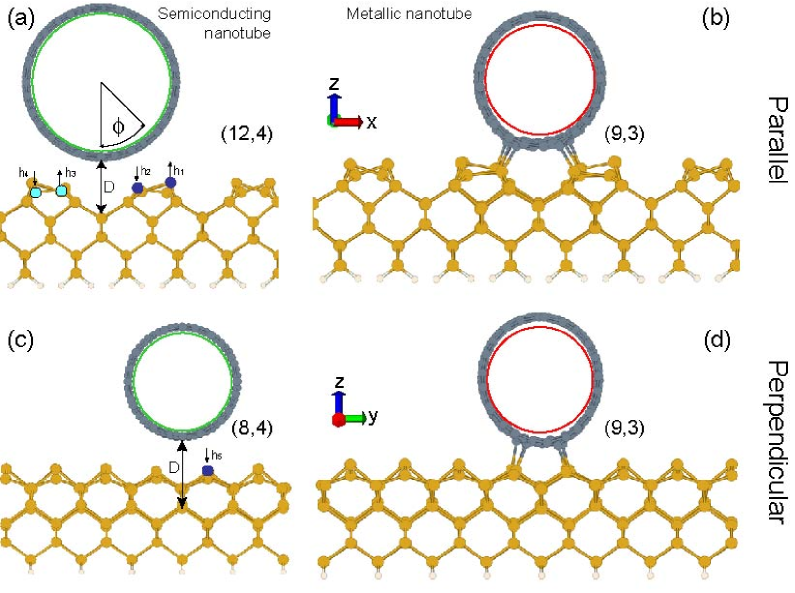
Figure 1 shows hybrid structures with maximum residual forces less than 0.02 eV/Å. The relevant geometric parameters are the minimum distance between the SWNT and the dimer trench, the vertical atomic displacements resulting from the reconfiguration of the silicon atoms closest to the SWNT, and the azimuthal rotation angle . We want to emphasize the shorter bond lengths between the carbon and silicon atoms when the metallic tubes are involved, as well as a marked distortion of the nanotube, emphasized by the inner (red) circle. In comparison, semiconducting tubes are in equilibrium farther away from the surface and do not change their circular profile, as evidenced by the (green) inner circle perfectly matching the nanotubes’ perimeters. To contrast with published work,Orellana et al. (2003, 2004) due to chirality the metallic nanotube in either configuration studied showed only seven bonds of varying lengths (2.03–2.27 Å in the parallel configuration and 2.02–2.15 Å in the perpendicular configuration). For the semiconducting nanotubes, the shortest distance between carbon and silicon atoms turned out to be 2.62 Å and 2.87 Å for the (6,2) tube in the parallel and perpendicular configuration, respectively. All the semiconducting tubes with larger diameters had their carbon atoms more than 2.84 Å away from the closest surface silicon atom and in most cases more than 1 Å above the distance in the C–Si bond of silicon carbide. This is indicative of a weaker bonding for semiconducting nanotubes adsorbed on the Si(100) surface. For chiral nanotubes, the optimal geometrical configuration can not be known a priori, but it has to come out after a sweeping through all angles ; this angular dependence is not as pronounced for semiconducting SWNTs. A detailed discussion follows.
III.1 Optimized atomic configurations
An equivalent plane-wave cutoff of 200 Ry was used to calculate the charge density on the real-space grid. To obtain the optimal configuration of these systems, we used a grid with a single -point (the –point), except for the (6,2) nanotube, where a 221 Monkhorst-PackMonkhorst and Pack (1976) (MP) grid was already employed for obtaining the relaxed structures. The adsorption energies were then calculated with a 221 MP grid.
III.1.1 Distance from the SWNTs to the silicon surface and surface reconfiguration
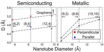
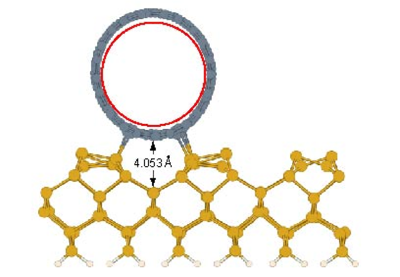
Total energies for the hybrid SWNT-Si(100) system with the SWNTs listed in Table 2 were calculated as a function of the distance from the nanotubes to the bottom of the the dimer trench. The optimal distance is reached when the total energy is at the global minimum. While holding the bottom hydrogen layer fixed, the hybrid structures were relaxed by a conjugate-gradient method to minimize the residual forces until they no longer exceeded 0.02 eV/Å. We also calculated the optimal distance for (8,8) and (10,10) SWNTs for a fixed angle in order to visualize and distinguish trends between semiconducting and metallic SWNTs. No relaxation procedure was performed on the latter tubes. Under relaxation those distances would decrease slightly, but the trend indicated here will stand. It should also be mentioned that the trend obtained in Fig. 2 for metallic tubes remained the same when the c(42) reconstructed surface was replaced by a p(22) reconstructed surface. This means that the distinct trends observed in Fig. 2 are due to the different electronic character of the nanotubes involved, and not to the surface reconstruction employed. This is stressed in Fig. 3, where the structural configuration of the (9,3) tube and the p(22) reconstructed surface with maximum residual forces down to 0.02 eV/Å, appears extremely similar to the one found for this nanotube on the c(42) reconstructed surface.
The diameter of the nanotube as well as its electronic character (metallic, semiconducting) are the determining factors on the relative distance between the nanotube and the surface. As the nanotube diameter increases, the distance from the SWNTs to the bottom of the dimer trench also increases asymptotically towards 5.52 Å, which is the limiting distance from the bottom of the Si dimer trench to a graphene plane (nanotube diameter ), indicated by the gray line in Fig. 2.111In order to obtain the separation between the surface and the graphene plane, we constructed silicon surface of area . A graphene surface can be placed on top in which the vector is perpendicular to the dimer trench, with a 3% elongation of the graphene plane in both perpendicular directions ( and are the graphene lattice vectors). We then found a minimal energy by varying the separation between the graphene plane and the relaxed surface. The results in Fig. 2 show that metallic nanotubes exhibit a stronger diameter dependence on their optimal distance to the surface’s slab.222This dependence of on the nanotube’s diameter is overlooked in Reference Orellana et al., 2003. In previous work, the same distance to the surface was used for the (6,6) SWNT and a tube of 100 Å in diameter, in an attempt to explain experimental results of multiwalled SWNTs on H-passivated surfaces.Hertel et al. (1998) We speculate that the adsorption energy of nanotubes on an H-passivated surface should be lower than the one corresponding to an unpassivated surface, because the dangling bonds of the silicon surface are hydrogen passivated. This effect is worthy of further investigation, but is not included in this present study. For the semiconducting nanotubes studied the diameter dependence is not as marked. Yet, Fig. 2 shows that a semiconducting SWNT in the perpendicular configuration will be about 0.5 Å farther away from the silicon surface in comparison with its equilibrium distance in the parallel configuration, in accordance with experimental observation.Albrecht and Lyding (2005)
The electronic properties of the Si(100) surface are closely related to its atomic configuration. Table 3 gives the average vertical displacements that the silicon atoms closer to the SWNT undergo due to the proximity of the SWNT. The Si(100) surface in the proximity of the SWNT is subject to a striking atomic reconfiguration. For a given SWNT the amount of surface reconfiguration is always greater in the parallel case. This is consistent with the fact that tubes in the parallel configuration stay closer to the surface (Fig. 2) and therefore interact more strongly than in the perpendicular case. We have to stress here that after atomic relaxation the semiconducting nanotubes undergo almost no structural change but remain very stiff. This is not the case for the metallic nanotube, as previously indicated.
III.1.2 Relative strength of the C-Si bonds
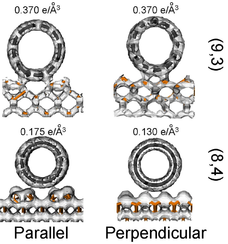
With the goal of visually expressing the varying strengths of bonds formed between carbon and silicon atoms for the metallic and semiconducting SWNTs, we show in Fig. 4 charge density isosurfaces for the (9,3) and (8,4) SWNTs. Results for the remaining nanotubes can be found in Table 4. Very dense bonds can be seen for the (9,3) SWNT in either configuration with the 0.37 /Å3 isosurface. The charge density isosurfaces show that the C–Si bonds are as strong as the Si–Si and C–C bonds in the surface and the nanotube, respectively, as can be inferred from the similar width.
| Nanotube: | (6,2) | (8,4) | (12,4) | (9,3) |
|---|---|---|---|---|
| Parallel | 0.235 | 0.175 | 0.120 | 0.370 |
| Perpendicular | 0.155 | 0.130 | 0.115 | 0.370 |
In order to understand the varying strengths of the bonds and the role of chirality on bond formation, refer to Fig. 1b, depicting the (9,3) SWNT in the parallel configuration. In this figure, surface dimers are located in the (,) plane. For the shortest bond (2.03 Å) the relative coordinates of the involved carbon and silicon atoms are (, , )=(1.00, 0.23, 1.75) Å. The second closest carbon atom to a surface silicon atom has relative coordinates equal to (0.99, 0.35, 1.76) Å, giving a bond length of 2.05 Å. Although the cartesian projections and are very similar in both cases, chirality breaks the mirror symmetry with respect to a plane formed by the SWNT axis and the bottom of the dimer trench once all bonds are considered (recall that only seven –instead of eight– bonds were formed), but it also shifts the carbon atoms by varying distances , according to their positions in the SWNT unit cell. Contrast this to the more symmetric configurations previously studied for the (6,6) SWNT in which pairs of bonding atoms have the same and a similar value for for all bonds due to mirror symmetry.
For the (8,4) SWNT we had to lower the density to 0.175 /Å3 to identify bond formation in the parallel configuration. Lower density through bonds will reflect the weaker adsorption energies found for semiconducting SWNTs. Notice that this isosurface does not form bonds in the perpendicular configuration. It is at the lower 0.130 /Å3 density when a single isosurface connecting the nanotube and slab can be seen. This is about a third of the density present in the strongest C–Si bond for the metallic SWNT. In conclusion, bond formation will be weaker for semiconducting SWNTs, and the weakest bond occurs for semiconducting SWNTs in the perpendicular configuration. These results are consistent with all findings of previous subsections.
III.1.3 Amount of charge transferred to the silicon slab
The results from Voronoi and Hirshfield deformation density charge analysisFonseca-Guerra et al. (2003) are summarized in Table 5. Because of the way they are defined, the results from those methods are independent of the numerical orbital basis, and they are also more meaningful physically: The Voronoi deformation density charge for a given atomic nucleus, for instance, is the absolute charge defined in the volume defined by all the points closer to that atomic nucleus than to any other nuclei. In all instances, the charge is transferred from the nanotube to the slab, and the magnitude of the charge transferred is larger when the tubes are parallel and on top of the dimer trench.
| Nanotube | Parallel | Perpendicular |
|---|---|---|
| (6,2) | +0.052 (+0.046) | +0.033 (+0.029) |
| (8,4) | +0.055 (+0.049) | +0.035 (+0.033) |
| (12,4) | +0.072 (+0.065) | +0.035 (+0.031) |
| (9,3) | +0.064 (+0.083) | +0.058 (+0.043) |
III.2 Ab initio electronic properties of the hybrid Si(100)-SWNT system
III.2.1 Band structures and densities of states
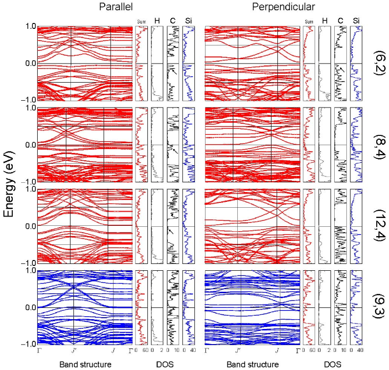
In order to have reliable band structures a stringent force relaxation was performed. As mentioned in Section III.1, the atomic positions were subject to a force minimization procedure with a single -point (the point), with the exception of the (6,2) SWNT, where a 221 MP grid was employed. The relaxed atomic positions from this calculation were then used in computing the band structures and PDOS. The band structures were obtained with a 441 MP grid, while the PDOS was computed from at least a 12121 MP -point grid (for example, the results for the (12,4) nanotube in the parallel configuration were obtained with a 24121 MP grid), using the converged self-consistent charge density obtained from the calculation with a 441 MP grid. The band structures and PDOS are depicted in Fig. 5. In all the plots shown in this figure the SWNT was placed parallel to the direction. For the PDOS a Gaussian smearing of 10 meV half-height width and 300 sampling points in the () eV energy interval were employed. The Gaussian smearing is in most cases smaller than the electronic gaps obtained from the band structures.333The choice of Gaussian smearing is consequent with the k-point sampling employed. In particular, a finer Gaussian smearing requires a concurrent finer mesh and it is beyond our computational capabilities. The PDOS is computed with a finer mesh, independently from the band structure calculation and indicates the contribution of each atomic species to the band structure.
| Nanotube: | (6,2) | (8,4) | (12,4) | (9,3) |
|---|---|---|---|---|
| Parallel | 0.099 | 0.008 | 0.033 | 0.000 |
| Perpendicular | 0.083 | 0.013 | 0.040 | 0.000 |
The two columns in Fig. 5 correspond to the relaxed hybrid system in either the parallel or perpendicular configurations. The most salient feature from Fig. 5, as the band structures indicate, is the dramatic reduction of the gap for the hybrid systems composed of semiconducting nanotubes (with gaps of at least 699 meV when isolated) and the Si(100) surface (with a gap bigger than 200 meV). The biggest gap found occurred for the system involving the (6,2) nanotube, and is equal to 83 meV. Refer to Table 6 for a comprehensive list of the electronic gaps. The projected densities of states in Fig. 5 indicate a contribution from the carbon orbitals to the band structure at energy values where the gap of isolated tubes is expected, highlighted by the arrows on the carbon PDOS (note the different scales for each species in the PDOS). We believe this reduction of the gap for the hybrid system with respect to the gaps of its constituent subsystems will occur even when more accurate quasiparticle (e.g. GW) calculations and experimental data are in place. Notice that, despite the strong structural modification observed for the metallic tube (Figs. 1b and 1d), this is insufficient in this case to open a gap in either configuration; refer particularly to Fig. 6 where we zoomed the band structure about the Fermi level in the parallel case, to better appreciate this fact.
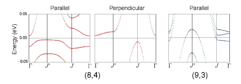
The reader might appreciate the existence of a single band above the Fermi energy for the system involving the (8,4) SWNT in the perpendicular configuration. The PDOS indicates a couple of dips and the density at those dips is not equal to zero. The discrepancy here only comes due to the insufficient number of -points employed. This system has the largest number of atoms, and we are certain a calculation with a finer mesh will result in a flatter PDOS in the region of interest, but we did not pursue further calculations due to their expensive nature. In the same note, the computational cost involved in computing a PDOS for the zoomed bands, which requires a finer smearing and a correspondingly increased number of -points, prevents us from performing such calculation. Nevertheless we are certain of the accuracy of the band structure, and therefore of the accuracy of the electronic gaps for the hybrid system with a (8,4) tube adsorbed. Experimentally, the gaps for the nanotubes could be obtained accurately on the inert H-passivated substrate, prior to hydrogen depassivation; the surface gap can be measured by a host of experimental techniques. The dramatic reduction of the gap in this hybrid system as well as the distinct structural trends for semiconducting and metallic nanotubes are the main findings of our investigations.
In Ref. Berber and Oshiyama, 2006 a gap opening for the small-diameter and achiral (5,5) nanotube was found in the perpendicular configuration. Due to a lesser symmetry in chiral tubes, which translates in longer bond lengths and a more complex atomic reconstruction and band hybridization, this effect is not seen in the (9,3) nanotube reported on this paper, and certainly more systematic studies would be required to address such a rather interesting effect; particularly with regards to knowing if it is robust enough to be observed in other nanotubes. Our work indicates that any semiconducting nanotube on this semiconductor surface results in a hybrid system with a gap smaller from that of the isolated constituent subsystems.
III.2.2 Highest occupied, and lowest unoccupied electronic states for the Si(100)-SWNT system
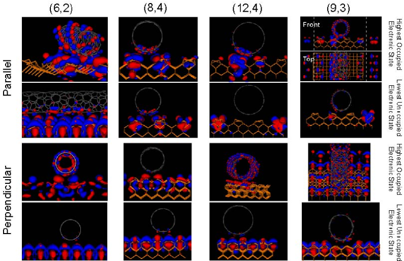
Wavefunctions for electronic states at the -point that are just below and above the Fermi energy –the (-point) Highest Occupied and Lowest Unoccupied Electronic States (HOES/LUES)– are depicted in Fig. 7. From those plots we observe that the electrons responsible for metallicity are either (a) extended over both the SWNT and the silicon slab; (b) predominantly over the silicon slab or (c) confined to the SWNT. We also found an instance –the (12,4) SWNT in the parallel configuration– in which the wavefunction is localized at the interface between the nanotube and the surface. In most cases involving the semiconducting nanotubes a more pronounced contribution from the nanotube to the HOES is seen in contrast with a more surface-like LUES. Those findings can be understood in terms of the relative contributions to the band structure from the carbon and silicon orbitals as seen from the PDOS in Fig. 5.
III.3 Adsorption energies
Adsorption energies on the Si(100) surface for the carbon nanotubes in this study are presented in Table 7. The adsorption energies are obtained as the difference between the total energies in the relaxed hybrid structures and those of the fully relaxed tubes and surface in the same supercell separated by 10 Å. Notice the constant adsorption energy for semiconducting nanotubes in the perpendicular configuration, and the decreasing adsorption energy with increasing diameter for semiconducting tubes in the parallel configuration. These two trends meet for a tube with diameter in between the (8,4) and (12,4) nanotubes, after which a semiconducting tube in the perpendicular configuration has a stronger adsorption energy. This is stressed by the bold font in Table 7.
| Nanotube: | (6,2) | (8,4) | (12,4) | (9,3) |
|---|---|---|---|---|
| Parallel | 0.20 | 0.18 | 0.11 | 0.63 |
| Perpendicular | 0.15 | 0.15 | 0.15 | 0.60 |
In order to determine the best angular ‘starting’ structure a chiral nanotube has to be rotated about its axis. Chirality precludes a highly symmetric configuration, potentially with the lowest energy, from being easily visualized. The energies as a function of with no atomic relaxation were obtained, and the difference of those energies with respect to the energy of a system where the tubes and surface are 10 Å apart are reported (this is called the energy gain and it is not an adsorption energy as the structures are not fully relaxed). The results are shown in Fig. 8, where the lower curves (red squares) refer to SWNTs in the perpendicular configuration. The upper curves (blue triangles) refer to the SWNTs in the parallel configuration. For our chiral tubes, the range of angles is given by , where GCD is the greatest common divisor of and . This range gives the maximum angular freedom that the nanotubes will have before the position of their carbon atoms becomes periodic. Notice the almost complete independence on for this energy for all semiconducting tubes, due to their weaker bonding as compared with metallic nanotubes. The (6,2) nanotube with the smallest studied diameter shows the most pronounced oscillations. This is due to its close proximity to the Si(100) surface that can greatly modify its energy as carbon and silicon atoms are brought closer to each other as a result of the tube’s rotation about its own axis. The distinctive trend for the metallic tube indicates an optimal configuration in which an extra bond (for a total of eight bonds) might form when full relaxation is performed. All the previous results shown in this paper were obtained at . Despite the fact that the metallic tube might not be in optimal angular configuration, our results are the first to date to show distinctively different trends for semiconducting and metallic nanotubes. In fact, once the metallic tube is in its optimal configuration, the trends provided here will only be accentuated.
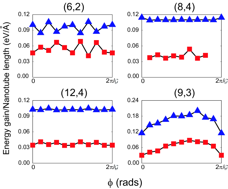
In the previously studied cases (Refs. Orellana et al., 2003, 2004; Miwa et al., 2005), the highly symmetric atomic arrangement of the achiral (6,6) SWNT with respect to the underlying surface silicon atoms results in optimal angular configurations in which is a function of . We consider that in a more general setting, chirality precludes such a highly symmetric configuration from occurring: the relative position of carbon atoms closest to the surface with respect to surface silicon atoms becomes a complicated function of the chiral angle. In Fig. 8 we observe a small energy dependence per unit length (of the order of 100 meV/Å) against the tube’s angle of rotation . This justifies the angular sweeping at fixed for our chiral SWNTs.
It is also apparent from Fig. 8 that the metallic nanotube displays an energy dependence on the angle of rotation twice as large as the semiconducting SWNTs. This is consistent with the fact that metallic tubes stay closer to the surface in comparison to semiconducting nanotubes of the same diameter. This could also be influenced by the different surface reconstruction we employed.
The prominent difference in the adsorption energies presented in Table 7 suggests a mechanism for the separation between semiconducting and metallic nanotubes in solid phase over this diameter range, provided they are always adsorbed in configurations with the greatest energy gain. Experimental techniques for nanotube separation to date rely on the chemistry and dipole moments of samples in solution.Krupke et al. (2003); Strano et al. (2003)
IV conclusions
We have studied semiconducting SWNTs adsorbed on the Si(100) surface. We used the results from the (9,3) SWNT, which compare well to previous published results for metallic SWNTsOrellana et al. (2003, 2004) as a test bed for our choice of exchange-correlation potential and surface reconstruction. Semiconducting SWNTs of the diameter range studied are placed at an almost constant distance to the surface. Those tubes are 0.5 Å closer to the surface when they are above and aligned with the trench between adjacent dimer rows, in comparison with any other configuration in which the trench and the tube axis do not align. We found a weak angular dependence on the adsorption energy of the system, and we believe this dependence will be further lowered as the length of the nanotube’s unit cell increases, due to the loss of symmetry in the relative positions of the carbon atoms in the SWNT closest to the Si(100) surface atoms. For the (9,3) SWNT, we found in agreement with Refs. Orellana et al., 2003, 2004 that it remains metallic in either configuration, but the weak angular dependence tells us it will remain at an almost fixed height , independent of its angular orientation. We also found a smaller adsorption energy for semiconducting SWNTs in comparison to metallic SWNTs of similar diameter, consistent with weaker bonding.
The electronic properties of these hybrid systems will vary in a qualitative way according to the relative orientation of the SWNT (parallel, perpendicular) with respect to the surface, but we find from our calculations that the system composed of semiconducting tubes on the semiconducting Si(100) surface displays dramatically smaller gaps in comparison with the isolated semiconducting systems that compose it, in both studied configurations. This reduction of the semiconducting gap can be ascribed to the modification of the band structure due to the surface reconfiguration, electronic charge transfer from the nanotubes and the resulting band hybridization from carbon states at energies where the gap appears for isolated tubes, as the PDOS indicates. The HOES for the hybrid systems can be extended, located predominately over either the silicon slab or the SWNT, or be localized at the interface between the SWNT and the Si(100) forming a one-dimensional conduction channel. In contrast, the LUES tend to be more localized towards the surface when semiconducting nanotubes are brought into proximity. Currently, experimental results on this system are starting to emerge.Albrecht and Lyding (2005) We hope that the results provided in this paper motivate further experimental work in the area, as the properties described in here might be useful for electronic as well as opto-electronic applications.
Systematic studies as the one presented here are truly necessary in order to assess robust properties of this hybrid system against properties that might appear for a given choice of chiral angles and geometrical configuration. In our case, the gap reduction appears for both configurations, and the bonding lengths are found to be consistently larger for semiconducting nanotubes in comparison with metallic ones. This implies a reduced absorption energy for semiconducting nanotubes on this surface. In turn, this might serve to mechanically attach metallic nanotubes and release semiconducting ones by suitable heating under dry conditions.Krupke et al. (2003); Strano et al. (2003)
ACKNOWLEDGMENTS
G. Bauer and G. Lopez-Walle assisted during the early stages of this project. We thank R. M. Martin, N. Tayebi, K. Ritter, H. Terrones and J. Junquera for useful discussions. M. Pruneda assisted us in performing the Voroni and Hirshfield charge analysis. These additional SIESTA routines were written by P. Ordejón. Calculations were performed on the CSE mac OS X Turing cluster, linux CEG cluster (U. Ravaioli, Z. Yang). This work was supported by National Computational Science Alliance under grant number DMR050032N (NCSA’s IBM pSeries 690 Copper cluster) and the Office of Naval Research, grant N00014-98-1-0604. S. B.-L. acknowledges partial funding from CONACyT (Mexico), P.M.A. a NDSEG graduate fellowship and N.A.R. grants from NSF (DMR-0325939) and DoE (DEFG02-91ER45439).
References
- Kim et al. (2004a) Y.-H. Kim, M. J. Leben, and S. B. Zhang, Phys. Rev. Lett. 92, 176102 (2004a).
- Kim et al. (2004b) Y.-H. Kim, M. J. Heben, and S. B. Zhang, AIP Conf. Proc. 772, 1031 (2004b).
- Orellana et al. (2003) W. Orellana, R. H. Miwa, and A. Fazzio, Phys. Rev. Lett. 91, 166802 (2003).
- Orellana et al. (2004) W. Orellana, R. H. Miwa, and A. Fazzio, Surf. Sci. 566-568, 728 (2004).
- Miwa et al. (2005) R. H. Miwa, W. Orellana, and A. Fazzio, Appl. Phys. Lett. 86, 213111 (2005).
- Albrecht and Lyding (2003) P. M. Albrecht and J. W. Lyding, Appl. Phys. Lett. 83, 5029 (2003).
- Albrecht and Lyding (2004) P. M. Albrecht and J. W. Lyding, AIP Conf. Proc. 723, 173 (2004).
- Ruppalt et al. (2004) L. B. Ruppalt, P. M. Albrecht, and J. W. Lyding, J. Vac. Sci. Technol. B 22, 1071 (2004).
- Tzolov et al. (2004) M. Tzolov, B. Chang, A. Yin, D. Straus, and J. M. Xu, Phys. Rev. Lett. 92, 075505 (2004).
- Jensen et al. (2004) A. Jensen, J. R. Hauptmann, J. Nygard, J. Sadowski, and P. E. Lindelof, Nano Lett. 4, 349 (2004).
- Su et al. (2000) M. Su, Y. Li, B. Maynor, A. Buldum, J. P. Lu, and J. Liu, J. Phys. Chem. B 104, 6505 (2000).
- Hohenberg and Kohn (1964) P. Hohenberg and W. Kohn, Phys. Rev. 136, B864 (1964).
- Fonseca-Guerra et al. (2003) C. Fonseca-Guerra, J.-W. Handgraaf, E. J. Baerends, and F. M. Bickelhaupt, J. Comput. Chem. 25, 189 (2003).
- Kohn and Sham (1965) W. Kohn and L. J. Sham, Phys. Rev. 140, A1133 (1965).
- Soler et al. (2002) J. M. Soler, E. Artacho, J. D. Gale, A. Garcia, J. Junquera, P. Ordejon, and D. Sanchez-Portal, J. Phys.: Condens. Matter 14, 2745 (2002).
- Perdew and Zunger (1981) J. P. Perdew and A. Zunger, Phys. Rev. B 23, 5048 (1981).
- Ceperley and Alder (1981) D. M. Ceperley and B. J. Alder, Phys. Rev. Lett. 45, 566 (1981).
- Troullier and Martins (1991) N. Troullier and J. L. Martins, Phys. Rev. B 43, 1993 (1991).
- Junquera et al. (2001) J. Junquera, O. Paz, D. Sanchez-Portal, and E. Artacho, Phys. Rev. B 64, 235111 (2001).
- Press et al. (1992) W. H. Press, S. A. Teukolsky, W. T. Vetterling, and B. P. Flannery, Numerical recipes in fortran 77, vol. 1 of Fortran Numerical Recipes (Cambridge U. Press, 1992), 2nd ed.
- Aschcroft and Mermin (1976) N. W. Aschcroft and N. D. Mermin, Solid State Physics (Harcourt College Publishing, Fort Worth, 1976), p. 76.
- Kganyago and Ngoepe (2003) K. R. Kganyago and P. E. Ngoepe, Phys. Rev. B 68, 205111 (2003).
- Healy et al. (2001) S. B. Healy, C. Filippi, P. Kratzer, E. Penev, and M. Scheffler, Phys. Rev. Lett. 87, 016105 (2001).
- Monkhorst and Pack (1976) H. J. Monkhorst and J. D. Pack, Phys. Rev. B 13, 5188 (1976).
- Hertel et al. (1998) T. Hertel, R. E. Walkup, and P. Avouris, Phys. Rev. B 58, 13870 (1998).
- Albrecht and Lyding (2005) P. M. Albrecht and J. W. Lyding, unpublished (2005).
- Berber and Oshiyama (2006) S. Berber and A. Oshiyama, Phys. Rev. Lett. 96, 105505 (2006).
- Krupke et al. (2003) R. Krupke, F. Hennrich, H. v. Lḧneysen, and M. M. Kappes, Science 301, 344 (2003).
- Strano et al. (2003) M. S. Strano, C. A. Dyke, M. L. Usrey, P. W. Barone, M. J. Allen, H. Shan, C. Kittrell, R. H. Hauge, J. M. Tour, and R. E. Smalley, Science 301, 1519 (2003).