Electron scattering in atomic force microscopy experiments.
Abstract
It has been shown that electron transitions, as measured in a scanning tunnelling microscope (STM), are related to chemical interactions in a tunnelling barrier. Here, we show that the shape and apparent height of subatomic features in an atomic force microscopy (AFM) experiment on Si(111) depend directly on the available electron states of the silicon surface and the silicon AFM tip. Simulations and experiments confirm that forces and currents show similar subatomic variations for tip-sample distances approaching the bulk bonding length.
pacs:
72.10.Bg,72.15.Eb,73.23.HkThe intense research into improving the local and energy resolution in scanning probe microscopes (SPM) over the last two decades have made the assignment of atomic features to the position of surface ions, at least in principle, a routine task. The very high resolution of individual features, today below the limit of one Ångstrom, makes it possible to carry out detailed studies of the electronic structure and their local extension, which a decade ago have been thought impossible. Of particular importance, experimentally, was the advent of the atomic force microscope (AFM), since AFM experiments do not rely on the transition of electrons through the tunnelling barrier, and can therefore be in principle be performed on all materials. Today, AFM is able to reveal finer details than scanning tunneling microscopy (STM) giessibl00 ; sim_2003 ; eguchi04 ; giessibl04 . Theoretically, the advance in quantitative models and their predictive power made it possible to analyze the differences between simple theoretical models and the obtained experimental results: by gradually obtaining a more realistic view of the experimental situation, the role of different interactions and their effects on SPM images was determined. The simple initial models could thus be corrected e.g. for the effects of atomic relaxations, of ionic charge, or dissipation processes during AFM scans hofer03a .
In this Letter we show that the subatomic features, observed by AFM measurements on Si(111)(77), which have been the subject of intense debate sim_2003 ; hug00 ; lantz01 , are due to the scattering of electrons from a very narrow energy range at the surface into double dangling bonds of the silicon AFM-tip.
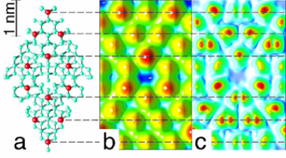
The Si(111) surface was simulated by a four layer silicon film, the bottom layer was passivated with hydrogen. The ionic positions were determined by fully relaxing the surface layers until the Hellman-Feynman forces on individual ions were less than 0.01eV/Å. The electronic groundstate was then calculated using ultrasoft pseudopotentials for the ionic cores with the Vienna ab-initio Simulation Program kresse93 ; kresse96 . Due to the size of the system, which comprises 249 ions in the unit cell, the calculation was limited to only one k-point, the point. The energy cutoff for the plane-wave expansion was set to 250 eV. The atomic arrangement in the final iteration and the (77) unit cell is shown in Fig. 1(a). After the electronic groundstate structure had been calculated the Kohn-Sham states in the energy interval eV were extracted. Testing the resolution of the ensuing images based on the electronic surface structure alone we found that the detailed features are quite sensitive to the cutoff in the two dimensional Fourier expansion of the single electron states. To obtain high resolution images it was necessary to expand every state with close to 500 reciprocal lattice vectors. The density of electron charge within the interval in a horizontal plane above the surface is shown in Fig. 1(b). The contributions to the charge density at -2 eV are shown in (c). It can be seen that the differential contributions show a double feature at the position of the adatoms, which is missing in the density contour over the whole bias interval. This indicates that the double features are due to electron states with an energy close to -2 eV relative to the Fermi level. An integration over the whole bias range sums up a large number of individual states, the double feature, which we attribute to single electron states, is then no longer observable.
The tip model in our simulations is a (22) Si(001) surface with a single silicon atom, as suggested by an analysis of high resolution AFM experiments giessibl00 . The tip was simulated by an eight layer film with a hydrogen passivated bottom layer. Since the tip system is somewhat smaller we increased the number of k-points of the tip system to nine k-points near the center of the tip Brillouin zone, including the point. The single silicon atom at the tip apex leads to two dangling bonds protruding from the tip apex. We simulated two STM tips, obtained by rotating the atoms of the original cell by 90 degrees while keeping the lattice vectors constant. To obtain the current maps and the locally resolved spectra of the surface we employed a newly developed method, described in hofer05a ; palotas05 . The scattering method, calculated to first order in the interface Green’s function accounts for the bias dependency with the help of an additional term, which depends on the bias potential and the exponential decay of surface and tip states , according to palotas05 :
| (1) | |||||
Here, is the Fermi distribution function, is the chemical potential of the surface (tip), the eigenvalue of surface (tip) states, and the Bardeen matrix element. The difference to the standard Bardeen method, the second term in the quadratic expression, arises from the shift of eigenstates due to the applied bias voltage. It accounts for the bias dependency in the tunnelling junction. High resolution spectra for the bias range V were directly calculated by a map of differential changes as the bias voltage is ramped up. The method, described in hofer05a is more efficient than numerically differentiating the map, it also allows to separate contributions due to the bandstructure of the STM tip.
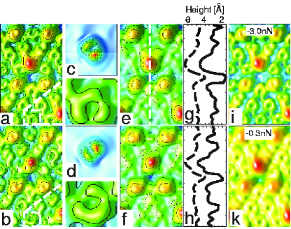
The experiments were conducted with a combined scanning tunneling/atomic force microscope at room temperature in an ultrahigh vacuum at mbar. The Si(111) sample (p-doped Si(111) wafer, resistivity 9.0 cm, MacTecK, Jülich, Germany) was prepared with a standard technique involving heating to 1280 ∘C for about 30 s. In order to facilitate comparison between theory and experiment, simultaneous force and current measurements are performed in the constant-height mode, where the tip scans in a plane parallel to the surface. Measuring the tip-sample forces directly is impractical because of experimental noise and strong background forces Giessibl:2003 . Therefore, we resort to frequency modulation force microscopy albrecht91 where the frequency shift of an oscillating cantilever is measured. We used a qPlus cantileverGiessibl:2000b in this study with a spring constant of N/m, an eigenfrequency of Hz and an oscillation amplitude of Å. While the tip of the force sensor consisted of an etched tungsten tip, we found that the active tip cluster consists of Si picked up from the surface during the tip preparation process that involves controlled collisions with the Si sample accompanied by voltage pulses. After this process, we frequently find craters on the Si surface where the missing sample material is not found anywhere close on the surface. Scanning electron microscopy images of these “tungsten”tips reveal sharp-edged clusters with a size similar to the observed craters on the surface ( nm). Because the tip oscillates, the experimental observable is an average tunneling current and a frequency shift . is given by the peak current divided by where is the decay rate of the tunneling current (Eq. 43 in Giessibl:2003 ). With Å-1 and as given above, we find a peak current of 10.8 times the average values given in the captions of Fig. 3. The frequency shift is given by where the range of the tip-sample force is given by hofer03a . The typical frequency shift in this experiment is -5 Hz, thus the estimated tip-sample force at closest distance is -5 nN. The results of topographic simulations at a bias voltage of -2V are shown in Fig. 2.
Simulations were performed with the tip unit cell of the extended Si(001) tip system aligned to the horizontal and vertical axes of the surface unit cell. For high current values of 0.5nA the topographic images show a double feature: two protrusions with a depression in vertical alignment for all adatoms of the surface, with the exception of one corner atom (Fig. 2(a)). The stability of the numerical results was analyzed by performing the simulations with 100, 200, or 488 lattice vectors. The results given are obtained with the expansion of highest resolution, but even in this case the double feature at one corner atom, which is clearly visible in high-resolution spectrum simulations (see further down), could not be resolved. In all other cases, however, the constant current contour reveals double features (Fig. 2(a) and (b)). The details of the features depend on the orientation of the tip, as a comparison between Fig. 2(a) and (b) reveals. The detail shows the shape of one protrusion, which is rotated if the tip rotates by ninety degrees. It is interesting to note that detail (d) is actually not only rotated, but also reflected compared to detail (c). The additional mirror plane reflects the reflected vertical orientation of the STM tip. For comparison, we also show constant force contours of the surface for 3.0nN and 0.3nN (Fig. reffig2 (i) and (k)), and one of the tip models. The simulations establish that the origin of the double feature is the convolution of surface states at the Si(111) surfaces and states at the mono-atomic Si(001) tip. By contrast, a simulated scan of the same surface with a tungsten tip does not show any double features even at very close distances. This is quite understandable, if one considers the spatial distribution of dangling bonds on the front atom of the silicon tip, which is much more focussed than that of the electron states at the apex of a tungsten tip. In addition, the local resolution is diminished by a large number of nearly equivalent tip states, which can be used as a drain for tunnelling electrons.
The occurrence of double features in the constant current contours is distance dependent. Figs. 2(e) and (f) show constant current contours of 20 pA. At this current, which is roughly in the range of most STM experiments, the double features at the positions of silicon adatoms have nearly vanished. The median distance at this current value, shown in the linescans (g) and (h), is still only about 4 Å, which is a range that is too close for conventional STM. It seems that even with a silicon tip apex in (001) orientation, the features are difficult to observe in conventional STM experiments. To sum up the argument, we may say that even though the double features pertain to the electronic structure of the silicon surface, they are only visible in dynamic STM herz03 or dynamic AFM with a very peculiar choice for the tip. The reason, that dynamic STM/AFM can scan at distances of less than 3 Å, i.e. in a range, where the tip of conventional STM is broken, is the near absence of shear forces on the tip. An equivalent situation in STM experiments would be an approach and retraction cycle, and in this case it has been shown that the STM tip can approach to the point of contact without breaking cross98 ; limot05 .
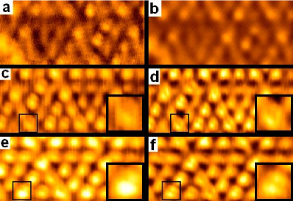
In Fig. 3 we show simultaneously acquired images of the current averaged over one oscillation (Fig. 3(a), (c), and (e)) and the frequency shift (Fig. 3(b), (d), and (f)) in a combined AFM/STM experiment. Up to a current of 0.5nA, which is well above the level in STM scans without an oscillating cantilever, the current contours do not show a double feature in the images, even though the protrusions correspond to the protrusions in the frequency shift image.
This indicates, as already pointed out in a previous paper hembacher04 , that current and interaction energy are indeed related. But considering that the double feature is present in the corner atoms at very close distances (Fig. 3(f)), it also reveals that the relation is not strictly linear at very low distances. The frequency shift in this case seems more sensitive to the details of the electronic structure than the current contour. In addition, the different orientation of the double features points to a rotation of the tip compared to the models used in the simulations.
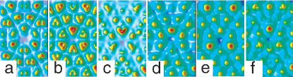
In principle, the choice of the AFM tip model should also play a role in AFM simulations, if the resulting forces are simulated by moving a tip cluster above the silicon surface and calculating the ensuing interactions of the coupled system by density functional theory sim_2003 . However, there is one qualification: interactions and forces depend on the transition of electrons from one side of the coupled system to the other hofer03b . If the energy difference between individual electron states of the decoupled subsystems is too large, the transmission probability will be reduced and the interaction energy will not be strongly affected. This means that the states of surface and tip, leading to the double features, must possess similar energies. The conjecture was checked by spectroscopy simulations with high local resolution, using the same silicon tip. Selected results of the obtained maps are shown in Fig. 4. It can be seen that differential contributions show the double feature primarily in the bias range below -1.5 V (Fig. 4(a) and (b)). In the positive bias regime the adatoms are uniquely imaged as single protrusions (Fig. 4(d), (e), and (f)). Comparing with experimental conditions in most STM images of the Si(111) surfaces it seems that this characteristic of images is one of the reasons for choosing primarily positive bias voltages corresponding to electrons tunnelling from filled tip states into empty surface states. Around the Fermi level the conductance and also the obtained current values are very low. However, we also note double features in the conductance contours in this range. This seems to explain to some extent the results of recent simulations. As AFM simulations are performed with zero bias, the transitions responsible for chemical interactions hofer03a involve primarily states in this range, which could lead to double features, even though their corrugation will be significantly smaller than in the negative bias regime. We may conclude from these results that the experimental data, obtained by AFM giessibl00 , which were taken at a sample bias of -1.5 V, utilized one range, where the double features appear. By contrast, the simulations, performed at zero bias, correspond to a different range. The whole picture only emerges, when the contributions to the tunnelling currents at varying bias are analyzed in detailed images with high local resolution. One may extend the analysis by a conjecture concerning AFM scans on insulating surfaces. Since the overlap between surface and tip states plays an essential role in the obtained interaction energy, tuning the bias voltage in AFM scans to a suitable range may substantially improve the resolution also in these cases. Arai and Tomitori have recently found, that a strong bias dependence also occurs in AFM imaging at greater tip-sample distances arai04 .
In summary we have shown that the sub-atomic features arise from a convolution of the electronic structure of the silicon surface and a silicon tip that is highly bias dependent. These features can be observed by both STM and AFM, if the tip-sample distance is sufficiently small. Stability considerations require the use of oscillating tips to reduce lateral forces when scanning very close to the sample. The occurrence of double peaks for single Si atom images is also limited to two narrow bias ranges: below about -1.5 V, and near the Fermi level in the positive bias regime.
LAZ is funded by EPSRC grant GR/T18592/01. WAH is supported by the Royal Society through a University Research Fellowship. The experimental work has been funded by BMBF grant EKM13N6918. We also acknowledge help from O. Paz and J. Soler with the setup of the Si(111) (77) unit cell.
References
- (1) G. Binnig et al., Phys. Rev. Lett. 56, 930 (1986)
- (2) F. J. Giessibl et al., Science 289, 422 (2000)
- (3) M. Huang et al., Phys. Rev. Lett. 90, 256101 (2003)
- (4) H. Hug et al., Science 291, 2509a (2001)
- (5) M. A. Lantz et. al. Science 291, 2580 (2001)
- (6) S. Hembacher et al., Science 305, 380 (2004)
- (7) T. Eguchi et al., Phys. Rev. Lett. 93, 266102 (2004)
- (8) W. A. Hofer et al., Rev. Mod. Phys. 75, 1287 (2003)
- (9) G. Kresse et al., Phys. Rev. B 47, 558 (1993)
- (10) G. Kresse et al., Phys. Rev. B 54, 11169 (1996)
- (11) O. Paz et al., Phys. Rev. Lett. 94, 056103 (2005)
- (12) W. A. Hofer et al., Phys. Rev. B 71, 085401 (2005)
- (13) K. Palotas et al., J. Phys: Condens. Mat. 17, 2705 (2005)
- (14) W. A. Hofer et al., Phys. Rev. Lett. 91, 036803 (2003)
- (15) G. Cross et al., Phys. Rev. Lett. 80, 4685 (1998)
- (16) M. Herz et al., Phys. Rev. B 68, 045301 (2005)
- (17) L. Limot et al., Phys. Rev. Lett. 94, (2005)
- (18) F. J. Giessibl, Appl. Phys. Lett. 76, 1470 (2000)
- (19) S. Hembacher et al., Phys. Rev. Lett. 94, 056101 (2004)
- (20) F. J. Giessibl, Rev. Mod. Phys. 75, 949 (2003)
- (21) T.R. Albrecht et al., J. Appl. Phys. 69, 668 (1991).
- (22) T. Arai et al., Phys. Rev. Lett. 93, 256101 (2004)